Article

Argon and Other Defects in Amorphous SiO2 Coatings for Gravitational-Wave Detectors

by
Annalisa Paolone
1,2,*,
Ernesto Placidi
2,3,
Elena Stellino
4,
Maria Grazia Betti
2,3,
Ettore Majorana
2,3,
Carlo Mariani
2,3,
Alessandro Nucara
3,
Oriele Palumbo
1,
Paolo Postorino
3,
Marco Sbroscia
3,
Francesco Trequattrini
3,
Massimo Granata
5,
David Hofman
5,
Christophe Michel
5,
Laurent Pinard
5,
Anaël Lemaitre
6,
Nikita Shcheblanov
6,
Gianpietro Cagnoli
7 and
Fulvio Ricci
2,3
1
Consiglio Nazionale delle Ricerche, Istituto dei Sistemi Complessi, Piazzale A. Moro 5, I-00185 Roma, Italy
2
Istituto Nazionale di Fisica Nucleare, Piazzale A. Moro 5, I-00185 Roma, Italy
3
Dipartimento di Fisica, Sapienza Università di Roma, Piazzale A. Moro 5, I-00185 Roma, Italy
4
Dipartimento di Fisica e Geologia, Università di Perugia, Via Pascoli, I-06123 Perugia, Italy
5
Laboratoire des Matériaux Avancés—IP2I, CNRS, Université de Lyon, Université Claude Bernard Lyon 1, F-69622 Villeurbanne, France
6
Laboratoire Navier, Ecole des Ponts, Université Gustave Eiffel, CNRS, F-77420 Marne-la-Vallée, France
7
Laboratoire de Physique, ENS de Lyon, Université Claude Bernard Lyon 1, CNRS, F-69342 Lyon, France
*
Author to whom correspondence should be addressed.
Coatings 2022, 12(7), 1001; https://doi.org/10.3390/coatings12071001
Submission received: 8 June 2022 / Revised: 8 July 2022 / Accepted: 11 July 2022 / Published: 15 July 2022

Abstract

:
Amorphous SiO2 thin films are one of the two components of the highly reflective mirror coatings of gravitational-wave detectors. For this study, layers of amorphous SiO2 on crystalline Si substrates were produced by ion-beam sputtering (IBS), using accelerated neutralized argon ions as sputtering particles, as is the case for the actual mirror coatings of gravitational-wave detectors. The aim of this study is to investigate the possible presence of various defects in the materials in order to improve the coating quality. We provide evidence that, due to the synthesis method, about 0.2 wt.% of Ar is present in the coatings, and it can be released by means of thermal treatments, starting around 400 °C. The time and temperature to obtain the total release of Ar increases with the coating thickness; for a thickness of 100 nm, all argon is released below 600 °C, while an isotherm of one hour at 900 °C is necessary for a coating 5 μm thick. Besides the Ar atoms left from the synthesis, other defects, such as Si clusters and silicon dangling bonds, are present in the coatings. The concentration of both of them is strongly reduced by thermal treatments either in vacuum or in air. The overall thickness of the coating is slightly increased after thermal treatments, as witnessed by the change of the period of interference fringes.

1. Introduction

One of the most relevant and unavoidable limitations for precision experiments in the field of interferometric gravitational-wave detectors [1], optomechanical resonators [2], and frequency standards [3] is the Brownian thermal noise occurring in highly reflective coatings [4,5]. Its power spectral density, S, when measured by means of a laser beam, obeys the following relation [6]:
S k B T 2 π f d w 2 φ
where kB is the Boltzmann constant, T is the temperature, f is the frequency, d is the coating thickness, w is the laser beam radius where the intensity drops by 1/e, and φ is the coating loss angle. This last quantity indicates how much mechanical energy is dissipated in the coating and it is a function of both frequency and temperature, φφ(f, T). In order to reduce the contribution of the coating thermal noise, there are some possible strategies: an increase of the beam radius, a reduction of the temperature, or the choice of a coating with a minimal value of the product of d and φ in Equation (1).
High-reflective (HR) coatings are usually Bragg reflectors composed by alternating layers of materials with high (nH) and low (nL) refractive indices. A key parameter is the refractive index contrast, C = nH/nL, as the coating thickness, d, is a monotonically decreasing function of C. Therefore, by increasing C, one can have the same reflectivity by using thinner HR coatings with a consequent reduction of the coating thermal noise.
The presently used high-reflective coatings of the mirrors of the Advanced LIGO [7], Advanced Virgo [8], and KAGRA [9] gravitational-wave detectors are optimized stacks [10] of amorphous tantalum pentoxide (Ta2O5, also known as tantala, with a high refractive index nH ≈ 2.05) and amorphous silicon dioxide (SiO2, silica, with a low refractive index nL ≈ 1.44) produced by the Laboratoire des Matériaux Avancés (LMA) by means of ion-beam sputtering (IBS) [11,12,13]. To reduce both the optical absorption and the coating loss angle of Advanced LIGO and Advanced Virgo mirrors, LMA also added a significant amount of titanium dioxide (TiO2, titania) to the tantala high-index layers [13,14].
Despite this optimization process and the very good optical and mechanical properties of the presently used coatings [12,13,15], their thermal noise still remains one of the main factors limiting the sensitivity of gravitational-wave detectors. Therefore, in the last twenty years, a deeper investigation of materials for coatings has been performed with the aim of reducing both the mechanical and the optical losses [16]. One strategy is using alternative coating materials, especially for low-temperature applications, such as the cryogenic gravitational-wave detectors, e.g., KAGRA, Einstein Telescope [17,18], and Cosmic Explorer [19]. On the other hand, also an additional optimization of the presently used materials is explored, mainly concerning post-deposition annealing processes, which are known to decrease the coating mechanical losses. Indeed, there is clear evidence that the mechanical losses of the coating can be reduced by a thermal treatment for 10 h in air [13]. After this procedure, the tantala thin films reach the same value of dissipation independently of the synthesis method [13]. Longer thermal treatments do not further decrease the mechanical losses [20].
In this framework, in the last few years, more attention has been devoted to the microscopic properties of the materials composing the high-reflective coatings and their changes with thermal treatments. For example, Extended X-ray Absorption Fine Structure (EXAFS) [21] and Raman [20] measurements evidenced that, on a scale of 50 nm, the amorphous structure of Ta2O5 is preserved after heating at 300 and 600 °C in air. However, Fluctuation Electron Microscopy (FEM) measurements on IBS amorphous tantala coatings showed an ordering of the medium range structure on the length of 2 nm after a thermal treatment at 600 °C [22]. Changes of the intermediate range structure were also found in TiO2-Ta2O5 amorphous coatings [23]. More recently, the presence of argon in Ta2O5 due to the synthesis by IBS was reported [24]. Ar can be released by heating above 300 °C [24]. It was reported that the density of Ta2O5 decreases as the annealing temperature increases [24]. However, Ar can be trapped in voids of the amorphous structure; at high temperatures, the dimensions of these voids seem to increase, and the surface of the coating becomes damaged [20,25,26]. In particular, for TiO2-doped Ta2O5 with a Ti cation ratio of 0.27 after annealing, one obtains a homogeneous mixture, namely TiTa18O47, that displays the lowest mechanical loss [13,14,25]; at different cation concentrations, it seems that no homogeneous solution forms, and the sample is still constituted by the two initial phases, TiO2 and Ta2O5. Upon heating, the density of the material giving rise to TiTa18O47 decreases, and Transmission Electron Microscopy measurements evidenced the presence of closed voids, which become filled with Ar, having a typical diameter of 1–2 nm and a surface density of about 0.02 voids/nm2 [25]. Cummings et al. indicated that the argon bubbles start to form with thermal treatments at 400 °C and tend to merge after annealing at 600 °C [26]. The presence of nanobubbles filled with argon and oxygen was found also in other amorphous oxide thin films, such as hafnia-based (HfO2) [27] and niobia-based (Nb2O5) coatings [28].
In view of the increasing interest for the presence of argon in the layers of the HR coatings of gravitational-wave detectors, we investigated amorphous silica grown by IBS at LMA in order to detect the possible presence of argon; its release as a function of thickness, temperature, and atmosphere; and the occurrence of possible other defects in this material.

2. Materials and Methods

The amorphous SiO2 thin films studied in this work were synthesized at LMA by means of IBS in a commercial SPECTOR (Veeco, Plain View, New York, NY, USA) coating system, using accelerated neutralized argon ions as sputtering particles. All coatings were deposited on substrates made of crystalline Si. The base pressure of the vacuum chamber was in the 10−6 to 10−5 mbar range before the deposition. Argon and oxygen were fed into the ion-beam source, while oxygen was fed into the vacuum chamber, reaching a total residual working pressure of the order of 10−4 mbar, with a ratio of partial pressures Ar/O2 equal to ~0.8. The current and energy of the Ar sputtering ions were of the order of 0.1 A and 1 keV, respectively, and the resulting growth rate was ~0.3 nm/s. The sputtered particles impinged on a substrate heated up to about 100 °C.
The refractive index and thickness of the thin films were measured by transmission spectrophotometry through samples grown on fused-silica witness samples. A Lambda 1050 spectrophotometer (Perkin Elmer, Waltham, MA, USA) was used, where spectra were acquired at normal incidence in the 400–1400 nm wavelength range. The refractive index and thickness were first evaluated by using the envelope method [29], and then these results were used as initial values in a numerical least-square regression analysis. In the model, the adjustable parameters were the film thickness and the (Bi, Ci) coefficients of the Sellmeier dispersion equation:
n 2 = 1 + i = 1 3 B i λ 2 λ 2 C i ,
where λ is the wavelength.
Mass spectrometry measurements, which were used to investigate the release of Ar from the samples, were performed by means of a Pfeiffer Vacuum QMS200 quadrupole (Pfeiffer Vacuum, Asslar, Germany) mass spectrometer connected through a vacuum line to the oven of a Setaram Setsys Evolution 1200 thermogravimetric system (KEP Technologies Group, Mougins—Sophia Antipolis, France), which was used to heat the samples with a predefined temperature rate (3 °C/min). A vacuum of the order of 10−5 mbar was maintained in the furnace in order to increase the sensitivity of the mass spectrometer. The samples were heated from room temperature up to 900 °C, with a temperature rate of 3 °C/min, and afterward they were allowed to stay in isotherm mode at this maximum temperature for one hour. A sample mass of about 4 g was heated in each experiment. Two different thicknesses of the SiO2 coating deposited on crystalline Si were used (100 nm and 5 μm).
The X-ray photoelectron spectroscopy (XPS) experiments were carried out in ultrahigh vacuum (UHV), with a base pressure in the low 10−10 mbar range. Part of measurements were performed with a non-monochromatized X-ray photon source (PSP Vacuum Technology Ltd., Macclesfield, UK) (PSP TA10 Mg Kα, hν = 1253.6 eV); photoelectrons were measured with a hemispherical VG Microtech Clam-2 electron analyzer (VG Microtech, London, UK) in constant pass energy mode set at 50 eV and with overall energy resolution better than 1 eV in the LOTUS laboratory of the Physics Department at Sapienza University. Measurements of the samples heated at 500 °C were performed with an Al Kα monochromatic (1486.6 eV) X-ray source (XR50 MF) and with a SPECS PHOIBOS 150 analyzer (SPECS Surface Nano Analysis GmbH, Berlin, Germany), working with a pass energy of 20 eV, in the SMART laboratory of the Physics Department at Sapienza University. The binding energy (BE) scale was calibrated on a freshly sputtered gold foil in electrical contact with the sample by setting the Au 4f7/2 core-level at 84.0 eV BE. Overall, XPS experiments were performed both on the “as-deposited” samples and on small parts of the same samples heated either in vacuum at 300–450 °C in situ or in air at 500 °C for 10 h (ex situ). Samples annealed in UHV were measured in the LOTUS laboratory, while all the others were measured in the SMART laboratory. Untreated samples were measured in both apparatuses. Coatings of 5 μm in thickness were measured in the SMART laboratory, employing a neutralizer with an e- current of 70 μA and a 5 V voltage.
Raman and photoluminescence (PL) measurements were performed at ambient conditions, using a Horiba spectrometer (HORIBA, Ltd., Kyoto, Japan) equipped with a 532 nm laser, a 100× objective (light spot of ~2 μm2), and a grating monochromator with 600 grooves/mm. Each spectrum was the average of 3 acquisitions, with an exposition time of 5 s for each of them.
Mid-infrared reflectivity measurements were performed at ambient conditions, using a commercial Bruker Interferometer (Bruker, Billerica, MA, USA) coupled with an infrared microscope (Bruker Hyperion 2000) and a gold mirror as reference. The size of the incident light spot was fixed at 200 μm. Spectra were collected with 4 cm−1 resolution, and each spectrum was the average of 256 scans for each point. A nitrogen-cooled mercury–cadmium–telluride (MCT) and a potassium bromide (KBr) crystal were used as the detector and beamsplitter, respectively.

3. Results and Discussion

The characterization of the amorphous SiO2 coatings is presented in the next sub-sections, divided according to the used experimental technique, in the following order: mass spectrometry (Section 3.1), XPS (Section 3.2), photoluminescence (Section 3.3), and infrared spectroscopy (Section 3.4).

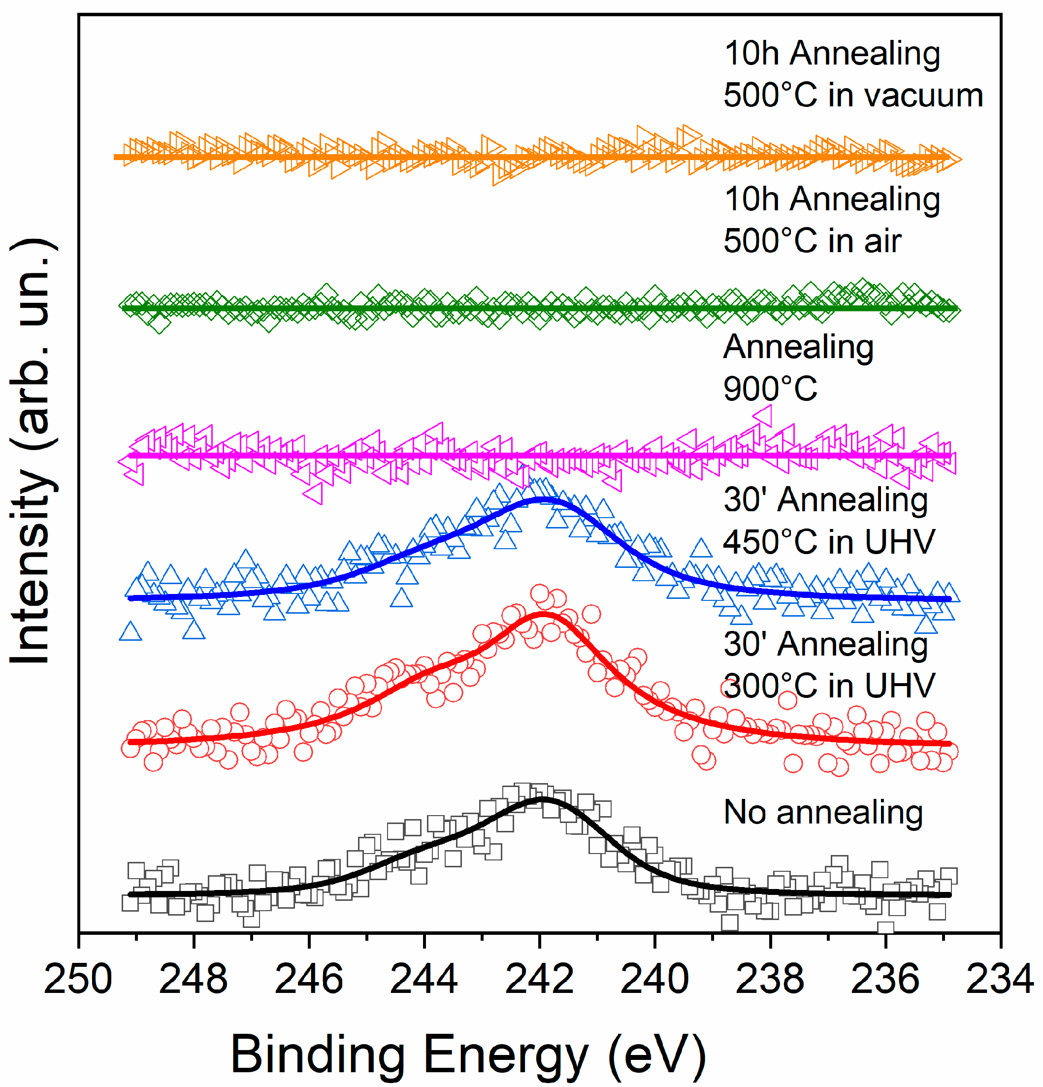
3.1. Effusion of Argon by Mass Spectrometry

Figure 1 reports the argon signal measured by the mass spectrometer for two SiO2 samples with a thickness of the coating of 100 nm and 5 μm.
The 100 nm–thick sample displays a peak in the effusion of argon starting around 400 °C, with a maximum at ≈570 °C; the subsequent increase of the Ar signal above 700 °C can be considered as a background, due to the unavoidable increase of the pressure in the oven at high temperatures. Indeed, during the isothermal annealing at 900 °C, the Ar signal of the 100 nm–thick sample remains constant, as well as the pressure inside the furnace. In the case of the 5 μm–thick sample, one can observe a much higher increase in the Ar signal above ~400 °C, up to 900 °C. In the subsequent isotherm at 900 °C, the Ar signal decreases as a function of time, with a trend to reach the background level. Therefore, in both samples, a release of argon above ~400 °C is visible.
The dependence of the effusion of argon from the thickness of the sample, both in intensity and as a function of temperature, strongly suggests that Ar is present in the whole thickness of the SiO2 coating, and it slowly diffuses toward the surface exposed to vacuum. If argon was present only on the surface, the release of Ar should not be dependent on the sample thickness. Around 400 °C, this process starts to take place, but it requires longer time to fully develop for thicker samples.
The temperature at which the argon release starts in SiO2 is much higher than that measured for Ta2O5, where argon discharge starts to be observable around 200 °C in a sample that is 953 nm thick, and the whole Ar release is completed around 500 °C for the same thickness [24]. This fact could be related to a lower trapping energy of Ar in Ta2O5 and/or to a lower diffusion coefficient in SiO2. To the best of our knowledge, no measure of the diffusion coefficient of argon in Ta2O5 is available. On the contrary, the diffusion coefficients of Ar and other gases in SiO2 glass were investigated a long time ago both around ambient pressure [30] and for pressures higher than 200 bar [31]. Temperatures between 400 and 900 °C were also considered [30,31]. The diffusion coefficient of Ar in SiO2 glass was reported to follow an Arrhenius law, D = D0 exp(−E/RT), with D0 (the maximal diffusion coefficient) of the order of 3 × 10⁻⁶ cm2/s [31] or 1 × 10⁻⁴ cm2/s [30]. The activation energy, E, was reported to be 22 [31] or 28 kcal/mol [30]. Keeping in mind the values of D0 and E reported in the literature [30,31], one would expect a diffusion coefficient, D, of the order of 10−13 and 10−10 cm2/s at 400 and 900 °C, respectively. In materials with easy diffusion of impurity atoms in solids, such as hydrogen in palladium, the temperature independent maximal diffusion coefficient, D0, is of the order of 2 × 10⁻³ cm2/s, and the activation energy is of the order of only 5 kcal/mol [32]. These figures provide a diffusion coefficient of the order of 5 × 10⁻⁵ cm2/s at 400 °C. The values reported for the diffusion of argon in SiO2 glass indicate that the process can occur with relatively slow kinetics for the temperatures considered in this study.
It must be noted that the difference in the Ar discharge properties of the Ta2O5 (fast discharge at lower temperatures) and SiO2 (slower discharge at higher temperatures) materials is relevant, as the highly reflective coatings of the mirrors of the gravitational-wave interferometers consist in a stack of a large number of Ta2O5 and SiO2 layers [14]. Work is ongoing to investigate the argon release from stacked layers

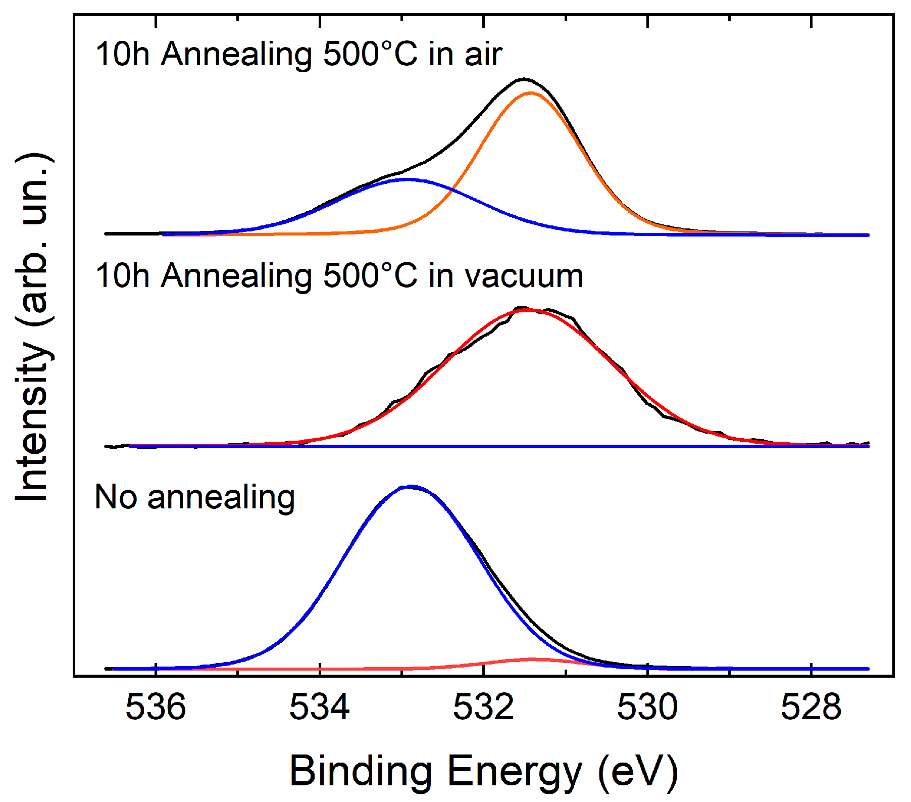
3.2. Effusion of Argon by XPS

To detect the possible presence of argon and to monitor its release as a function of temperature in vacuum and in air, as well as to control the occurrence of possible other defects in this material, we performed an XPS study of the amorphous SiO2 thin films. The XPS survey spectra (see Supplementary Materials Figure S1) presents the Si 2p and O 1s core levels of the SiO2 thin films, pointing out the absence of contaminations, apart from a small signal of carbon, as is common to many specimens.
Focusing on the Ar contribution (Figure 2), the Ar 2p components are visible in a broad peak at a binding energy of about 242 eV, with an estimated Ar weight with respect to the other elements around 0.2%; this value is slightly reduced (5%–10%) in the 100 nm–thick samples by thermal treatments in vacuum at 450 °C. This result is in agreement with the mass spectrometry measurements indicating that Ar release starts around 400 °C. The sample heated in vacuum, at 900 °C, for 1 h, for mass spectrometry measurements (5 μm thickness), after cooling back to room temperature, does not show the Ar 2p peak (Figure 2); therefore, after the treatment, there is no Ar on the first sample surface, thus suggesting that all the Ar from the film has been out-gassed.
More interestingly, in view of their application, we investigated by XPS some amorphous SiO2 films that were 100 nm thick and subjected to the same thermal treatment (10 h at 500 °C in air [14]) used for the coatings of the gravitational-wave detectors’ mirrors. This thermal treatment was performed in a GSL-1100X furnace of MTI corporation. The corresponding XPS spectra in Figure 2 show no feature corresponding to the Ar 2p peak, confirming that a 10 h annealing (either in air or in vacuum) is enough to remove all the Argon from the film, at least within the sensibility of the technique.
In Figure 3, we show the effects of annealing on the O 1s core level of SiO2 thin films. While the O1s peak of the untreated sample exhibits an almost pure higher energy component corresponding to the oxygen bound to Si in SiO2 at about 533 eV binding energy (blue lines in Figure 3), the samples thermally treated clearly show oxygen depletion effects with the occurrence of an O1s component at lower binding energy located at around 531.5 eV (orange and red lines in Figure 3). The oxygen depletion on the surface is complete in vacuum, while the annealing in air leaves the higher energy component, although remarkably reduced in intensity. The occurrence of a Si-O-H component (at 531.5 eV) during the annealing is likely since hydrogen is the main component of the residual gas of an UHV systems. Indeed, the literature investigations reported the formation of Si-O-H bonds in SiO2 even when silicon oxide was heated in a dry oxygen atmosphere, due to the residues of hydrogen and water that are inevitably present in the gas [33].

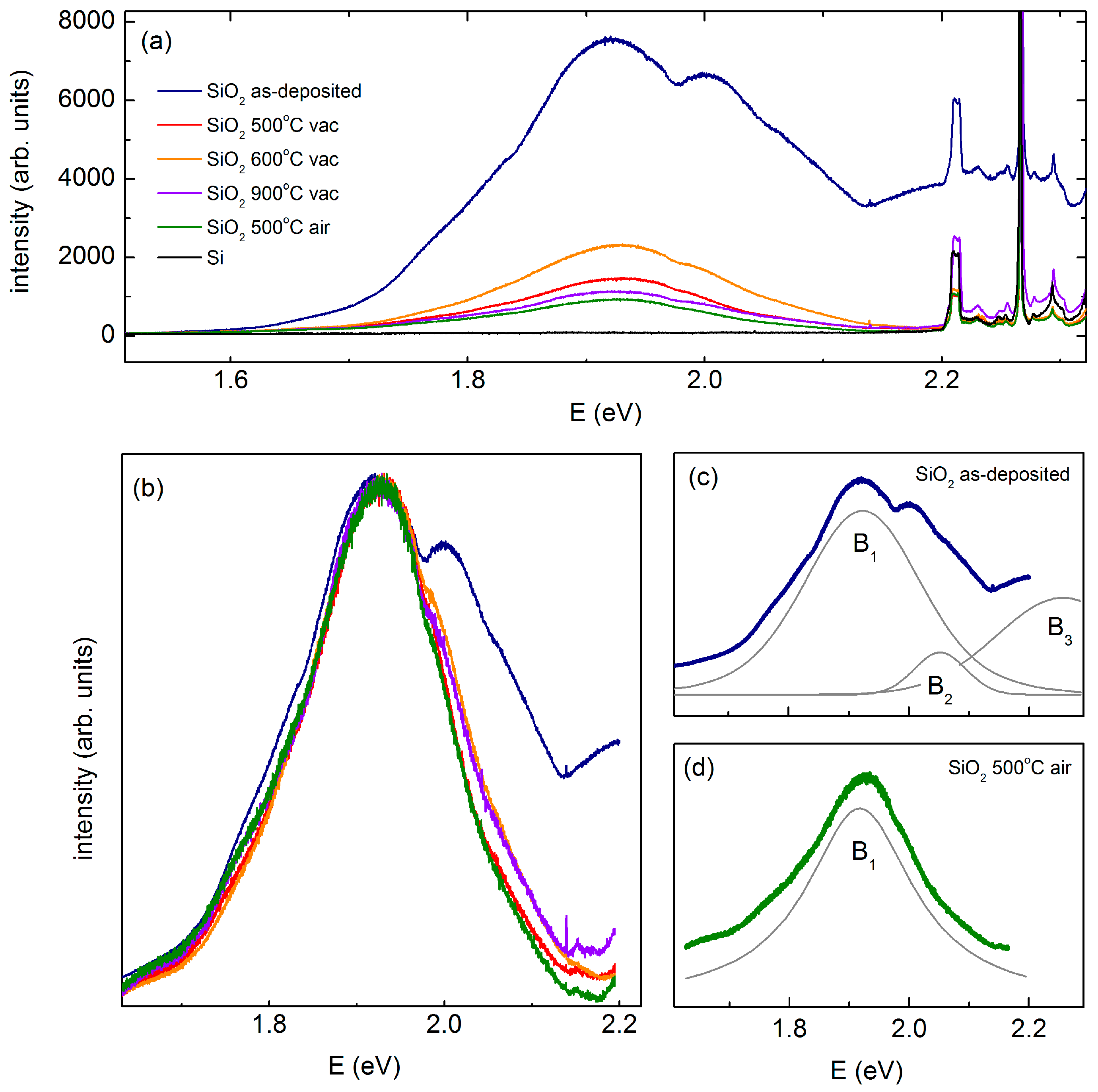
3.3. Defects in the Coating Layer by Photoluminescence

To gain information about the possible presence of defects in SiO2 layers, photoluminescence (PL) spectra were measured in the range 1.5–2.3 eV on 5 μm–thick samples that were subjected to different thermal treatments, as reported in Figure 4a. Each spectrum results from the average of five spectra collected from different points of the sample.
All the measured samples exhibit a Raman spectrum in the range 2.2–2.3 eV (i.e., 150–1100 cm−1 in Raman shift) which can be exclusively attributed to contributions from the Si substrate and does not appreciably vary depending on the thermal treatment (see Supplementary Materials Figure S2). Small differences in the intensity of the peaks could reasonably be ascribed to a different orientation of the samples or a slightly different focus of the laser spot during the measurements. Conversely, in the PL spectrum, the signal from the bare Si substrate is negligible below 2.2 eV (see Figure 4a), and, therefore, the bands observed in this energy range for the coated samples can be attributed to amorphous SiO2 films. It is worth noticing that, in this case, since the intensity of the signal scales with the film thickness (see Supplementary Materials Figure S3), we do not expect the Si/SiO2 interface to significantly contribute to the measured photoluminescence spectra.
The PL spectrum of the as-deposited sample is characterized by three different broad bands: B1~1.9, B2~2.0, and B3~2.3 eV (see Figure 4c). B3 originates from Si clusters embedded in the amorphous film, as reported in Reference [34]. B1 and B2, on the other hand, are due to Si dangling bonds [35,36]. In particular, according to Reference [36], the presence of two distinct sub-bands in the energy range 1.9–2.0 eV suggests a concentration of dandling bonds on the sample surface, whereas a unique peak would have implied a preferential location in the bulk.
After the thermal treatment in vacuum at 500, 600, and 900 °C, the intensity of the PL signal significantly decreases, and the overall profile of the spectrum is modified: the splitting between B1 and B2 reduces, and B3 almost vanishes, giving rise to a nearly single-peaked curve (see Figure 4b). These changes can be attributed to an annealing-induced reduction of Si dangling bonds that occurs preferentially on the sample surface.
Thermal treatment in air at 500 °C for 10 h induces similar changes in the PL spectrum (Figure 4d). The decrease in the B1 intensity and the suppression of the B2 band suggest a significant reduction of the Si-dandling bonds, particularly on the sample surface. Similarly, the absence of the band B3 indicates the extinction of the Si cluster embedded in the film.
It can be noted that, in Figure 4a, the intensity of the bands measured for the sample heated in vacuum at 600 °C is higher than that of the specimen heated at 500 °C; this might be due to the fact that, for the former sample, the thermal treatment lasted a few minutes, while for the latter one, it lasted 10 h. However, the treatment in air at 500 °C for 10 h is the one that gives the lowest intensity of the PL bands due to the Si dangling bonds. The results of the photoluminescence measurements are not in contrast with XPS spectra on O1s, and no evidence about the variation of Si-Si bonds was detected.

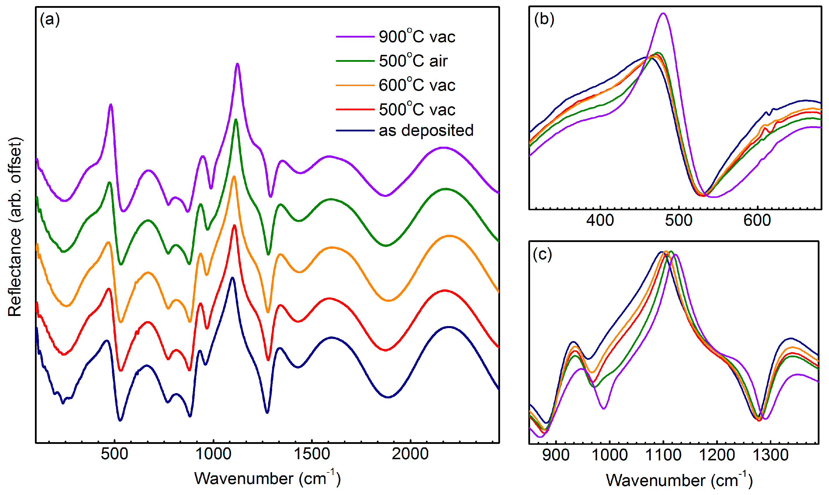
3.4. Infrared Spectroscopy

Reflectance spectra in the far- and mid-infrared range (100–6000 cm−1) are reported in Figure 5. The low-frequency region (100–1300 cm−1) is dominated by the phonon contributions, while, at higher frequencies, we can see intense oscillating fringes, due to infrared radiation interference between the film surfaces. As the annealing temperature (T) increases, the phonon peaks at ~500 and at ~1100 cm−1 shift toward higher frequencies, and their profiles progressively become more resolved (see Figure 5b,c).
The behavior of the fringe period (Supplementary Materials Figure S4) is slightly different from that measured in Ta2O5. In the latter case, thermal treatment at 500 °C in vacuum caused an increase in the Ta2O5 thickness of 1%, while a 2% increase was registered for thermal treatments at 500 °C in air [24]. In the present case, on the other hand, for an annealing temperature of 500 °C, one obtains a decrease in the fringe period (and, therefore, an increase in the sample thickness) of ~1% either in air or in vacuum. A more significant decrease of the fringe period, around 2%, is instead obtained when the sample is annealed at 900 °C in vacuum. For more details, see Supplementary Materials Figure S4.
To obtain quantitative information about the phonon contributions to the reflectance spectra, the interference fringes were removed by applying a standard Fourier-transform procedure, and the resulting data were fitted by a double-layer Drude–Lorentz model to account for both the SiO2 film and the Si substrate (the refractive index of the Si substrate was taken from the literature [37]). Finally, the real part of the optical conductivity was calculated by using the parameters obtained from the previous fit (see Figure 6a), and the phonon peaks in the conductivity spectrum were assigned to specific vibrational modes by a comparison with the literature [38].
The conductivity spectra, as reported in Figure 6, confirm a significant modification of the SiO2 vibrational modes after the annealing treatment, especially in the high-frequency side of the spectrum (~1000 cm−1). Indeed, a shift of the frequency of the reflectance band located around 1100 cm−1 was also reported by Hirose et al. [39]. The authors mainly investigated the evolution of the infrared spectrum of films of SiO2 deposited on crystalline SiO2 substrates after thermal treatments above 1000 °C for times up to ~1000 h [39]. Hirose noticed that the frequency of the peak is lower than that of bulk silica glass by 8 cm−1; it shifts toward higher wavenumbers as the thermal treatment temperature increases, reaching a maximum of 1124 cm−1 for T = 1000 °C; then it linearly decreases down to 1120.5 cm−1 for T = 1500 °C [39]. The shift of the position of this reflectance peak was attributed to the changes of the Si-O-Si angle induced by the thermal treatments [39] and presented as a clear indication of the relaxation of the amorphous SiO2 structure induced by thermal treatments. In the present work, most of the thermal treatments were performed at temperatures lower than the minimum temperatures used by Hirose (750 °C); however, a clear indication of structural relaxation is evident also in our coating samples. This is compatible with the outcomes of a previous study we carried out on similar coating samples [40]. It is interesting to notice that the peak measured for the sample heated in air at 500 °C is found at higher wavenumbers compared to that of the specimen heated at the same temperature in vacuum (see inset in Figure 6b). It must be noted also that a reduced content of oxygen in SiO2 can induce a red shift in the phonon frequency [41]. This fact may explain the higher vibrational frequency found in the sample heated in air at 500 °C. It must pointed out that this shift is very small, and, therefore, the possible reduction of oxygen in vacuum should also be very small.

4. Conclusions

An amorphous SiO2 coating deposited on crystalline silicon by means of IBS was investigated regarding the residual presence of argon due to the synthesis, its release at high temperatures, and the possible occurrence of other defects. An initial content of about 0.2 wt.% of Ar was left in the coating by the synthesis process. It starts to be released above ~400 °C in vacuum. Thinner samples complete the effusion of Ar at lower temperatures than thicker ones (≈600 °C for a thickness of 100 nm, and one hour at 900 °C for a thickness of 5 μm). A thermal treatment at 500 °C in air for 10 h, which usually is performed to decrease the mechanical loss of gravitational wave mirrors, is effective in removing Ar initially present in the samples. Si clusters, as well as silicon dangling bonds, are also present in the amorphous SiO2 coatings. The concentration of these defects strongly decreases after thermal treatments. Finally, a small increase of the film thickness appears after heating either in air or in vacuum.

Supplementary Materials

The following supporting information can be downloaded at https://www.mdpi.com/article/10.3390/coatings12071001/s1. Figure S1: XPS survey spectra acquired on SiO2 as a function of sample annealing temperature. Figure S2:Raman spectra of SiO2 films subjected to different annealing treatments. Figure S3: Comparison between the PL spectra of SiO2 films with different thicknesses: 100 nm (light blue) and 5 µm (dark blue). Figure S4: Interference fringes in the reflectance spectra of SiO2 films subjected to different annealing treatments. The offsets were shifted, and the phases of the fringes were adjusted in order to ease the comparison between the spectra. Colored arrows represent an estimate of the distance between two consecutive maxima.

Author Contributions

Conceptualization, A.P., G.C., and F.R.; methodology, A.P., G.C., and F.R.; validation, A.P., E.P., E.S., M.G.B., E.M., C.M. (Carlo Mariani), A.N., O.P., P.P., M.S., F.T., M.G., D.H., C.M. (Christophe Michel), L.P., A.L., N.S., G.C. and F.R.; formal analysis, A.P., E.P., E.S., A.N. and P.P.; investigation, A.P., E.P., E.S., M.G.B., E.M., C.M. (Carlo Mariani), A.N., O.P., P.P., M.S., F.T., M.G., D.H., C.M. (Christophe Michel), L.P., A.L., N.S., G.C. and F.R.; resources, M.G., D.H., C.M. (Christophe Michel), L.P., A.L. and N.S.; writing---original draft preparation, A.P., E.P. and M.G.; funding acquisition, A.P., M.G.B., C.M. (Carlo Mariani), E.P., E.M., F.R. and G.C. All authors have read and agreed to the published version of the manuscript.

Funding

This research was partially supported by the MIUR program “Dipartimento di Eccellenza” (CUP:B81I18001170001).

Institutional Review Board Statement

Not applicable.

Informed Consent Statement

Not applicable.

Data Availability Statement

Data are contained within the article or Supplementary Materials.

Acknowledgments

The present work was performed in the framework of the Virgo Coating Research and Development collaboration.

Conflicts of Interest

The authors declare no conflict of interest.

References

  1. Adhikari, R.X. Gravitational radiation detection with laser interferometry. Rev. Mod. Phys. 2014, 86, 121–151. [Google Scholar] [CrossRef]
  2. Aspelmeyer, M.; Kippenberg, T.J.; Marquardt, F. Cavity optomechanics. Rev. Mod. Phys. 2014, 86, 1391–1452. [Google Scholar] [CrossRef]
  3. Matei, D.G.; Legero, T.; Häfner, S.H.; Grebing, C.; Weyrich, R.; Zhang, W.; Sonderhouse, L.; Robinson, J.M.; Ye, J.; Riehle, F.; et al. 1.5 μm Lasers with Sub-10 mHz Linewidth. Phys. Rev. Lett. 2017, 118, 263202. [Google Scholar] [CrossRef] [PubMed] [Green Version]
  4. Saulson, P.R. Thermal noise in mechanical experiments. Phys. Rev. D 1990, 42, 2437–2445. [Google Scholar] [CrossRef] [PubMed]
  5. Levin, Y. Internal thermal noise in the LIGO test masses: A direct approach. Phys. Rev. D 1998, 57, 659–663. [Google Scholar] [CrossRef] [Green Version]
  6. Harry, G.M.; Gretarsson, A.M.; Saulson, P.R.; Kittelberger, S.E.; Penn, S.D.; Startin, W.J.; Rowan, S.; Fejer, M.M.; Crooks, D.R.M.; Cagnoli, G.; et al. Thermal noise in interferometric gravitational wave detectors due to dielectric optical coatings. Class. Quantum Grav. 2002, 19, 897–917. [Google Scholar] [CrossRef]
  7. Aasi, J.; Abbott, B.P.; Abbott, R.; Abbott, T.; Abernathy, R.M.; Ackley, K.; Adams, C.; Adams, T.; Addesso, P.; Adhikari, R.X.; et al. Advanced LIGO. Class. Quantum Grav. 2015, 32, 074001. [Google Scholar]
  8. Acernese, R.; Agathos, M.; Agatsuma, K.; Aisa, D.; Allemandou, L.; Allocca, A.; Amarni, J.; Astone, P.; Balestri, G.; Ballardin, G.; et al. Advanced Virgo: A second-generation interferometric gravitational wave detector. Class. Quantum Grav. 2015, 32, 024001. [Google Scholar] [CrossRef] [Green Version]
  9. Aso, Y.; Michimura, Y.; Somiya, K.; Ando, M.; Miyakawa, O.; Sekiguchi, T.; Tatsumi, D.; Yamamoto, H.; The KAGRA Collaboration. Interferometer design of the KAGRA gravitational wave detector. Phys. Rev. D 2013, 88, 043007. [Google Scholar] [CrossRef] [Green Version]
  10. Villar, A.E.; Black, E.D.; DeSalvo, R.; Libbrecht, K.G.; Michel, C.; Morgado, N.; Pinard, L.; Pinto, I.M.; Pierro, V.; Galdi, V.; et al. Measurement of thermal noise in multilayer coatings with optimized layer thickness. Phys. Rev. D 2010, 81, 122001. [Google Scholar] [CrossRef] [Green Version]
  11. Pinard, L.; Michel, C.; Sassolas, B.; Balzarini, L.; Degallaix, J.; Dolique, V.; Flaminio, R.; Forest, D.; Granata, M.; Lagrange, B.; et al. Mirrors used in the LIGO interferometers for first detection of gravitational waves. Appl. Opt. 2017, 56, C11–C15. [Google Scholar] [CrossRef] [PubMed] [Green Version]
  12. Degallaix, J.; Michel, C.; Sassolas, B.; Allocca, A.; Cagnoli, G.; Balzarini, L.; Dolique, V.; Flaminio, R.; Forest, D.; Granata, M.; et al. Large and extremely low loss: The unique challenges of gravitational wave mirrors. J. Opt. Soc. Am. A 2019, 36, C85–C94. [Google Scholar] [CrossRef] [PubMed]
  13. Granata, M.; Amato, A.; Balzarini, L.; Canepa, M.; Degallaix, J.; Forest, D.; Dolique, V.; Mereni, L.; Michel, C.; Pinard, L.; et al. Amorphous optical coatings of presentgravitational-waveinterferometers. Class. Quantum Grav. 2020, 37, 095004. [Google Scholar] [CrossRef] [Green Version]
  14. Harry, G.M.; Abernathy, M.R.; Becerra-Toledo, A.E.; Armandula, H.; Black, E.; Dooley, K.; Eichenfield, M.; Nwabugwu, C.; Villar, A.; Crooks, D.R.M.; et al. Titania-doped tantala/silica coatings for gravitational-wave detection. Class. Quantum Grav. 2007, 24, 405–415. [Google Scholar] [CrossRef]
  15. Amato, A.; Terreni, S.; Dolique, V.; Forest, D.; Gemme, G.; Granata, M.; Mereni, L.; Michel, C.; Pinard, L.; Sassolas, B.; et al. Optical properties of high-quality oxide coating materials used in gravitational-wave advanced detectors. J. Phys. Mater. 2019, 2, 035004. [Google Scholar] [CrossRef]
  16. Granata, M.; Amato, A.; Cagnoli, G.; Coulon, M.; Degallaix, J.; Forest, D.; Mereni, L.; Michel, C.; Pinard, L.; Sassolas, B.; et al. Progress in the measurement and reduction of thermal noise in optical coatings for gravitational-wave detectors. Appl. Opt. 2020, 59, A229–A235. [Google Scholar] [CrossRef]
  17. Hild, S.; Abernathy, M.; Acernese, F.; Amaro-Seoane, P.; Andersson, N.; Arun, K.; Barone, F.; Barr, B.; Barsuglia, M.; Beker, M.; et al. Sensitivity studies for third-generation gravitational wave observatories. Class. Quantum Grav. 2011, 28, 094013. [Google Scholar] [CrossRef]
  18. Abernathy, M.; Acernese, F.; Ajith, P.; Allen, B.; Amaro-Seoane, P.; Andersson, N.; Aoudia, S.; Astone, P.; Krishnan, B.; Barack, L.; et al. Einstein Telescopec onceptual Design Study, ET Technical Note ET-0106C-10. 2011. Available online: https://tds.ego-gw.it/ql/?c=7954 (accessed on 8 July 2022).
  19. Abbott, B.P.; Abbott, R.; Abbott, T.D.; Abernathy, M.R.; Ackley, K.; Adams, C.; Addesso, P.; Adhikari, R.X.; Adya, V.B.; Affeldt, C.; et al. The LIGO Scientific Collaboration. Exploring the Sensitivity of Next Generation Gravitational Wave Detectors. Class. Quantum Grav. 2017, 34, 044001. [Google Scholar] [CrossRef] [Green Version]
  20. Amato, A.; Cagnoli, G.; Canepa, M.; Coillet, E.; Degallaix, J.; Dolique, V.; Forest, D.; Granata, M.; Martinez, V.; Michel, C.; et al. High-reflection coatings for gravitational-wave detectors: State of the art and future developments. J. Phys. Conf. Ser. 2018, 957, 012006. [Google Scholar] [CrossRef] [Green Version]
  21. Bassiri, R.; Liou, F.; Abernathy, M.R.; Lin, A.C.; Kim, N.; Mehta, A.; Shyam, B.; Byer, R.L.; Gustafson, E.K.; Hart, M.; et al. Order within disorder: The atomic structure of ion-beam sputtered amorphous tantala (a-Ta2O5). APL Mater. 2015, 3, 036103. [Google Scholar] [CrossRef] [Green Version]
  22. Hart, M.J.; Bassiri, R.; Borisenko, K.B.; Véron, M.; Rauch, E.F.; Martin, I.W.; Rowan, S.; Fejer, M.M.; MacLaren, I. Medium range structural order in amorphous tantala spatially resolved with changes to atomic structure by thermal annealing. J. Non-Cryst. Solids 2016, 438, 10–17. [Google Scholar] [CrossRef]
  23. Prasai, K.; Jiang, J.; Mishkin, A.; Shyam, B.; Angelova, S.; Birney, R.; Drabold, D.A.; Fazio, M.; Gustafson, E.K.; Harry, G.; et al. High Precision Detection of Change in Intermediate Range Order of AmorphousZirconia-Doped Tantala Thin Films Due to Annealing. Phys. Rev. Lett. 2019, 123, 045501. [Google Scholar] [CrossRef] [PubMed] [Green Version]
  24. Paolone, A.; Placidi, E.; Stellino, E.; Betti, M.G.; Majorana, E.; Mariani, C.; Nucara, A.; Palumbo, O.; Postorino, P.; Rago, I.; et al. Effects of the annealing of amorphous Ta2O5 coatings produced by ion beam sputtering concerning the effusion of argon and the chemical composition. J Non-Cryst. Solids 2021, 557, 120651. [Google Scholar] [CrossRef]
  25. Fazio, M.A.; Vajente, G.; Ananyeva, A.; Markosyan, A.; Bassiri, R.; Fejer, M.M.; Menoni, C.S. Structure and morphology of low mechanical loss TiO2-doped Ta2O5. Opt. Mater. Express 2020, 10, 1687–1703. [Google Scholar] [CrossRef]
  26. Cummings, R.B.; Bassiri, R.; Martin, I.W.; MacLaren, I. Argon bubble formation in tantalum oxide-based films for gravitational wave interferometer mirrors. Opt. Mater. Express 2021, 11, 707–718. [Google Scholar] [CrossRef]
  27. Harthcock, C.; Qiu, S.R.; Negres, R.A.; Hammons, J.A.; Voisin, T.; Guss, G.; Martin, A.A.; Stolz, C.J.; Menor, M.G.; Bhowmik, G.; et al. The impact of nano-bubbles on the laser performance of hafnia films deposited by oxygen assisted ion beam sputtering method. Appl. Phys. Lett. 2019, 115, 251902. [Google Scholar] [CrossRef]
  28. Amato, A.; Cagnoli, G.; Granata, M.; Sassolas, B.; Degallaix, J.; Forest, D.; Michel, C.; Pinard, L.; Demos, N.; Gras, S.; et al. Optical and mechanical properties of ion-beam-sputtered Nb2O5 and TiO2−Nb2O5 thin films for gravitational-wave interferometers and an improved measurement of coating thermal noise in Advanced LIGO. Phys. Rev D 2021, 103, 072001. [Google Scholar] [CrossRef]
  29. Cisneros, J.I. Optical characterization of dielectric and semiconductor thin films by use of transmission data. Appl. Opt. 1998, 37, 5262–5270. [Google Scholar] [CrossRef]
  30. Perkins, W.G.; Begeal, D.R. Diffusion and Permeation of He, Ne, Ar, Kr, and D2 through Silicon Oxide Thin Films. J. Chem. Phys. 1971, 54, 1683–1694. [Google Scholar] [CrossRef]
  31. Carroll, M.R.; Stolper, E.M. Argon solubility and diffusion in silica glass: Implications for the solution behavior of molecular gases. Geochim. Cosmochim. Acta 1991, 55, 211–225. [Google Scholar] [CrossRef]
  32. Hara, S.; Caravella, A.; Ishitsuka, M.; Suda, H.; Mukaida, M.; Haraya, K.; Shimano, E.; Tsuji, T. Hydrogen diffusion coefficient and mobility in palladium as a function of equilibrium pressure evaluated by permeation measurement. J. Membr. Sci. 2012, 421–422, 355–360. [Google Scholar] [CrossRef]
  33. Mayo, S.; Evans, W.H. Development of Hydrogen and Hydroxyl Contamination in Thin Silicon Dioxide Thermal Films; Final Report National Bureau of Standards; National Engineering Lab.: Washington, DC, USA, 1979; Available online: https://ui.adsabs.harvard.edu/abs/1979nbs..reptQ....M (accessed on 8 July 2022).
  34. Sakurai, Y. Photoluminescence band near 2.2 eV in γ-irradiated oxygen-deficient silica glass. J. Non-Cryst. Solids. 2004, 342, 54–58. [Google Scholar] [CrossRef]
  35. Sakurai, Y. Oxygen-related red photoluminescence bands in silica glasses. J. Non-Cryst. Solids. 2003, 316, 389–392. [Google Scholar] [CrossRef]
  36. Skuja, L. The origin of the intrinsic 1.9 eV luminescence band in glassy SiO2. J. Non-Cryst. Solids 1994, 179, 51–69. [Google Scholar] [CrossRef]
  37. Palik, E.D. (Ed.) Handbook of Optical Constants of Solids; Academic Press: Cambridge, MA, USA, 1998; Volume 3. [Google Scholar]
  38. Gunde, M.K. Vibrational modes in amorphous silicon dioxide. Phys. B Cond. Mat. 2000, 292, 286–295. [Google Scholar] [CrossRef]
  39. Hirose, T.; Saito, K.; Ikushima, A.J. Structural relaxation in sputter-deposited silica glass. J. Non-Cryst. Solids 2006, 352, 2198–2203. [Google Scholar] [CrossRef]
  40. Granata, M.; Coillet, E.; Martinez, V.; Dolique, V.; Amato, A.; Canepa, M.; Margueritat, J.; Martinet, C.; Mermet, A.; Michel, C.; et al. Correlated evolution of structure and mechanical loss of a sputtered silica film. Phys. Rev. Mater. 2018, 2, 053607. [Google Scholar] [CrossRef] [Green Version]
  41. Tomozeiu, N. Silicon Oxide (SiOx, 0 < x < 2):a Challenging Material for Optoelectronics. In Optoelectronics: Materials and Techniques; Predeep, P., Ed.; IntechOpen: London, UK, 2011; pp. 1–46. [Google Scholar] [CrossRef] [Green Version]
Figure 1. Ar signal during the thermal treatment of SiO2 samples, measured oupn heating the specimen up to 900 °C (left panel with orange background) and upon a subsequent isothermal treatment at 900 °C (right panel with yellow background).
Coatings 12 01001 g001
Figure 2. Ar 2p peak as a function of sample annealing temperature. Spectra with annealing in UHV were acquired on a 100 nm–thick coating, while all the others were obtained on 5 μm–thick coatings. The spectrum “No annealing” was acquired for both thicknesses, and no difference was observed; the one shown in the figure is relative to the 100 nm–thick coating. For the sample annealed at 900 °C, the thermal treatment lasted 1 h at the maximum temperature.
Coatings 12 01001 g002
Figure 3. XPS spectra of O1s peak on the SiO2 thin films as a function of thermal treatments. Blue lines display the component located around 533 eV, corresponding to the oxygen bound to Si in SiO2; red and orange curves refer to the component located around 531.5 eV, corresponding to the component due to the depletion of superficial oxygen and possibly the occurrence of Si-O-H groups.
Coatings 12 01001 g003
Figure 4. (a) PL spectra of SiO2 films subjected to different annealing treatments compared with the spectrum of the bare silicon substrate (gray line). The peaks superimposed to the high-energy band at ~2.3 eV belong to the Si Raman spectrum. Sample “SiO2 500 °C vac”, “SiO2 600 °C vac”, “SiO2 900 °C vac”, and “SiO2 500 °C air” were annealed at the respective temperatures for 10 h, a few minutes, 1 h, and 10 h, respectively. (b) Here, the PL spectra of annealed films are rescaled to ease the profile comparison with the as-deposited sample. (c,d) Direct comparison between the PL spectrum of the as-deposited sample (c) and the sample annealed at 500 °C in air (d). Gray lines represent the fitting bands that better reproduce the experimental profiles. In particular, the single band B1 observed in (d) indicates the formation of Si dandling bonds preferentially located in the bulk. The presence of two bands, B1 and B2, in (c) suggests a concentration of Si dandling bonds on the sample surface, while the band B3 originates from Si clusters in the film.
Coatings 12 01001 g004
Figure 5. (a) Reflectivity spectra of SiO2 films; the offsets were shifted to ease the comparison between the data. (b,c) Enlargements around the relevant phonon peaks; here, the spectra were superimposed to better compare the different profiles.
Coatings 12 01001 g005
Figure 6. (a) Comparison between the conductivity spectra of the as-deposited sample and the sample annealed at 900 °C in vacuum for 1 h. (b) Comparison between the conductivity spectra of the samples annealed for 10 h at 500 °C in air and in vacuum. All the spectra were calculated by using the parameters obtained from the fit of the correspondent reflectivity data. The peaks were assigned to the vibrational modes of amorphous SiO2 by comparison with the literature [38].
Coatings 12 01001 g006
Publisher’s Note: MDPI stays neutral with regard to jurisdictional claims in published maps and institutional affiliations.

