Article

Perfect Absorption of Fan-Shaped Graphene Absorbers with Good Adjustability in the Mid-Infrared

1
Joint Laboratory for Extreme Conditions Matter Properties, Key Laboratory of Manufacturing Process Testing Technology of Ministry of Education, Southwest University of Science and Technology, Mianyang 621010, China
2
China Aviation Development Sichuan Gas Turbine Research Institute, Mianyang 621000, China
3
Key Laboratory of Aeroengine High Altitude Simulation Technology, Mianyang 621000, China
4
Department of Physics, Jinzhong University, Jinzhong 030619, China
5
State Key Laboratory of Advanced Processing and Recycling of Non-Ferrous Metals, Lanzhou University of Technology, Lanzhou 730050, China
6
School of Electronic and Information Engineering, Chongqing Three Gorges University, Chongqing 404000, China
7
Fujian Provincial Key Laboratory for Advanced Micro-Nano Photonics Technology and Devices, Quanzhou Normal University, Quanzhou 362000, China
*
Authors to whom correspondence should be addressed.
These authors contributed equally to this work and should be considered co-first authors.
Coatings 2022, 12(7), 990; https://doi.org/10.3390/coatings12070990
Submission received: 27 April 2022 / Revised: 29 June 2022 / Accepted: 7 July 2022 / Published: 14 July 2022

Abstract

:
This paper presents a graphene metamaterial absorber based on impedance matching. A finite difference in time domain (FDTD) method is used to achieve a theoretically perfect absorption in the mid-infrared band. A basis is created for the multiband stable high absorption of graphene in the mid-infrared. The designed graphene absorber is composed of graphene, a dielectric layer, a gold plane, and a silicon substrate, separately. The incident source of mid-infrared can be utilized to stimulate multiband resonance absorption peaks from 2.55 to 4.15 μm. The simulation results show that the absorber has three perfect resonance peaks exceeding 99% at λ1 = 2.67 μm, λ2 = 2.87 μm, and λ3 = 3.68 μm, which achieve an absorption efficiency of 99.67%, 99.61%, and 99.40%, respectively. Furthermore, the absorber maintains an excellent performance with a wide incident angle range of 0°–45°, and it also keeps the insensitive characteristic to transverse electric wave (TE) and transverse magnetic wave (TM). The results above indicate that our perfect graphene absorber, with its tunability and wide adaptability, has many potential applications in the fields of biosensing, photodetection, and photocell.

1. Introduction

Metamaterial is a periodical composite material designed artificially whose properties, such as negative refraction and backward waves, are amazing and different from those of traditional materials [1,2,3]. Based on these unique properties, its applications have a great development in the field of perfect lensing, cloaking, sensing, photocatalysis, and so on [4,5,6,7,8,9,10]. Additionally, an attractive application of metamaterial is as absorber. With the help of the typical metamaterial absorber theory first proposed by Landy et al. [11], a large number of new absorbers, such as VO2-based absorbers, Complementary Metal Oxide Semiconductor (CMOS)-compatible absorbers, chalcogenide-coated absorbers, and water-based absorbers, have emerged from the academic community [12,13,14,15].
In recent years, absorption devices based on graphene have been proposed successively [16,17,18,19]. Graphene is popular for its high electron mobility, excellent conductivity, tunable surface conductivity, and other advantages. It has been widely used in research of electromagnetic devices in recent years, such as a photoelectric detector, chemical sensor, and absorber [20,21,22,23]. In fact, an undoped monolayer graphene achieves an absorbance of only 2.3% [24,25,26,27]. In order to improve the absorption efficiency of graphene, there are two main ways in which the academic community can improve the absorption performance of graphene devices. Scholars first obtained higher absorption by chemically doping the graphene to radically alter its inverse magnetic properties. The literature [28] compared the magnetic properties of nitrogen-doped graphene (NG) and graphene devices, indicating that the doped graphene possesses superior absorption properties. Second, scholars based on the principle of surface plasmon local resonance to achieve high absorption of the devices by customizing the model cell structure [29,30,31,32,33]. Surface plasmon resonance is the resonance enhancement effect that occurs between the dielectric layer and the metal layer when the frequency of the incident light is close to the frequency of the metal layer. This resonant absorption effect can produce a local electromagnetic field enhancement, enhancing the absorption of incident light energy [34,35,36,37,38,39]. In addition, surface plasmon resonance (SPR) graphene devices can influence the propagation characteristics of surface plasmon (SP) by modulating the chemical potential and bias electric field of graphene [40,41,42,43,44]. In the experimental section, researchers have conducted numerous experiments to investigate the feasibility of graphene-based metamaterial absorbers. For example, Huang et al. proposed a broadband graphene absorber based on complex patterns and experimentally confirmed a good absorption of more than 80% in the terahertz band [45]. Meanwhile, it was theoretically and experimentally confirmed that a patterned graphene absorber with cavity coupling achieved high absorption between 8 and 12 μm [46]. Relevant experiments have shown that graphene absorbers are technically feasible.
However, due to the Pauli blocking phenomenon [47], the absorption efficiency of graphene in the mid-infrared is lower than that in the terahertz band, which to some extent limits the perfect absorption of the absorber in the mid-infrared band. In order to solve the above problems, a large number of studies have been carried out by research scholars. Among them, the literature [48] used a gate structure to achieve narrow-band absorption with a single peak of more than 99%. The literature [49] used patterned graphene to achieve broad absorption in the low terahertz band. In a multiband study, a double-peaked high absorption model was proposed in the literature [50] to obtain a tunable graphene absorption device. However, the model proposed in this literature is sensitive to the angle of incidence, and the factors affecting the model parameters for absorption devices are not explored further in the article. Furthermore, multilayer graphene monolayers have been demonstrated to achieve multipeak absorption, but it increases the difficulty of the device fabrication [51]. As a result, it remains difficult to design an infrared graphene device with polarization-insensitive, multi-peaked, tunable absorption. In this paper, we want to address the above-mentioned issues.
In this work, a single-layer fan-shaped graphene absorber is theoretically proposed, and the influence of different parameters on the absorber is explored. The conclusion is that the designed model has good polarization insensitivity and tunable performance. In addition, the designed model has potential applications in areas such as biosensing, light detection, and photovoltaic cells. The article optimizes the parameters and obtains good absorption. At 2.67, 2.87, and 3.68 μm, we obtained three perfect resonance absorption peaks, whose absorption efficiencies are 99.67% (λ1), 99.61% (λ2), and 99.40% (λ3), respectively. The following section explores the internal mechanisms by which the geometrical parameters, Fermi levels, and relaxation times of graphene affect the resonance absorption peak. Further, the potential of the absorber for applications in complex environments is explored by varying the angle of incidence and polarization direction of the light. In addition, we verify the validity of the model through impedance matching theory.

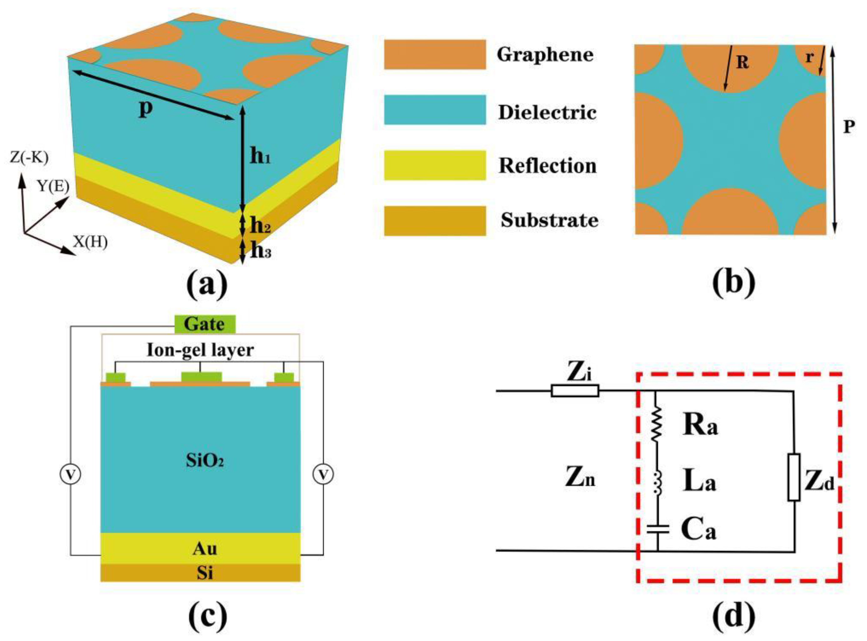
2. Structure and Method

We present a triple-band perfect absorber based on active tunable monolayer graphene in this paper. As shown in Figure 1a,b, the absorber unit structure is, from bottom to top, silicon substrate (thickness h3 = 0.1 μm), gold plane (thickness h2 = 0.25 μm), SiO2 layer (thickness h1 = 1 μm), and sector graphene layer. The radius of the major sector is 0.11 μm, and its origin is located in the center of the boundary. Similarly, the radius of the minor sector is 0.08 μm, which is located at the center of the corners. The graphene pattern layer is symmetrically centered and arranged in an orderly manner. The absorber basic unit has a periodic structure boundary, and the period P = 0.4 μm. In this structure, the refractive index of silicon dioxide is defined as 1.97, and the refractive index of silicon is defined as 3.34. They are used as nondestructive materials for the spacer layer and the silicon substrate, respectively [52]. The gold plane selects the depleted gold as the metal layer to participate in the plasmon resonance. Following the Drude conductance mode, the gold dielectric constant (εAu) can be described as: εAu = 9 − ω2p/(ω20 + iωγ). Among them, the work frequency of gold is ωp = 1.37 × 10¹⁶ s−1, while the collision coefficient is γ = 1.23 × 10¹⁴ s−1 [53]. The dielectric constant (ε) of graphene can be indicated by Equation (1) [54]:
ε(ω) = 1 + iσg/ω ε0
Among these, ω refers to the angular frequency of graphene, ε0 is the vacuum dielectric constant, ∆ is the thickness of graphene, and σg indicates the surface conductivity of graphene. In this paper, the graphene thickness is taken as 1 nm to facilitate numerical simulation and parameter convergence [55]. (We will explain the reason for taking 1 nm for the graphene thickness in the next section.) Second, the conductivity of graphene consists (σg) of two transitions, intraband transitions and interband transitions, and the formula is σg = σintra + σinter. Therefore, it can be inferred according to the Kubo formula that [56,57]:
σ intra ( ω ) = ie 2 K B T π h 2 ( ω + i τ 1 ) { E F K B T + 2 ln [ exp ( E F K B T ) + 1 ] }
σ inter ( ω ) = ie 2 4 π h 2 ln [ 2 | E F | h ( ω + i τ 1 ) 2 | E F | + h ( ω + i τ 1 ) ]
In the infrared and terahertz bands, the photon energy ħ ω E F . As a result, according to the Pauli incompatibility criterion, the interband transition conductivity σinter of graphene is negligible [58]. Therefore, the graphene surface conductivity can be approximately replaced by the intraband transition conductivity. Therefore, the equation for the conductivity of graphene can be simplified to the following form [59,60]:
σ ( ω ) = ie 2 π h 2 E F ( ω + i τ 1 )
where e is equal to the charge, EF is the Fermi level, ω is the angular frequency, τ is the relaxation time of the carrier, and the reduced Planck constant can be expressed as ħ = h / 2 π . During the simulation, we take Fermi level as 0.52 eV. We obtained the permittivity of graphene according to the above Equations (1)–(4). Then we imported the graphene material via a script file in the FDTD solution software. Furthermore, the article uses mid-infrared planar light vertically incident on the graphene layer at wavelengths of 2.5 to 4.15 μm, with a perfect match condition (PML) in the Z-axis [61]. Additionally, the periodic boundary conditions are used in both X and Y directions.
In the process of preparing a graphene plasmon resonance absorber, we deposited corresponding elements on a silicon substrate by electron beam evaporation technology, obtaining a suitable gold film and SiO2 spacer layer. Then, we gained the corresponding graphene layer on the surface of the SiO2 spacer layer by chemical vapor deposition (CVD) and wet transfer technology. Finally, we achieved the fan-shaped graphene pattern by lithography and electron beam. More detailed processing methods can be referred to [62,63].
According to the energy conservation formula, A (λ) +T (λ) +R (λ) = 1, where A (λ) is absorption efficiency, T (λ) is transmission, and R (λ) is reflectivity. We can obtain perfect absorption by reducing reflection and eliminating transmission. Fortunately, compared with the skin depth of the metal layer, the metal layer with a thickness of 0.25 μm can allow the incident light to be completely reflected without transmission. Therefore, the transmittance T (λ) = 0; that is, the absorptivity of a graphene resonance absorber can be simplified as A (λ) = 1 − R (λ).
Impedance matching is an important reference factor in measuring reflectivity and reducing reflection. In the theory of impedance matching, the formula can be used [64].
z = ( 1 + S 11 ) 2 S 21 2 ( 1 S 11 ) 2 S 21 2
S11 and S21 are reflected and transmitted complex amplitudes, respectively. Only when the equivalent surface impedance and space-free impedance are within the resonant frequency band can the system achieve effective impedance matching. The corresponding impedance values are Re(z) = 1 and Im(z) = 0 (i.e., the reflection complex amplitude S11 = 0), which means that the reflectivity R (λ) of the structure can be minimized. At the same time, the structure size is optimized and the related parameters are tuned to ensure the best spatial impedance. Figure 2 is the impedance matching diagram. When the real part Re(z) and imaginary part Im(z) are 1 and 0, respectively, low reflectivity is obtained. It means that the absorber can produce resonance absorption and perfect absorption peak.
In the above argument, we explained the conditions for the appearance of resonance peaks when the space-free impedance and the equivalent surface impedance are matched. Next, we further elaborated the computational theory of impedance matching from the perspective of the equivalent circuit model (ECM).
In the equivalent circuit model (see Figure 1d), the dielectric layer (silica) and the space-free impedance can be represented by Zd and Zi, respectively. The metallic layer Au acts as a zero-potential point and acts as a potential reference. The top-patterned graphene can be reduced to a series connection of resistive (Ra), inductive (La), and capacitive (Ca) components, where Ra and La are induced by the size sector graphene sheet and Ca is induced by the sector graphene gap. The impedance of the patterned graphene layers presented in the text is denoted by Zg. Zn denotes the input impedance. The reflection efficiency Γ of the absorber can be expressed as [65]:
Γ = Z n Z i Z i + Z n = Z n ( Z g , f ) Z i Z n ( Z g , f ) + Z i
Z n ( Z g , f ) = Z d ( f ) Z g ( f ) Z d ( f ) + Z g ( f )
Z d ( f ) = iZ 1 tan [ hk 1 ( f ) ] = i μ 0 / ε 0 ε d tan ( 2 π fh ε 0 ε d μ 0 )
Z g ( f ) = R a ( f ) + iX a ( f ) = R a ( f ) + i ( 2 π fL a 1 2 π fC a )
In the above equations, μ0, ε0, and εd denote the magnetic permeability, the relative permittivity of the free space, and the relative permittivity of the dielectric layer, respectively. Referring to the relevant literature [66,67,68], values are assigned to the relevant parameters. Ultimately, the absorption efficiency of the absorber (A) can be expressed as:
A = 1 Γ 2
Thus, we can calibrate or predict the perfect absorption wavelength of the designed absorber based on the transmission line model. In addition, Da et al. demonstrated that the results under the equivalent circuit model correlate well with those of the numerical model. The team also achieved an absorption efficiency of more than 95% [69]. Furthermore, Chen et al. designed and fabricated a microwave absorber based on the equivalent circuit model, achieving over 70% absorption efficiency [70]. The above experiments both confirm that the equivalent model is reliable.

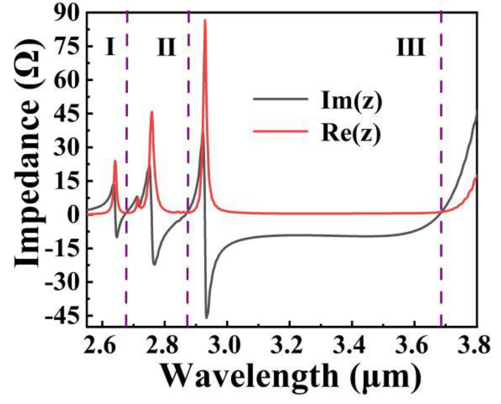
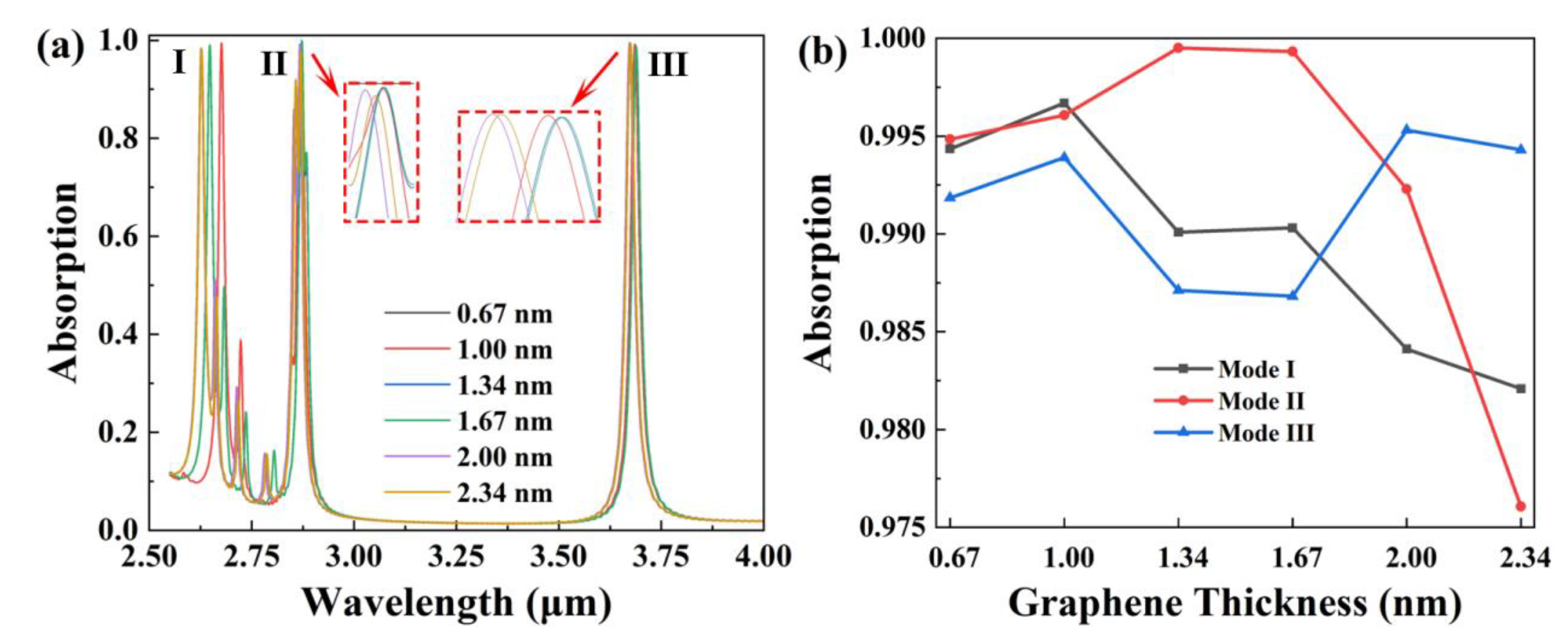
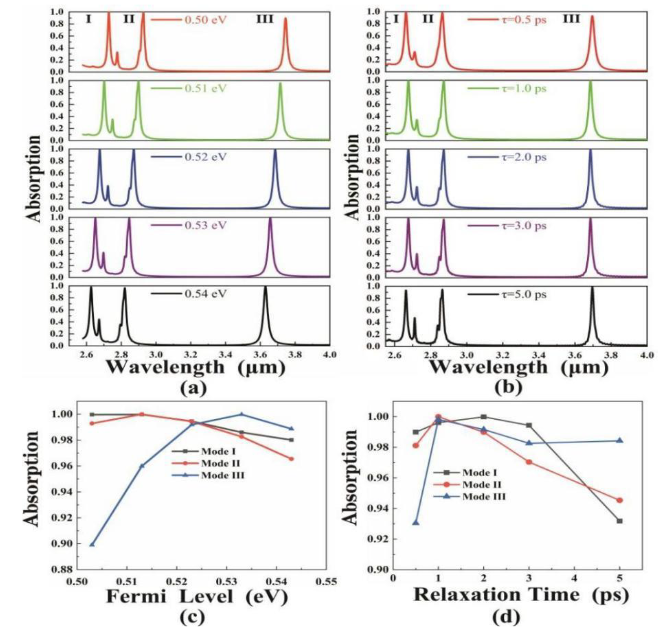
3. Results and Discussion

In the previous section, we calculated according to the two theories proposed above that good absorption peaks occur at wavelengths of 2.67, 2.87, and 3.68 μm, respectively. Next, we will validate the numerically simulated model by studying the cross-sectional electric field maps at the corresponding resonant wavelengths. Additionally, to better illustrate the peak characteristics in the article, we named the resonance peaks at 2.67, 2.87, and 3.68 μm as mode I, mode II, and mode III, respectively.
The Figure 3 shows the electromagnetic field distribution at wavelengths λ1 = 2.67 μm, λ2 = 2.87 μm, and λ3 = 3.68 μm. In this case, different colors represent the strength of the electric field localities. The first row shows the electric field localities of the absorber in the x–y plane. We can find that at a wavelength of 3.68 μm, the local resonance field range is very obvious, and we can clearly observe the EMF localities in the large sector arc. The second row shows the electric field of the cross section as observed in the y–z plane. We selected a planar observation window in the y–z plane at heights of 0.7 to 1.9 μm. At the corresponding waveband, we can clearly observe that mode 1 and mode 2 are generated by the slit of the sector and the internal localization of the small sector, respectively. Second, we can observe that the standing waves excited by the plasmon resonance are almost symmetric. This is the result of matching the surface impedance (Zn) and the space-free impedance (Zi) of the graphene layer and the dielectric layer together in this band. In this study, we focus on the excitation standing waves under the action of the graphene layer and the dielectric layer.
The mechanism is that the incident light will be reflected in the metal layer because it is not transmitted. When reflected light and incident light are repeatedly superimposed, standing waves will be formed in the patterned graphene layer. Finally, graphene generates a strong magnetic response and resonance absorption peak in the absorption spectrum.
In the previous section, we verified the peak position by observing the model cross-sectional electric field in simulation. Next, we will further discuss the assertion that the model has good tunability by adjusting parameters. However, it is necessary to clarify the reason why the graphene thickness is 1 nm in the simulation before formal discussion. In fact, the thickness of graphene was measured by reflection and contrast spectroscopy in reference [71], and the calculated results were in good agreement with the experimental results (error of 2%). That is, the thickness of a single layer of graphene should be 0.335 nm. However, the current experimental fabrication process of graphene is mainly obtained by chemical vapor deposition and wet transfer, which means that the obtained graphene layers are difficult to achieve a uniform single layer. In addition, if the graphene thickness is taken as 0.335 nm during the experimental simulation, the device will be distorted, which is not conductive to the subsequent simulation and actual fabrication. Therefore, the simulated thickness of graphene should be larger than 0.335 nm.
Therefore, as can be seen in Figure 4a, we simulated the influence of the resonance peak when the graphene thickness is 0.67, 1, 1.34, 1.67, 2, and 2.34 nm, respectively (the phenomenon of distortion occurred when the graphene thickness was 0.34 nm). The results show that the graphene thickness is insensitive to the excitation position of the mode, and the thickness mainly affects the absorption efficiency. According to Figure 4b, we can see that when the graphene thickness is 1 nm, the absorption efficiency of the three peaks is the highest on average. Therefore, the thickness of graphene is considered 1 nm in our simulations for subsequent studies.
To further explore the mechanism of the influence of the absorber, we explored the effect of geometrical parameters on the absorber. According to Figure 5 and Figure 6, on the premise that other conditions remain fixed, we separately discuss the influence of changing the radius of the minor sector and the major sector on the resonance absorption peak. The results in Figure 5 show that when the radius of minor sectors changed from 0.078 to 0.082 μm, the resonance absorption efficiency of mode I decreased from 99.95% to 93.57%, and that of mode II decreased from 98.8% to 94.58%, while mode III only fluctuated by 0.9%. This means that the influence of changing the radius of the minor sector on modes I and II is far greater than that on mode III.
The wavelengths in three modes, I–III, are only slightly blue-shifted 0.03 μm under the influence of the local electromagnetic field. This is because with the increase in the radius of the small sector, the effective arc length of the small sector increases, which weakens the local charge capacity of the minor sector. In this case, the coupling between different sectors is reduced, weakening the absorption efficiency. As mentioned above (mode III in Figure 3), the electromagnetic field of mode III is mainly localized in the arc segment of the major sector. Therefore, according to Figure 6a–c, when the radius of a major sector varies from 0.109 to 0.112 μm (when R is 0.107 μm, mode I is not within the range of mid-infrared band), the resonance absorption efficiencies of modes I and II fluctuated at 0.9% (mode I) and 0.7% (mode II), respectively, while that of mode III decreased from 98.29% to 94.38%. The specific reason is similar to the changing mechanism of a minor sector; that is, the substantial increase of effective arc length of a sector leads to the decrease in the local electromagnetic field capacity of a large sector. The situation eventually leads to a decrease in the absorption efficiency of mode III. Considering the red shift of the three modes, we find that the maximum fluctuation range of modes I and II is only 0.02 μm, while mode III moves at 0.08 μm. With the increase in the large sector radius, the effective arc segment increases, which changes the local electromagnetic field distribution and finally leads to the changes of the resonance region. Therefore, modes I–III red-shifted as a whole.
It is worth noting that with the slight changes in the shape of the patterned graphene, some smaller absorption peaks generate near the absorption peaks of Figure 5 (I–III). This is because the amount of electromagnetic field on the absorber is not infinite. Due to the boundary of the absorber, part of the electric field will leak, resulting in other absorption peaks [72].
According to Equations (1) and (4), the dielectric constant of graphene is greatly influenced by the Fermi level. In general, experiments usually employ modification of the external voltage or adjustment of the external light field to control the Fermi level of graphene. In our work, we alter the Fermi level of graphene by imposing an external voltage to the gold substrate. Figure 1c depicts a schematic diagram of the system for tuning the Fermi level of graphene. We previously placed metal electrodes on the graphene layer and coated it with a high-capacitance ionic gel. Next, we exerted an external voltage to change the carrier distribution between the ionic gel and graphene for the purpose of tuning the Fermi energy level. Moreover, a similar tuning method was experimentally verified in the literature [73], which demonstrates the feasibility of the scheme. According to the principle of Equation (11), we investigate the effect of the Fermi energy level on an absorber by controlling the external voltage of graphene [74].
E F = V f π ε 0 ε r V g e 0 t d
Among them, the thickness of the dielectric layer td = 1.5 μm, the Fermi velocity Vf = c/300, Vg is the applied voltage, charge e0 = 1.60 × 10⁻¹⁹ C, and εg is the relative permittivity. In this paper, the Fermi level of graphene is modified by revising the applied voltage Vg of graphene. Finally, we observe and discuss the absorption peak diagram intuitively. Figure 7a depicts the Fermi level absorption diagram when EF is superimposed from 0.50 to 0.54 eV on the premise that the incident infrared light reaches 0.01 eV. It is clear that modes I to III are blue-shifted as the Fermi level increases (see Figure 7a). It is easy to conclude after analysis that this is the result of changes in the local resonance regions of the electric and magnetic dipoles. The local resonance of the magnetic and electric dipoles is controlled by the equivalent circuit model, and the resonance frequency ωres can be expressed by Equation (12) [75,76]:
ω res = L a C a
In Equation (12), La and Ca refer to the effective inductance and capacitance, respectively (Figure 1d). The increases in the Fermi level can effectively promote the increases in carrier concentration, thus leading to the enhancement of the local electromagnetic field capacity of graphene, strengthening the resonance absorption of the absorber [77]. On the contrary, the increases in the Fermi level reduce the effective inductive reactance (L), and the corresponding formant frequency side length and wavelength become shorter. When the wavelength is out of the resonance region, the corresponding formant absorption peak will decrease. Therefore, the absorption efficiency of the three resonant peaks corresponding to Figure 7c shows a similar trend of rising first and then falling as the Fermi level increases.
Modifying the relaxation time is another way to alter graphene carrier absorption, which is based on the following formula [78]:
τ = E F υ / ( e υ F 2 )
In Equation (13), the Fermi velocity is VF = 106 m/s, the charge is e0 = 1.60 × 10⁻¹⁹ J/s, and the carrier mobility of graphene is υ. The carrier mobility υ can be changed by means of electrostatic gating or chemical doping so as to explore the corresponding situation of relaxation time on the absorption of graphene carriers. In this paper, the Fermi energy level was fixed at 0.52 eV. By placing organic molecules on the surface of graphene, we can improve the absorption surface properties of graphene, for example, by doping organic molecules, such as F4-TCNQ and TCNE [79]. According to the simulation results obtained by FDTD, we can finally view the condition of absorption peaks in Figure 7b,d. The results show that the relaxation time has a tiny effect on the absorption efficiency. When the relaxation time (τ) varied from 0.5 to 5 ps, the absorption peaks varied from 99.98% to 93.17% (mode I), 99.99% to 94.53% (mode II), 99.82% to 93.04% (mode III). Figure 7d shows that the three resonant absorption peaks increase first and then decrease with the increases in relaxation time. The specific reasons are as follows: the increases of relaxation time promote the improvement of graphene carrier mobility and greatly enhance the probability of surface plasmon resonance. When the surface plasmon oscillation approaches saturation, as the relaxation time continues to increase, most of the light will be reflected, and the absorption efficiency will decrease correspondingly, and the overall trend tends to decline. For the three modes, the resonance wavelengths almost remain about 2.67 μm (mode I), 2.87 μm (mode II), and 3.68 μm (mode III). This is because the wavelength excited by the magnetic dipole resonance is not sensitive to the circular pattern of sector graphene.
Excellent absorbers must have strong environmental adaptability to have a broader application space. Therefore, it is particularly significant to study the polarization absorption of the absorber under transverse electric (TE) waves and transverse magnetic (TM) waves. According to Figure 8a, under the premise of two polarizations with normally incident conditions, highly consistent absorption curves corresponding to the three modes were obtained. The polarization insensitivity of our model is attributed to the symmetry of the absorber unit structure [80]. In order to better illustrate the polarization insensitivity of the model, we focus on the reflection versus transmission of the observed model and plot it (see Figure 8b). We find that the good absorption performance of the model is due to the fact that at vertical incidence, the transmission of the model is 0. The absorption is therefore linearly related to the reflection. The above results show that the absorber has good adaptability to polarized waves incident perpendicularly in different directions.
In addition, it is important to study the stability of absorber resonance absorption at different incident angles. From Figure 9a,b, with the increase in incident angle, the resonance absorption peaks of the three modes can maintain high absorption within the wide incident angle range of 0°–45°. For the TM wave, both mode I and mode II can maintain high absorption between 0° and 50°, while mode III is slightly affected by the polarization angle. This is because the TM wave excited by the longitudinal component of the electric field has different sensitivity to the incident light in different places due to the influence of the local electromagnetic field distribution. Eventually, part of the electric field will weaken with the increases in incident angle, or even be destroyed. It results in the failure of the corresponding resonance absorption peak. Similarly, for the TE wave, mode I can maintain high absorption at 0°–50°, mode II has a slight blue shift, and mode III can maintain high absorption at 0°–45°. The phenomenon of blue shift is mainly attributed to the destruction of the graphene LSPR. An excessively large incident angle reduces the effective refractive index of the light source, which ultimately affects the localization of the resonant absorption peak. In conclusion, the graphene plasmon resonance absorber maintains a high absorption efficiency at an incident angle of 0°–45°, which to some extent promotes the application expansion of the absorber in photodetectors, biochemical sensors, and other fields.

4. Conclusions

In summary, a triple-band perfect absorber based on active tunable monolayer graphene is proposed in this paper. The simulation results show that the perfect absorption is achieved at three mid-infrared wave bands at λ1 = 2.67 μm, λ2 = 2.87 μm, and λ3 = 3.68 μm. In the process of parameter tuning, the absorption efficiency and wavelength of resonance peaks can be optimized by modifying geometric parameters. In addition, the characteristics of the absorber can be flexibly regulated by adjusting the Fermi level. Modifying the relaxation time only affects the absorption efficiency of the absorber, but has no effect on the resonance wavelength. The absorber also has good absorption performance at a large incident angle up to 45°. Moreover, the symmetrical structure makes the absorber insensitive to polarization, which greatly extends the application of the absorber.

Author Contributions

Conceptualization, H.R., Q.S. and Z.S.; data curation, H.R., Y.Z. and Z.Y.; formal analysis, H.R. and G.M.; methodology, J.Z., H.Y., S.W., P.W., Z.Y. and G.M.; resources, H.Y.; software, H.R., Y.Z., Z.Y. and P.W.; data curation, H.R.; writing—original draft preparation, Y.Z.; writing—review and editing, H.R., H.Y., S.W. and P.W. All authors have read and agreed to the published version of the manuscript.

Funding

The authors are grateful for the support of the National Natural Science Foundation of China (nos. 51606158, 11604311, 61705204, 21506257), funded by the Scientific Research Fund of Si Chuan Provincial Science and Technology Department (2020YJ0137, 2020YFG0467, 2021JDRC0019), Open Fund of the Key Laboratory for Metallurgical Equipment and Control Technology of the Ministry of Education at the Wuhan University of Science and Technology (no. MECOF2020B02), Undergraduate Innovation Fund Project Precision Funding of Southwest University of Science and Technology (no. JZ20-025), college students’ innovation and entrepreneurship training program (S202110619073, S202110619069, S202110619100), Postgraduate Innovation Fund Project of Southwest University of Science and Technology (no. 18ycx034), and Southwest University of Science and Technology Students Innovation Fund project (no. CX20-031).

Institutional Review Board Statement

Not applicable.

Informed Consent Statement

Not applicable.

Data Availability Statement

Publicly available datasets were analyzed in this study. These data can be found at [https://www.lumerical.com/ (accessed on 27 April 2022)].

Conflicts of Interest

The authors declare no conflict of interest.

References

  1. Schurig, D.; Mock, J.J.; Justice, B.J.; Cummer, S.A.; Pendry, J.B.; Starr, A.F.; Smith, D.R. Metamaterial Electromagnetic Cloak at Microwave Frequencies. Science 2006, 314, 977–980. [Google Scholar] [CrossRef] [Green Version]
  2. Chen, J.; Nie, H.; Tang, C.; Cui, Y.; Yan, B.; Zhang, Z.; Kong, Y.; Xu, Z.; Cai, P. Highly sensitive refractive-index sensor based on strong magnetic resonance in metamaterials. Appl. Phys. Express 2019, 12, 052015. [Google Scholar] [CrossRef]
  3. Cheng, T.; Gao, H.; Liu, G.; Pu, Z.; Wang, S.; Yi, Z.; Wu, X.; Yang, H. Preparation of core-shell heterojunction photocatalysts by coating CdS nanoparticles onto Bi4Ti3O12 hierarchical microspheres and their photocatalytic removal of organic pollutants and Cr(VI) ions. Colloids Surfaces A Physicochem. Eng. Asp. 2021, 633, 127918. [Google Scholar] [CrossRef]
  4. Zheng, Z.; Luo, Y.; Yang, H.; Yi, Z.; Zhang, J.; Song, Q.; Yang, W.; Liu, C.; Wu, X.; Wu, P. Thermal tuning of terahertz metamaterial properties based on phase change material vanadium dioxide. Phys. Chem. Chem. Phys. 2022, 24, 8846–8853. [Google Scholar] [CrossRef]
  5. Li, L.; Gao, H.; Liu, G.; Wang, S.; Yi, Z.; Wu, X.; Yang, H. Synthesis of carnation flower-like Bi2O2CO3 photocatalyst and its promising application for photoreduction of Cr(VI). Adv. Powder Technol. 2022, 33, 103481. [Google Scholar] [CrossRef]
  6. Manjappa, M.; Srivastava, Y.K.; Solanki, A.; Kumar, A.; Sum, T.C.; Singh, R. Hybrid Lead Halide Perovskites for Ultrasensitive Photoactive Switching in Terahertz Metamaterial Devices. Adv. Mater. 2017, 29, 1605881. [Google Scholar] [CrossRef]
  7. Wu, X.; Zheng, Y.; Luo, Y.; Zhang, J.; Yi, Z.; Wu, X.; Cheng, S.; Yang, W.; Yu, Y.; Wu, P. A four-band and polarization-independent BDS-based tunable absorber with high refractive index sensitivity. Phys. Chem. Chem. Phys. 2021, 23, 26864–26873. [Google Scholar] [CrossRef]
  8. Zheng, Y.; Wu, P.; Yang, H.; Yi, Z.; Luo, Y.; Liu, L.; Song, Q.; Pan, M.; Zhang, J.; Cai, P. High efficiency Titanium oxides and nitrides ultra-broadband solar energy absorber and thermal emitter from 200 nm to 2600 nm. Opt. Laser Technol. 2022, 150, 108002. [Google Scholar] [CrossRef]
  9. Li, L.; Gao, H.; Yi, Z.; Wang, S.; Wu, X.; Li, R.; Yang, H. Comparative investigation on synthesis, morphological tailoring and photocatalytic activities of Bi2O2CO3 nanostructures. Colloids Surfaces A Physicochem. Eng. Asp. 2022, 644, 128758. [Google Scholar] [CrossRef]
  10. Li, L.; Sun, X.; Xian, T.; Gao, H.; Wang, S.; Yi, Z.; Wu, X.; Yang, H. Template-free synthesis of Bi2O2CO3 hierarchical nanotubes self-assembled from ordered nanoplates for promising photocatalytic applications. Phys. Chem. Chem. Phys. 2022, 24, 8279–8295. [Google Scholar] [CrossRef]
  11. Landy, N.I.; Sajuyigbe, S.; Mock, J.J.; Smith, D.R.; Padilla, W.J. Perfect Metamaterial Absorber. Phys. Rev. Lett. 2008, 100, 207402. [Google Scholar] [CrossRef]
  12. Li, J.; Jiang, J.; Xu, Z.; Liu, M.; Tang, S.; Yang, C.; Qian, D. Facile synthesis of Ag@Cu2O heterogeneous nanocrystals decorated N-doped reduced graphene oxide with enhanced electrocatalytic activity for ultrasensitive detection of H2O2. Sens. Actuators B Chem. 2018, 260, 529–540. [Google Scholar] [CrossRef]
  13. Li, Y.; Li, M.; Xu, P.; Tang, S.; Liu, C. Efficient photocatalytic degradation of acid orange 7 over N-doped ordered mesoporous titania on carbon fibers under visible-light irradiation based on three synergistic effects. Appl. Catal. A Gen. 2016, 524, 163–172. [Google Scholar] [CrossRef]
  14. Xiong, S.; Yin, Z.; Zhou, Y.; Peng, X.; Yan, W.; Liu, Z.; Zhang, X. The Dual-frequency (20/40 kHz) Ultrasound Assisted Photocatalysis with the Active Carbon Fiber-loaded Fe3+-TiO2as Photocatalyst for Degradation of Organic Dye. Bull. Korean Chem. Soc. 2013, 34, 3039–3045. [Google Scholar] [CrossRef] [Green Version]
  15. Tang, N.; Li, Y.; Chen, F.; Han, Z. In situ fabrication of a direct Z-scheme photocatalyst by immobilizing CdS quantum dots in the channels of graphene-hybridized and supported mesoporous titanium nanocrystals for high photocatalytic performance under visible light. RSC Adv. 2018, 8, 42233–42245. [Google Scholar] [CrossRef] [Green Version]
  16. Chen, H.-J.; Zhang, Z.-H.; Cai, R.; Kong, X.-Q.; Chen, X.; Liu, Y.-N.; Yao, S.-Z. Molecularly imprinted electrochemical sensor based on a reduced graphene modified carbon electrode for tetrabromobisphenol A detection. Analyst 2013, 138, 2769–2776. [Google Scholar] [CrossRef]
  17. Tao, H.; Bingham, C.M.; Pilon, D.; Fan, K.; Strikwerda, A.C.; Shrekenhamer, D.; Padilla, W.J.; Zhang, X.; Averitt, R.D. A dual band terahertz metamaterial absorber. J. Phys. D Appl. Phys. 2010, 43, 225102. [Google Scholar] [CrossRef]
  18. Fan, Y.; Zhang, F.; Zhao, Q.; Wei, Z.; Li, H. Tunable terahertz coherent perfect absorption in a monolayer graphene. Opt. Lett. 2014, 39, 6269–6272. [Google Scholar] [CrossRef] [Green Version]
  19. Zhao, F.; Lin, J.; Lei, Z.; Yi, Z.; Qin, F.; Zhang, J.; Liu, L.; Wu, X.; Yang, W.; Wu, P. Realization of 18.97% theoretical efficiency of 0.9 μm thick c-Si/ZnO heterojunction ultrathin-film solar cells via surface plasmon resonance enhancement. Phys. Chem. Chem. Phys. 2022, 24, 4871–4880. [Google Scholar] [CrossRef]
  20. Dayal, G.; Ramakrishna, S.A. Design of highly absorbing metamaterials for infrared frequencies. Opt. Express 2012, 20, 17503–17508. [Google Scholar] [CrossRef]
  21. Wang, J.X.; Cheng, Y.Z.; Luo, H.; Chen, F.; Wu, L. High-gain bidirectional radiative circularly polarized antenna based on focusing metasurface. Int. J. Electron. Commun. 2022, 151, 154222. [Google Scholar] [CrossRef]
  22. Yan, Z.; Lu, X.; Du, W.; Lv, Z.; Tang, C.; Cai, P.; Gu, P.; Chen, J.; Yu, Z. Ultraviolet graphene ultranarrow absorption engineered by lattice plasmon resonance. Nanotechnology 2021, 32, 465202. [Google Scholar] [CrossRef]
  23. Zheng, Z.; Zheng, Y.; Luo, Y.; Yi, Z.; Zhang, J.; Liu, Z.; Yang, W.; Yu, Y.; Wu, X.; Wu, P. A switchable terahertz device combining ultra-wideband absorption and ultra-wideband complete reflection. Phys. Chem. Chem. Phys. 2022, 24, 2527–2533. [Google Scholar] [CrossRef]
  24. Ren, Y.; Zhou, T.L.; Jiang, C.; Tang, B. Thermally switching between perfect absorber and asymmetric transmission in vanadium diox-ide-assisted metamaterials. Opt. Express 2021, 29, 7666–7679. [Google Scholar]
  25. Zhou, F.; Qin, F.; Yi, Z.; Yao, W.-T.; Liu, Z.; Wu, X.; Wu, P. Ultra-wideband and wide-angle perfect solar energy absorber based on Ti nanorings surface plasmon resonance. Phys. Chem. Chem. Phys. 2021, 23, 17041–17048. [Google Scholar] [CrossRef]
  26. Haque, E.; Mahmuda, S.; Hossain, A.; Hai, N.H.; Namihira, Y.; Ahmed, F. Highly Sensitive Dual-Core PCF Based Plasmonic Refractive Index Sensor for Low Refractive Index Detection. IEEE Photonics J. 2019, 11, 5. [Google Scholar] [CrossRef]
  27. Jiang, L.; Yi, Y.; Tang, Y.; Li, Z.; Yi, Z.; Liu, L.; Chen, X.; Jian, R.; Wu, P.; Yan, P. A high quality factor ultra-narrow band perfect metamaterial absorber for monolayer molybdenum disulfide. Chin. Phys. B 2022, 31, 038101. [Google Scholar]
  28. Zhu, X.Z.; Cheng, Y.Z.; Fan, J.P.; Chen, F.; Luo, H.; Wu, L. Switchable efficiency terahertz anomalous refraction and focusing based on graphene metasurface. Diam. Relat. Mater. 2022, 121, 108743. [Google Scholar] [CrossRef]
  29. Novoselov, K.S.; Geim, A.K.; Morozov, S.V.; Jiang, D.; Zhang, Y.; Dubonos, S.V.; Grigorieva, I.V.; Firsov, A.A. Electric field effect in atomically thin carbon films. Science 2004, 306, 666–669. [Google Scholar]
  30. Xu, W.; Xie, L.; Ying, Y. Mechanisms and applications of terahertz metamaterial sensing: A review. Nanoscale 2017, 9, 13864–13878. [Google Scholar] [CrossRef]
  31. Chen, H.; Chen, Z.; Yang, H.; Wen, L.; Yi, Z.; Zhou, Z.; Dai, B.; Zhang, J.; Wu, X.; Wu, P. Multi-mode surface plasmon resonance absorber based on dart-type single-layer graphene. RSC Adv. 2022, 12, 7821–7829. [Google Scholar] [CrossRef]
  32. Cai, L.; Zhang, Z.; Xiao, H.; Chen, S.; Fu, J. An eco-friendly imprinted polymer based on graphene quantum dots for fluorescent detection of p-nitroaniline. RSC Adv. 2019, 9, 41383–41391. [Google Scholar] [CrossRef] [Green Version]
  33. Long, F.; Zhang, Z.H.; Wang, J.; Yan, L.; Lu, P.P.; Yang, Z.X. Magnetic graphene modified imprinted electrochemical sensor for detection of 4-Octylphenol. Chin. J. Anal. Chem. 2016, 44, 908–914. [Google Scholar]
  34. Ferreira, A.; Peres, N.M.R. Complete light absorption in graphene-metamaterial corrugated structures. Phys. Rev. B 2012, 86, 205401. [Google Scholar] [CrossRef] [Green Version]
  35. Zhang, C.; Yi, Y.; Yang, H.; Yi, Z.; Chen, X.; Zhou, Z.; Yi, Y.; Li, H.; Chen, J.; Liu, C. Wide spectrum solar energy absorption based on germanium plated ZnO nanorod arrays: Energy band regulation, Finite element simulation, Super hydrophilicity, Photothermal conversion. Appl. Mater. Today 2022, 28, 101531. [Google Scholar] [CrossRef]
  36. Long, F.; Zhang, Z.; Wang, J.; Yan, L.; Zhou, B. Cobalt-nickel bimetallic nanoparticles decorated graphene sensitized imprinted electrochemical sensor for determination of octylphenol. Electrochim. Acta 2015, 168, 337–345. [Google Scholar] [CrossRef]
  37. Fang, Z.; Wang, Y.; Schlather, A.E.; Liu, Z.; Ajayan, P.M.; de Abajo, F.J.G.; Nordlander, P.; Zhu, X.; Halas, N.J. Active Tunable Absorption Enhancement with Graphene Nanodisk Arrays. Nano Lett. 2013, 14, 299–304. [Google Scholar] [CrossRef]
  38. Zhang, Z.; Cai, R.; Long, F.; Wang, J. Development and application of tetrabromobisphenol A imprinted electrochemical sensor based on graphene/carbon nanotubes three-dimensional nanocomposites modified carbon electrode. Talanta 2015, 134, 435–442. [Google Scholar] [CrossRef]
  39. Grady, N.K.; Heyes, J.E.; Chowdhury, D.R.; Zeng, Y.; Reiten, M.T.; Azad, A.K.; Taylor, A.J.; Dalvit, D.A.R.; Chen, H.-T. Terahertz Metamaterials for Linear Polarization Conversion and Anomalous Refraction. Science 2013, 340, 1304–1307. [Google Scholar] [CrossRef] [Green Version]
  40. Zhou, J.; Koschny, T.; Soukoulis, C.M. An efficient way to reduce losses of left-handed metamaterials. Opt. Express 2008, 16, 11147–11152. [Google Scholar] [CrossRef] [Green Version]
  41. Plum, E.; Fedotov, V.A.; Kuo, P.; Tsai, D.P.; Zheludev, N.I. Towards the lasing spaser: Controlling metamaterial optical response with semi-conductor quantum dots. Opt. Express 2009, 17, 8548–8551. [Google Scholar]
  42. Zou, H.; Cheng, Y. Design of a six-band terahertz metamaterial absorber for temperature sensing application. Opt. Mater. 2019, 88, 674–679. [Google Scholar] [CrossRef]
  43. Li, R.; Zheng, Y.; Luo, Y.; Zhang, J.; Yi, Z.; Liu, L.; Song, Q.; Wu, P.; Yu, Y.; Zhang, J. Multi-peak narrow-band perfect absorber based on two-dimensional graphene array. Diam. Relat. Mater. 2021, 120, 108666. [Google Scholar] [CrossRef]
  44. Shen, X.; Yang, Y.; Zang, Y.; Gu, J.; Han, J.; Zhang, W.; Cui, T.J. Triple-band terahertz metamaterial absorber: Design, experiment, and physical interpretation. Appl. Phys. Lett. 2012, 101, 154102. [Google Scholar] [CrossRef]
  45. Huang, X.; Pan, K.; Hu, Z. Experimental Demonstration of Printed Graphene Nano-flakes Enabled Flexible and Conformable Wideband Radar Absorbers. Sci. Rep. 2016, 6, 38197. [Google Scholar] [CrossRef]
  46. Alireza, S.; Abraham, V.G.; Jean, C.; Daniel, F.; Laurene, T.; Zhai, L.; Michael, N.L.; Debashis, C. Dynamically tunable extraordinary light absorption in monolayer graphene. Phys. Rev. B 2017, 96, 165431. [Google Scholar]
  47. Jiang, L.-Y.; Yi, Y.-T.; Yi, Z.; Yang, H.; Li, Z.-Y.; Su, J.; Zhou, Z.-G.; Chen, X.-F.; Yi, Y.-G. A four-band perfect absorber based on high quality factor and high figure of merit of monolayer molybdenum disulfide. Acta Phys. Sin. 2021, 70, 128101. [Google Scholar] [CrossRef]
  48. Liao, Y.-L.; Zhao, Y. Graphene-based tunable ultra-narrowband mid-infrared TE-polarization absorber. Opt. Express 2017, 25, 32080–32089. [Google Scholar] [CrossRef]
  49. Barzegar-Parizi, S. Realization of wide-angle and wideband absorber using metallic and graphene-based metasurface for mid-infrared and low THz frequency. Opt. Quantum Electron. 2018, 50, 378. [Google Scholar] [CrossRef]
  50. Meng, H.; Wang, L.; Liu, G.; Xue, X.; Lin, Q.; Zhai, X. Tunable graphene-based plasmonic multispectral and narrowband perfect metamaterial absorbers at the mid-infrared region. Appl. Opt. 2017, 56, 6022–6027. [Google Scholar] [CrossRef]
  51. Fardoost, A.; Vanani, F.G.; Amirhosseini, S.A.; Safian, R. Design of Multi-Layer Graphene Based Ultra Wideband Terahertz Absorber. IEEE Trans. Nanotechnol. 2016, 16, 68–74. [Google Scholar] [CrossRef]
  52. Yi, Z.; Li, J.; Lin, J.; Qin, F.; Chen, X.; Yao, W.; Liu, Z.; Cheng, S.; Wu, P.; Li, H. Broadband polarization-insensitive and wide-angle solar energy absorber based on tungsten ring-disc array. Nanoscale 2020, 12, 23077–23083. [Google Scholar] [CrossRef]
  53. Li, J.; Chen, X.; Yi, Z.; Yang, H.; Tang, Y.; Yi, Y.; Yao, W.; Wang, J.; Yi, Y. Broadband solar energy absorber based on monolayer molybdenum disulfide using tungsten elliptical arrays. Mater. Today Energy 2020, 16, 100390. [Google Scholar] [CrossRef]
  54. Lin, X.; Li, Y.J.; Chen, F.T.; Xu, P.; Li, M. Facile synthesis of mesoporous titanium dioxide doped by Ag-coated graphene with enhanced visible-light photocatalytic performance for methylene blue degradation. RSC Adv. 2017, 7, 25314–25324. [Google Scholar] [CrossRef] [Green Version]
  55. Xiao, S.; Wang, T.; Liu, T.; Yan, X.; Li, Z.; Xu, C. Active modulation of electromagnetically induced transparency analogue in terahertz hybrid metal-graphene metamaterials. Carbon 2018, 126, 271–278. [Google Scholar] [CrossRef] [Green Version]
  56. Lv, P.; Xie, D.; Zhang, Z. Magnetic carbon dots based molecularly imprinted polymers for fluorescent detection of bovine hemoglobin. Talanta 2018, 188, 145–151. [Google Scholar] [CrossRef]
  57. Long, F.; Wang, J.; Zhang, Z.; Yan, L. Magnetic imprinted electrochemical sensor combined with magnetic imprinted solid-phase extraction for rapid and sensitive detection of tetrabromobisphenol S. J. Electroanal. Chem. 2016, 777, 58–66. [Google Scholar] [CrossRef]
  58. Cai, R.; Rao, W.; Zhang, Z.; Long, F.; Yin, Y. An imprinted electrochemical sensor for bisphenol A determination based on electrodeposition of a graphene and Ag nanoparticle modified carbon electrode. Anal. Methods 2014, 6, 1590–1597. [Google Scholar] [CrossRef]
  59. Vorobieva, Y.; González-Hernández, J.; Vorobiev, P.; Bulat, L. Thermal-photovoltaic solar hybrid system for efficient solar energy conversion. Sol. Energy 2006, 80, 170–176. [Google Scholar]
  60. Cheng, Z.; Liao, J.; He, B.; Zhang, F.; Zhang, F.; Huang, X.; Zhou, L. One-Step Fabrication of Graphene Oxide Enhanced Magnetic Composite Gel for Highly Efficient Dye Adsorption and Catalysis. ACS Sustain. Chem. Eng. 2015, 3, 1677–1685. [Google Scholar] [CrossRef]
  61. Li, J.; Jiang, J.; Zhao, D.; Xu, Z.; Liu, M.; Liu, X.; Tong, H.; Qian, D. Novel hierarchical sea urchin-like Prussian blue@palladium core–shell heterostructures supported on nitrogen-doped reduced graphene oxide: Facile synthesis and excellent guanine sensing performance. Electrochim. Acta 2020, 330, 135196. [Google Scholar] [CrossRef]
  62. Mermin, N.D. Crystalline Order in Two Dimensions. Phys. Rev. 1968, 176, 250. [Google Scholar] [CrossRef]
  63. Qin, F.; Chen, X.; Yi, Z.; Yao, W.; Yang, H.; Tang, Y.; Yi, Y.; Li, H.; Yi, Y. Ultra-broadband and wide-angle perfect solar absorber based on TiN nanodisk and Ti thin film structure. Sol. Energy Mater. Sol. Cells 2020, 211, 110535. [Google Scholar] [CrossRef]
  64. Cao, G.; Li, H.; Deng, Y.; Zhan, S.; He, Z.; Li, B. Systematic Theoretical Analysis of Selective-Mode Plasmonic Filter Based on Aperture-Side-Coupled Slot Cavity. Plasmonics 2014, 9, 1163–1169. [Google Scholar] [CrossRef]
  65. Liu, H.; Wang, Q.; Zhang, F. Preparation of Fe3O4@SiO2@ P(AANa-co-AM) Composites and Their Adsorption for Pb(II). ACS Omega 2020, 5, 8816–8824. [Google Scholar] [CrossRef] [Green Version]
  66. Kamran, J.J.; Maryam, A.; Tayebeh, A.; Mohammad, B.; Sadegh, B. Multi-bias, graphene-based reconfigurable THz absorber/reflector. Optik 2019, 198, 163248. [Google Scholar]
  67. Chen, P.; Alù, A. Terahertz Metamaterial Devices Based on Graphene. Nanostruct. IEEE Trans. Terahertz. Sci. Technol. 2013, 3, 748–756. [Google Scholar]
  68. Mishra, R.; Sahu, A.; Panwar, R. Cascaded Graphene Frequency Selective Surface Integrated Tunable Broadband Terahertz Metamaterial Absorber. IEEE Photonics J. 2019, 11, 2200310. [Google Scholar] [CrossRef]
  69. Yi, D.; Wei, X.; Xu, Y. Experimental demonstration of transparent microwave absorber based on graphene. In Proceedings of the 2016 IEEE MTT-S International Wireless Symposium (IWS), Shanghai, China, 14–16 March 2016; pp. 1–4. [Google Scholar] [CrossRef]
  70. Chen, H.; Huang, Y.; Li, G.; He, Q.; Xie, J.; Deng, L. Design and experimental validation of a low-profile wideband metamaterial absorber by characteristic modes analysis. Results Phys. 2021, 28, 104684. [Google Scholar] [CrossRef]
  71. Ni, Z.H.; Wang, H.M.; Kasim, J.; Fan, H.M.; Yu, T.; Wu, Y.H.; Feng, Y.P.; Shen, Z.X. Graphene Thickness Determination Using Reflection and Contrast Spectroscopy. Nano Lett. 2007, 7, 2758–2763. [Google Scholar] [CrossRef]
  72. Chen, P.; Liu, F.; Ding, H.; Chen, S.; Chen, L.; Li, Y.-J.; Au, C.-T.; Yin, S.-F. Porous double-shell CdS@C3N4 octahedron derived by in situ supramolecular self-assembly for enhanced photocatalytic activity. Appl. Catal. B Environ. 2019, 252, 33–40. [Google Scholar] [CrossRef]
  73. Yang, X.; Zhang, F.; Hu, Y.J.; Chen, D.Z.; He, Z.Q.; Xiong, L.Z. Gold nanoparticals doping graphene sheets nanocomposites sensitized screen-printed carbon electrode as a disposable platform for voltammetric determination of guaiacol in bamboo juice. Int. J. Electrochem. Sci. 2014, 9, 5061–5072. [Google Scholar]
  74. Shreyas, C.; Shobhit, K.P.; Krishna, D.; Rajendrasinh, J.; Truong, K.N.; Vigneswaran, D. Numerical investigation of wideband L-shaped metasurface based solar absorber for visible and ultraviolet region. Phys. B Condens. Matter 2021, 601, 412503. [Google Scholar]
  75. Liu, Y.; Bo, M.; Yang, X.; Zhang, P.; Sun, C.Q.; Huang, Y. Size modulation electronic and optical properties of phosphorene nanoribbons: DFT–BOLS approximation. Phys. Chem. Chem. Phys. 2017, 19, 5304–5309. [Google Scholar] [CrossRef]
  76. Deng, Y.; Cao, G.; Yang, H.; Zhou, X.; Wu, Y. Dynamic Control of Double Plasmon-Induced Transparencies in Aperture-Coupled Waveguide-Cavity System. Plasmonics 2018, 13, 345–352. [Google Scholar] [CrossRef]
  77. Deng, Y.; Cao, G.; Wu, Y.; Zhou, X.; Liao, W. Theoretical Description of Dynamic Transmission Characteristics in MDM Waveguide Aperture-Side-Coupled with Ring Cavity. Plasmonics 2015, 10, 1537–1543. [Google Scholar] [CrossRef]
  78. Qu, Y.; Li, Q.; Gong, H.; Du, K.; Bai, S.; Zhao, D.; Ye, H.; Qiu, M. Spatially and Spectrally Resolved Narrowband Optical Absorber Based on 2D Grating Nanostructures on Metallic Films. Adv. Opt. Mater. 2016, 4, 480–486. [Google Scholar] [CrossRef]
  79. Chen, W.; Chen, S.; Qi, D.C.; Gao, X.Y.; Wee, A.T.S. Surface Transfer p-Type Doping of Epitaxial Graphene. J. Am. Chem. Soc. 2007, 129, 10418–10422. [Google Scholar] [CrossRef]
  80. Gao, E.; Liu, Z.; Li, H.; Xu, H.; Zhang, Z.; Luo, X.; Xiong, C.; Liu, C.; Zhang, B.; Zhou, F. Dynamically tunable dual plasmon-induced trans-parency and absorption based on a single-layer patterned graphene metamaterial. Opt. Express 2019, 27, 13884–13894. [Google Scholar]
Figure 1. (a) Diagram of the graphene plasma absorber structure unit. The structural units are, from top to bottom, the reactive layer graphene, the dielectric layer silica (h1 = 1 μm), the reflective layer gold plane (h2 = 0.25 μm), and the silicon substrate as physical support (h3 = 0.1 μm). (b) Schematic diagram of the graphene-patterned layer structure, where the structural unit period P = 0.4 μm, the large sector radius R = 0.11 μm, and the small sector radius r = 0.08 μm. (c) Diagram of the shared model for building the equivalent circuit and tuning the Fermi energy level. (d) Diagram of the RLC equivalent circuit of our model. The impedance of the dielectric layer (silica) and the space-free impedance can be expressed by Zd and Zi, respectively. Zn is the equivalent impedance. The metal layer Au acts as a zero potential point and as a potential reference. Ra, La, and Ca are the resistances, capacitances, and inductances of the sector graphene layer, respectively.
Coatings 12 00990 g001
Figure 2. The matching diagram of absorber impedance changing with wavelength when other parameters are fixed. The black line represents the imaginary part Im(z) of the impedance, and the red line represents the real part Re(z) of the impedance. When Im(z) and Re(z) are matched (Im(z) = 0, Re(z) = 1), the wavelengths corresponding to the optimal impedance values of modes I, II, and III are located at the dotted line.
Coatings 12 00990 g002
Figure 3. Modes (I)~(III) show the electric field distribution of the x–y plane (a) and y–z plane (b) of the graphene plasmon absorber at λ1 = 2.67 μm, λ2 = 2.87 μm, and λ3 = 3.68 μm, respectively.
Coatings 12 00990 g003
Figure 4. (a) An absorption efficiency diagram of the model with different graphene thickness. (b) The absorption efficiency when the scalloped graphene thickness is varied from 0.67 to 2.34 nm.
Coatings 12 00990 g004
Figure 5. (a) An absorption wavelength changing diagram of the radius r of small sectors with the radius of the major sector fixed at R = 0.11 μm. (b) An absorption line chart of three resonant modes as r increases. (c) A wavelength line chart of three resonant modes as r increases.
Coatings 12 00990 g005
Figure 6. (a) Absorption changing curves of the radius r of a large sector changing from 0.107 to 0.112 μm by fixing the radius of the small sector at 0.08 μm. (b) An absorption line chart of three resonant modes as R increases. (c) A wavelength line chart of three resonant modes as R increases.
Coatings 12 00990 g006
Figure 7. (a) Variation curves of the resonance wavelength as the Fermi level increases with an interval of 0.01 eV. (b) Variation curves of the resonance wavelength as relaxation time increases with an interval of 0.5 ps. (c) Fluctuation situation of the absorption efficiency of three modes with the independent variable being the Fermi level. (d) Fluctuation situation of the absorption efficiency of three modes with the independent variable being the relaxation time.
Coatings 12 00990 g007
Figure 8. (a) Corresponds to the absorption efficiency of resonance wavelength when TE and TM polarized waves vertically incident. (b) An absorption, reflection, and transmission diagram of a graphene absorber in the mid-infrared band, and three perfect absorption modes appear (modes I–III).
Coatings 12 00990 g008
Figure 9. (a) Absorption changes of TM polarized waves within an incident angle of 0°–50° under the premise that other parameters remain unchanged (b) Absorption changes of TE polarized waves within an incident angle of 0°–40° with other parameters fixed.
Coatings 12 00990 g009
Publisher’s Note: MDPI stays neutral with regard to jurisdictional claims in published maps and institutional affiliations.

