Article

The Fabrication of a High-Precision Rotational Symmetric Hyperboloid Mirror by Magnetron Sputtering with Film Thickness Correction

MOE Key Laboratory of Advanced Micro-Structured Materials, Institute of Precision Optical Engineering (IPOE), School of Physics Science and Engineering, Tongji University, Shanghai 200092, China
*
Authors to whom correspondence should be addressed.
Coatings 2022, 12(8), 1055; https://doi.org/10.3390/coatings12081055
Submission received: 7 June 2022 / Revised: 11 July 2022 / Accepted: 20 July 2022 / Published: 25 July 2022

Abstract

:
With the rapid development of optical systems, aspheric reflective optics have become more and more widely used because of their advantages in obtaining better imaging quality. Meanwhile, the optical systems have higher requirements in terms of the surface precision of their optical elements. In this study, we proposed an improved profile-coating method to realize a two-dimensional surface correction method on a rotational symmetric hyperboloid mirror. This method used an irregular mask based on a planetary motion magnetron sputtering system to control film thickness distribution. Moreover, film thickness calibration with a step test was carried out to reduce the processing error of the mask. An optical profiler was used in the step test to quantitatively characterize film thickness distribution and a tilt correction was introduced to correct the test error. As a result, an improvement in figure error in the radial direction of 17.7 nm Root Mean Square (RMS) was achieved. According to these optimization methods, the mask was trimmed for film deposition on the spherical surface. Measurement results from the interferometer show that the figure error of film was 16.23 nm RMS, demonstrating the effectiveness of the optimized method for fabricating a rotational symmetric hyperboloid mirror.

1. Introduction

Modern telescope optical systems rely on the development of aspheric optical elements, and the precision surface is strongly linked to the quality of imaging [1,2,3]. The Ritchey-Chretien (R-C) optical system as a representative design presents some advantages in the reflective optical system. Its hyperboloid mirrors enable imaginative optics by correcting spherical aberration and coma as compared to spherical surfaces [4,5]. Meanwhile, the requirement for high angle resolution of an optical system to reach the arc-second level poses a challenge to the aspheric surface processing technology with nanometer-level precision. In the fabrication of aspheric mirrors, the local curvature changes across the surface, and differs from that of a spherical surface, requiring deterministic correction methods [6,7,8,9,10,11].
Mask-assisted magnetron sputtering, which uses film to compensate for surface deviations, is an effective method to correct the surface errors, simultaneously avoiding the artificial ripples in the surface caused by several correction loops. Many works have demonstrated the effectiveness of magnetron sputtering for surface correction. Ice first used the magnetron sputtering method to correct the elliptical curve figure on a 90 mm long cylindrical mirror by varying the sputter source power [12]. Since the power is not easy to be precisely controlled, Chian introduced the profile-coating method, as shown in Figure 1a, to improve the correction accuracy, and converted a cylindrical mirror to an elliptical Kirkpatrick–Baez (KB) mirror with an irregular mask, obtaining a one-dimensional figure error of 1.04 nm Root Mean Square (RMS) roughness. As the substrate moved at a uniform speed, the surface figure was mainly determined by the designed mask [13,14]. The advantage of the mask is also reflected in the differential-deposition method, as shown in Figure 1b. With this method, Kilaru used a silt mask to limit the deposition area on the surface to fabricate astronomical X-ray mirrors. The film distribution was controlled by the velocity of the substrate during the deposition process. The one-dimensional figure error was reduced from the initial 32.7 nm RMS to 6.2 nm RMS [15,16]. Morawe performed differential-deposition for the correction of the midline figure of a 300 mm-long flat mirror in 2021. The figure error was reduced by a factor of 5 to less than 1 nm RMS [17]. Kim used a narrower slit (2 mm) mask to fabricate a 100 mm-long mirror which showed a 0.31 nm RMS figure error [18].
Synthesizing the research results above, there is no doubt that the mask-assisted magnetron sputtering is reliable for one-dimensional figure correction. However, two-dimensional surface accuracy is extremely important in most normal incident optical systems. In addition, in contrast with the correction amount of tens of nanometers in the above study, the problem of the processing errors of the mask becomes more serious as the correction amount reaches the micron scale.
In this study, we aimed at fabricating a rotational symmetric hyperboloid mirror in an R-C optical system. Considering its rotational symmetry, an irregular mask was designed with the profile-coating method to realize two-dimensional surface correction. Furthermore, to reduce the influence of processing errors, a step test combined with an optical profiler was proposed to quantitatively measure the film thickness distribution which determines the accuracy of the surface correction. Then, the mask was trimmed according to the measurement results; the entire fabrication process is simplified step by step. The surface correction figure obtained via ZEMAX (OpticStudio 16 SP2) simulations is calculated in Section 2. Then, the principles of profile—coating method and the mask design based on a planetary motion magnetron sputtering coating system are illustrated in Section 3. Finally, the film thickness calibration experiment with the step test and the fabrication process of the rotational symmetric hyperboloid mirror is described in Section 4.

2. Simulation of Surface Correction Figure

Generally, a hyperboloid mirror is fabricated with a best-fit spherical substrate for subsequent processing. The best-fit sphere is defined as the surface whose vertices and edges are in contact with the vertices and edges of the aspheric surface. Since the center of the primary mirror is hollow to allow the light reflected by the secondary mirror to pass through and focus on the CCD in R-C optical system, the best-fit sphere can be optimally fitted based on the aperture beyond a certain distance from the center of the mirror. Then, the surface correction figure will be changed into a small one, reducing the processing costs.
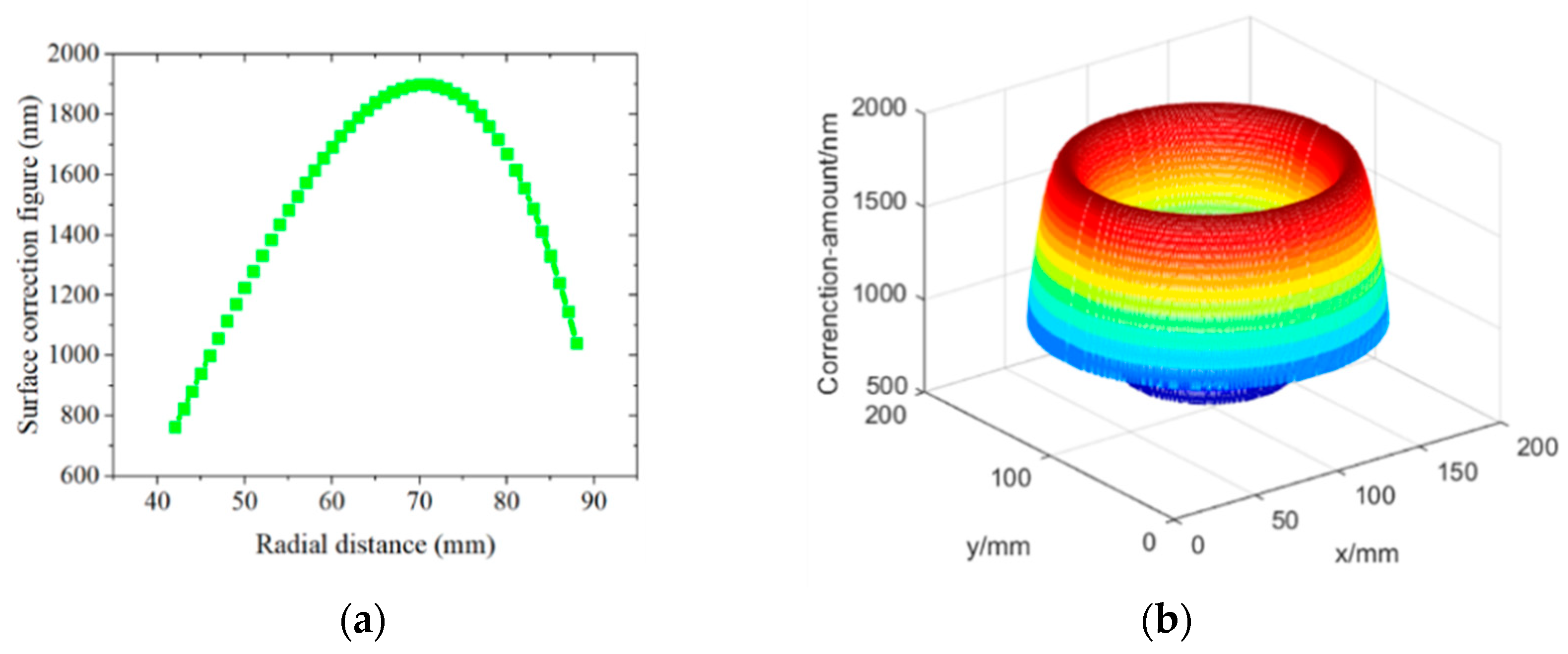
As the hyperboloid surface in this study was rotationally symmetric, the best-fit sphere was calculated using the profile of the hyperboloid in the radial direction. Figure 2a shows the difference between the best-fit spheres before and after optimization of the fitting method. As a result, the surface correction figures calculated by two methods are shown in Figure 2b. The size of the area under the curve demonstrates the advantage of optimization. Figure 3 shows the surface correction figure within the effective aperture (R = 42–88 mm) and the corresponding correction-amount distribution on the surface, respectively.

3. Method

Considering that the correction-amount distribution has rotational symmetry, an experiment was carried out using a direct current (DC) magnetron sputtering coating system with substrate planetary motion developed in our laboratory. [19]. Herein, profile-coating with an irregular mask that also has rotational symmetry to control the film thickness distribution is a reliable method for fabricating the mirror. In the following three subsections, the planetary motion magnetron sputtering coating system is presented, followed by details of principles of the profile-coating method and the design of the mask.

3.1. Planetary Motion Magnetron Sputtering Coating System

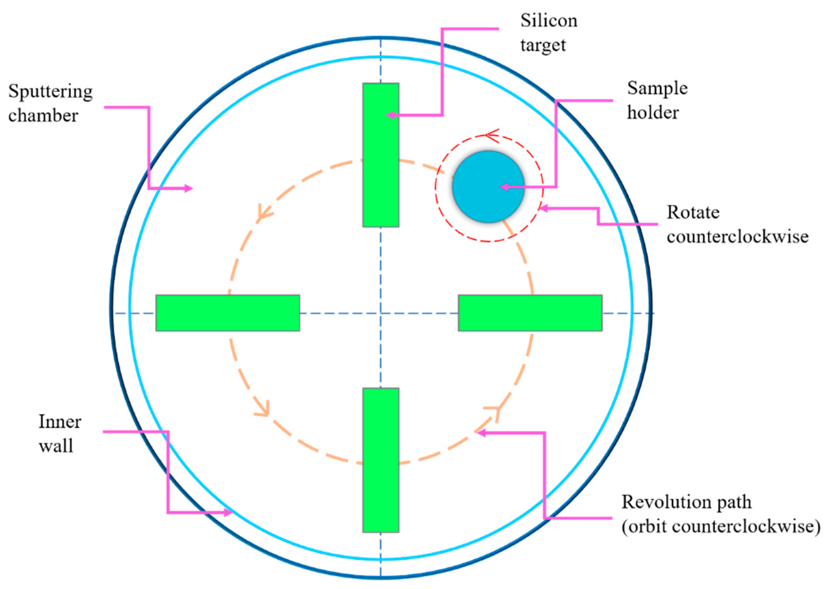
The experiment was carried out using a magnetron sputtering coating system with substrate planetary motion in this study. The use of such equipment is beneficial to avoid film thickness errors on the same circumference when the spherical surface is corrected to the rotational symmetric hyperboloid surface. As shown schematically in Figure 4, there are four rectangular magnetron sputtering targets, evenly distributed in the circular vacuum chamber and installed vertically upwards. Each target is equipped with a shielding sleeve to prevent mutual contamination between different sputtering materials during the coating process. The sample holder is placed vertically above the target and revolves around the main axis of the vacuum chamber. Meanwhile, the high-speed rotation function of the sample holder ensures the uniformity of the film deposited on the surface of the sample holder.

3.2. Principles of Profile-Coating Method

The traditional process of the profile-coating method utilizes a contoured aperture mask in a DC magnetron sputtering system with a simple linear motion of the substrates to coat the design profile [13]. An irregular shape mask is equipped between the substrate and the target for coating. A mask with a contour designed through mathematical calculations is placed between the substrate and the target in order to obtain the desired film thickness distribution at different positions, as shown in Figure 1a. Generally, the mask is very close to the substrate to prevent an oblique incidence of the target particles and the power of the target gun remains constant. In this study, a uniform linear motion of the substrates was replaced with a uniform circular motion based on the planetary motion magnetron sputtering coating system. A designed mask was installed 5 mm below the sample in order to allow a specific number of sputtered particles to be deposited on a specific area of the sample. In this way, the desired irregularly shaped surface could be obtained. In general, the revolution process controlled the number of particles reaching the sample; the mask controlled the number of deposited particles at each position of the sample and the rotation process controlled the uniformity of the film at the same radius of the sample.

3.3. Mask Design

In the planetary motion magnetron sputtering coating system, the sample holder rotates at a high speed and the center of rotation is concentric with the center of the sample holder, ensuring a uniform thickness of the film deposited on the same circumference of the substrate. Thus, the key to the fabrication of the rotational symmetric hyperboloid surface is to control the film thickness distribution at different circumferences, which is achieved by an irregular mask.
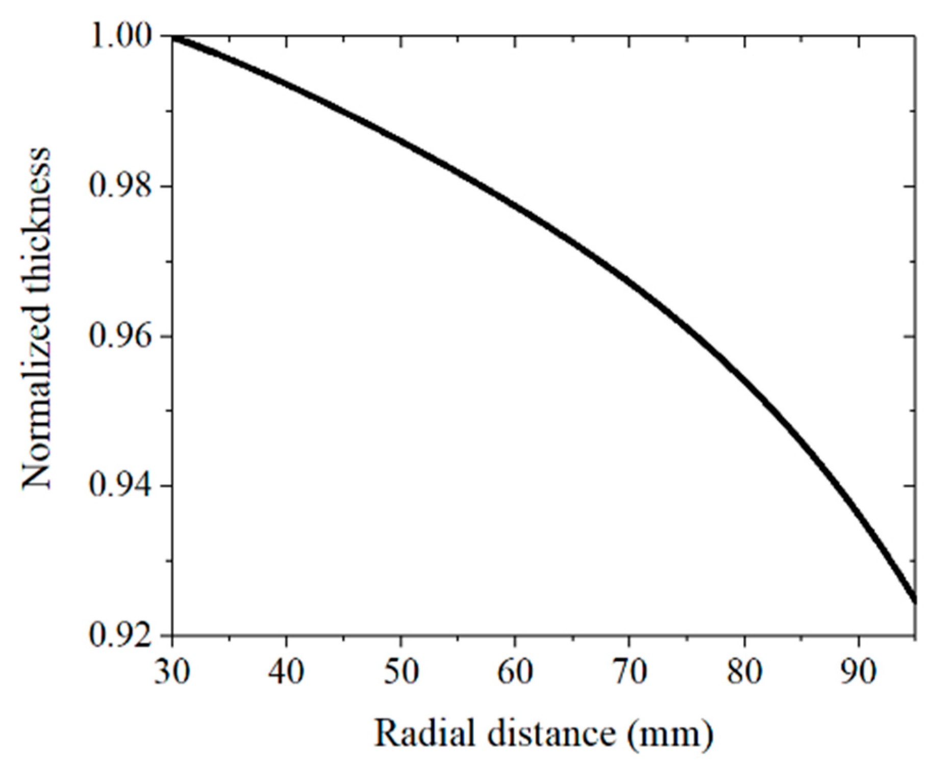
Before designing the mask, it is necessary to know the deposition distribution of the film on the sample holder without the mask. Due to the silicon film with a thickness of 2000 nm still having the advantages of low stress, better stability and less roughness [20], in this study, we chose it as the material for profile coating. The deposition conditions are shown in Table 1. According to the previous experimental results in the laboratory, the radial film deposition distribution shown in Figure 5 can be obtained.
The design principle of the mask is to vary the thickness of the film deposited on the substrate at different radii by partially shielding circles corresponding to different radii. The ratio of the opening angle is calculated based on the desired film distribution.
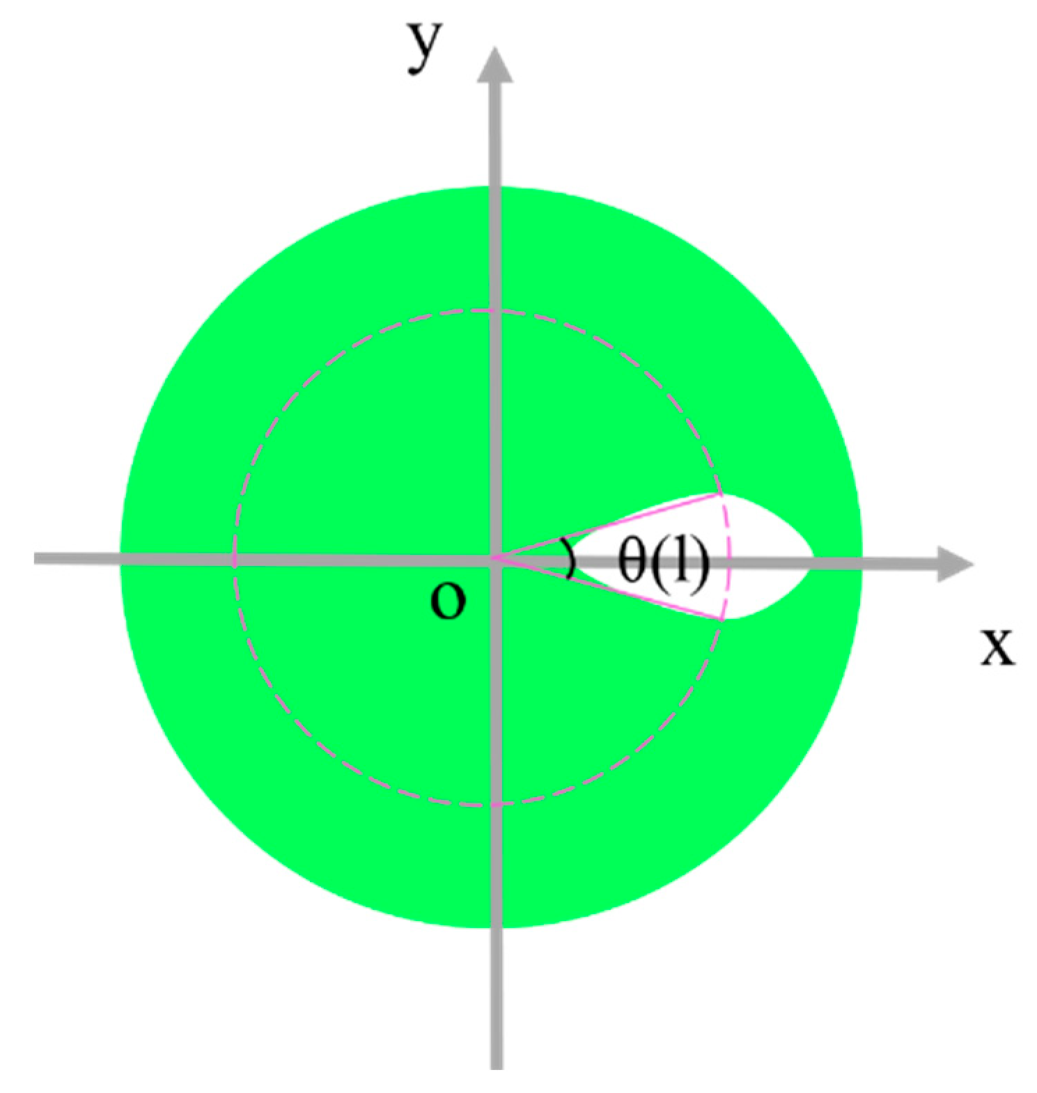
A rectangular coordinate system in which the origin is the center o of the mask is built as shown in Figure 6. The opening angle at radius l on the mask is θ l , which can be expressed as:
θ l = 360 ° × h l H l a l
where Hl is the film thickness of the unobstructed part of the sample, hl is the desired film thickness on the sample. al is the normalized value of radial film thickness distribution.
It should be noted that Hl can be set to any value greater than the maximum correction amount. Here, we set the value of Hl corresponding to the maximum opening angle of 171° to 4000 nm in consideration of the processing difficulty.
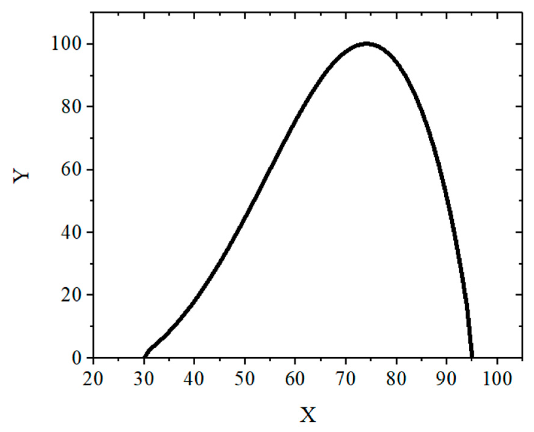
Then, the opening angle can be further converted into the coordinates of each position on the mask to facilitate fabrication. The opening area is equally divided into two symmetrical parts, and the corresponding center angle of each part is half of the total opening angle. In this way, the position coordinates of the edge of the opening angle at the radius of 30–95 mm of the mask are shown in Figure 7. The expression for this is:
{ x = l × cos   ( θ l 2 ) y = l × sin   ( θ l 2 )
where l is the radius corresponding to different circles, and θ l is the opening angle on different circumferences.
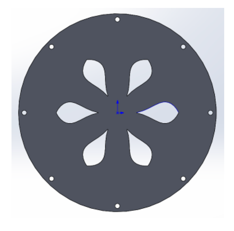
In actual mask fabrication, we generally use a multi-aperture mask to replace the single-aperture mask in Figure 6 to make the profile of the opening edge smoother, thereby reducing film thickness errors. However, considering the processing error of the mask, if the opening area is divided into too many parts, this will also cause error accumulation. Moreover, comprehensively considering the correction size and correction accuracy, as shown in Figure 8, we use six opening areas of the same size on the mask in order to reduce the film thickness error. Although the low hollow rate of the mask will reduce the deposition rate, it will make the structure of the mask more stable and relatively improve the manufacturing accuracy.

4. Experiment

4.1. Film Thickness Calibration

After obtaining the mask, it is important to calibrate the film thickness in the radial direction of the substrate due to the processing error of the mask. At present, X-ray Reflection (XRR) and Transmission Electron Microscopy (TEM) are the regular methods for measuring film thickness. However, the XRR test is inapplicable for analyzing film thicknesses of hundreds of nanometers [21,22]. Although TEM can guarantee certain accuracy, it is expensive and not suitable for large-area measurements [23]. Here, we proposed a step test combined with an optical profiler to solve this problem.
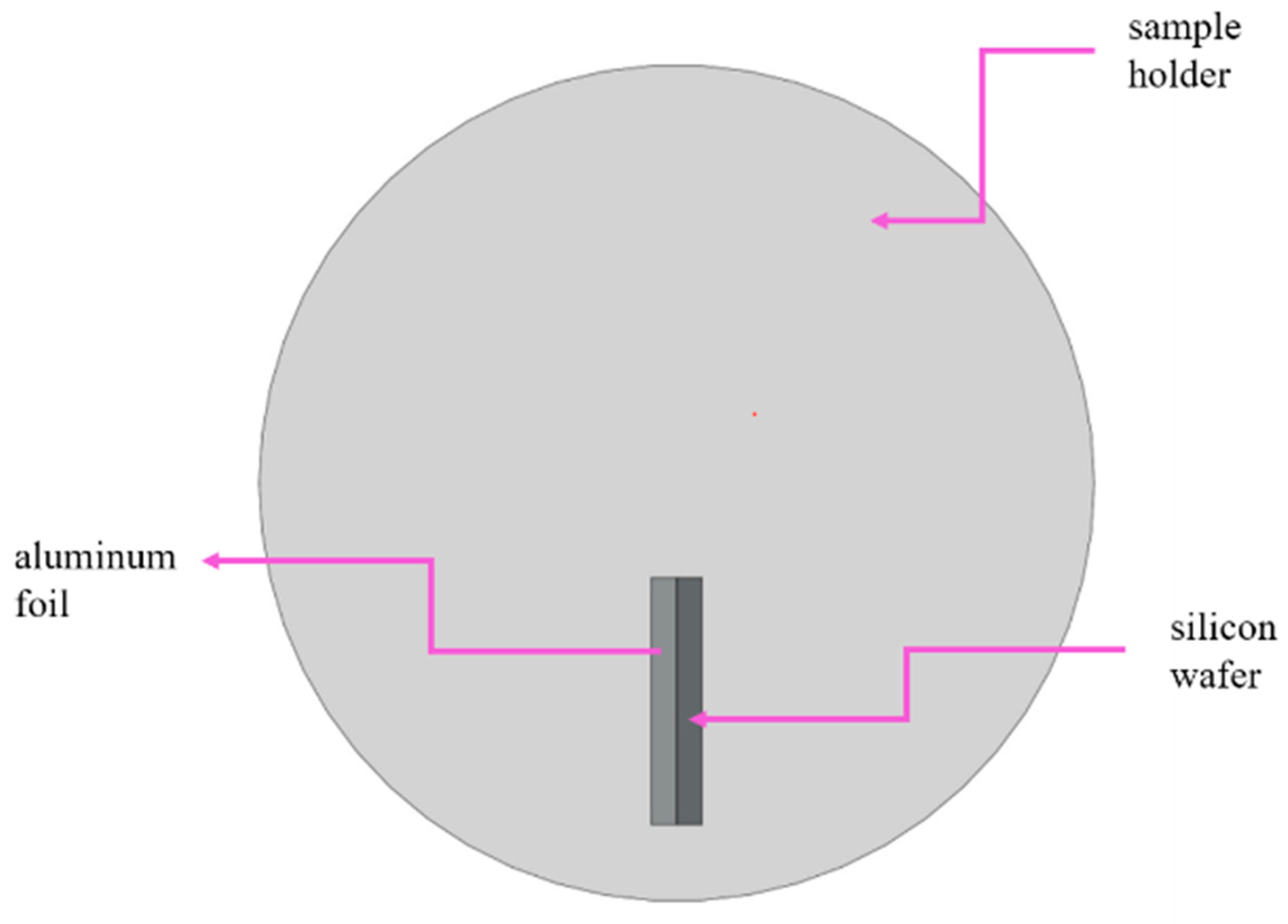
We first deposited a film on a silicon wafer under deposition conditions consistent with Table 1. In order to facilitate subsequent step tests, a 0.1 mm aluminum foil was used to cover the other half of the silicon wafer. Then, a stepped film in the radial direction of the substrate was obtained on the silicon wafer. The specific placement is shown in Figure 9. Furthermore, for the purpose of attaining better uniformity of the film thickness on the same circumference of the substrate, the sample holder rotated at a rate of 100 r/min. Meanwhile, based on the design of the mask and the deposition rate of the film without the mask, the sample holder also revolved around the center of the chamber for 48 revolutions at a constant speed of 0.018 r/s to achieve the desired film thickness distribution.
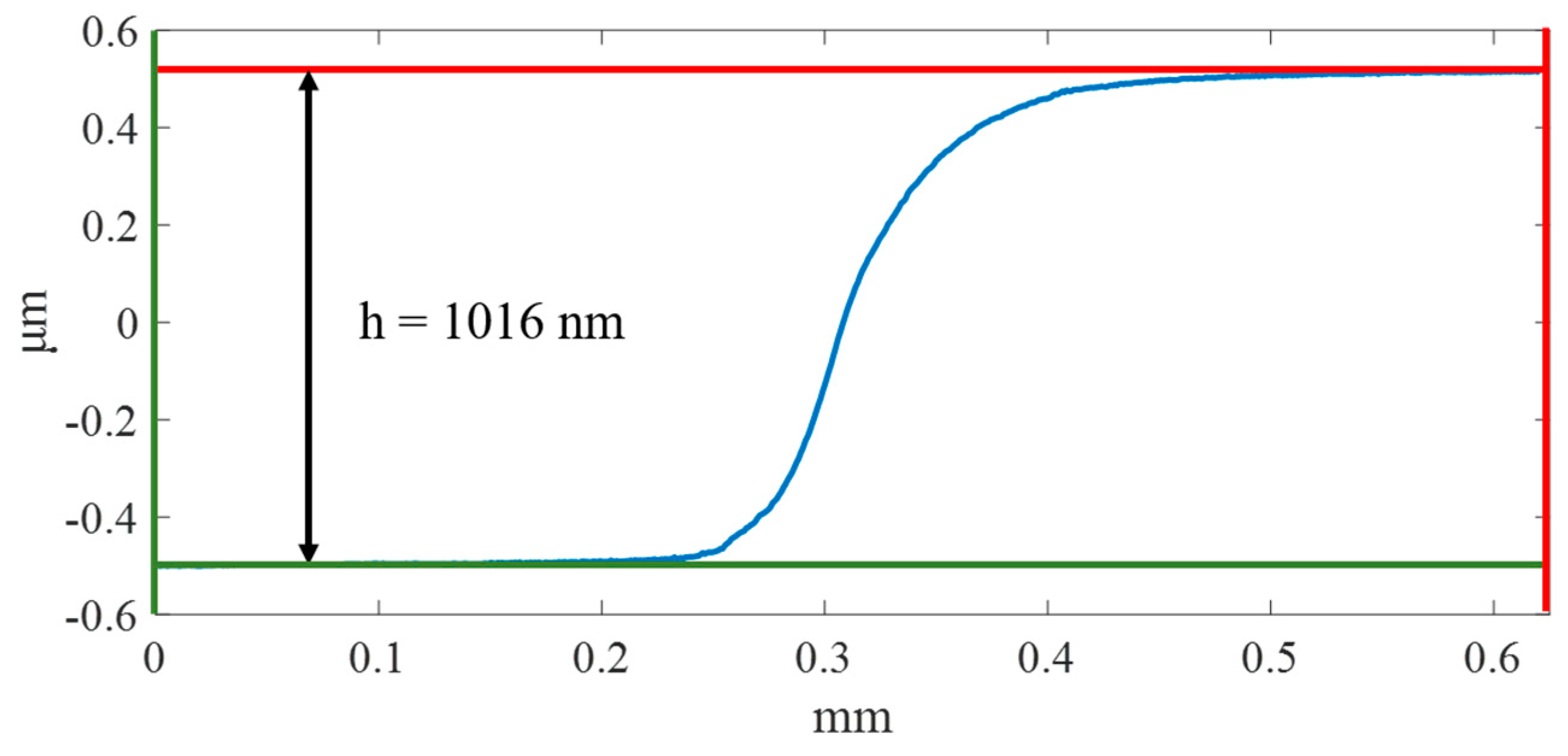
To quantitatively evaluate the film thickness distribution, the surface of the step edge in the radial direction of the substrate was measured using an optical profiler (Contour GT-X3, Bruker, Billerica, MA, USA). A 10× lens was used to obtain a surface topography of an aperture of 0.6 mm × 0.469 mm every 1 mm in the direction of the step edge (Figure 10). To achieve high accuracy during measurements, 30 image frames were captured and averaged at each test point (Figure 11a). Subsequently, the film thickness distribution was achieved by calculating the height difference between the coated area and the uncoated area in each image with a repeatability error typically less than 1 nm (Figure 11b), meeting the requirement of measurement accuracy of less than 5 nm.
However, the lens angle of the optical profiler was not always completely perpendicular to the sample surface in actual measurements. This caused the uncoated area to show a slope (Figure 12), thereby the height difference between the two ends of the interception was inaccurate.
Thus, the question of how to confirm the degree of tilt is critical. Since the surface of the wafer used was ultra-smooth, the height profile of the surface was very flat in the area without any film coating. When the film was coated, the surface height fluctuations increased significantly because of rapid changes in surface height. It can be clearly seen in Figure 13b that the first derivative of the step height starts to change abruptly at x = 0.15 mm. Therefore, the uncoated area (the area to the left of the orange vertical line) can be confirmed. A straight line was used to fit the curve of the uncoated area to correct the height difference that comes from the tilt error as shown in Figure 13c. The actual height difference of this position was calculated to be 992 nm, which was 24 nm different from the 1016 nm obtained via direct measurement, improving the accuracy of test results.
Test results of the coating area from 42 mm to 88 mm in the radial direction after the tilt-correction process are shown in Figure 14. The actual film thickness in the radial direction is different from the desired film thickness. The maximum film thickness error is 105 nm and the figure error is 38.9 nm RMS, which comes from the processing error of the mask. Although the processing accuracy of the mask can reach 0.05 mm currently, the film thickness error will accumulate rapidly when the film thickness reaches the micron scale, resulting in the actual surface topography being inconsistent with the theoretical surface topography.
Therefore, manual trimming of the mask is necessary. It is a reasonable calculation method to calculate the thickness error to modify the opening size of the mask accordingly. The specific trimming method can be expressed as:
θ gl = h gl h fl θ fl
where h gl and h fl represent the target thickness and actual thickness of each point, respectively. Correspondingly, θ gl and θ fl represent the corrected angle and current angle of the open area on the mask, respectively.
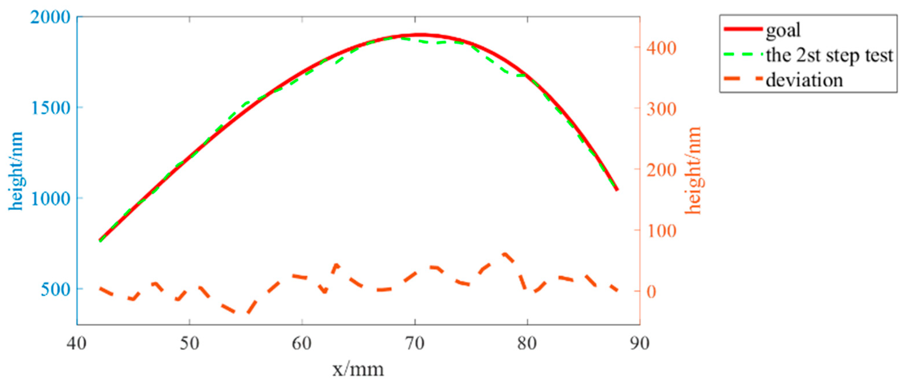
Under the same experimental conditions as before, the second film thickness calibration experiment was carried out with the trimmed mask. The step height profile was found to be closer to the target profile than the first calibration result. The film thickness distribution test results are shown in Figure 15, with a thickness error of less than 62 nm. Compared with the first film thickness calibration, the maximum film thickness error was reduced by 43 nm, and the figure error was 21.2 nm RMS, reduced by 17.7 nm RMS.
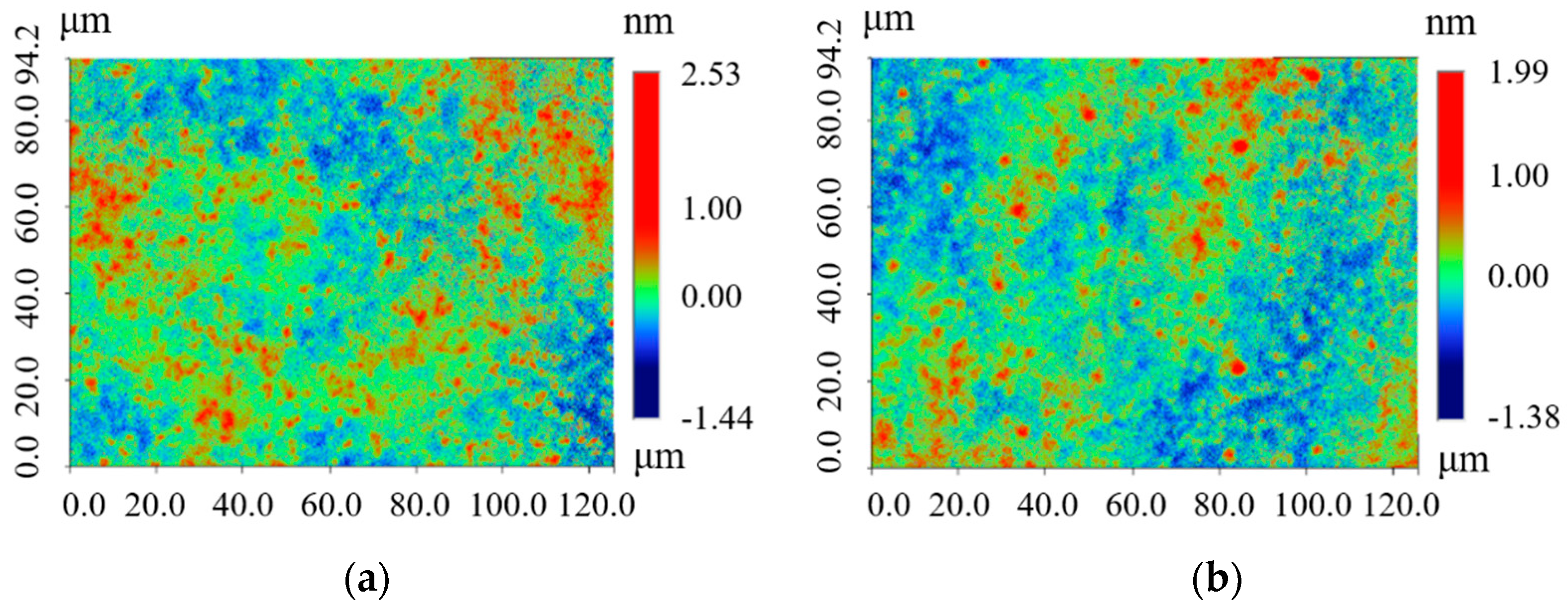
In addition, to study the roughness change after coating, a zerodur substrate was used to deposit silicon film at a depth of 2000 nm. The roughness values of the surface before and after coating based on the data obtained using the optical profiler (50×) are shown in Figure 16. It was found that the surface roughness values before and after the experiment were 0.308 and 0.334 nm RMS, respectively. Therefore, the surface roughness does not change significantly after coating.

4.2. Spherical Mirror Coating

The substrate of the finished product was a spherical zerodur mirror with a diameter of 180 mm and a low thermal expansion coefficient. The deposition conditions were still consistent with Table 1.
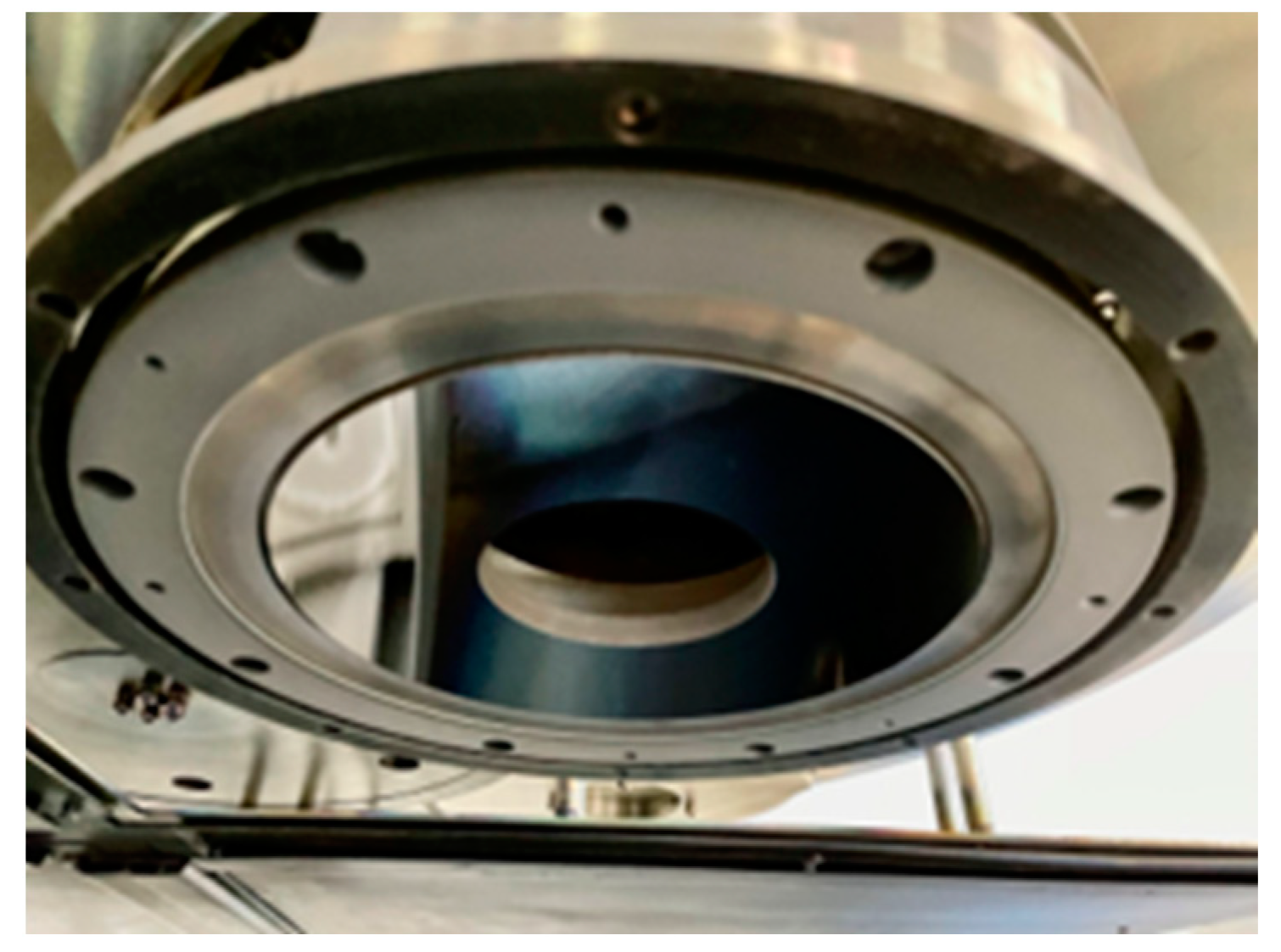
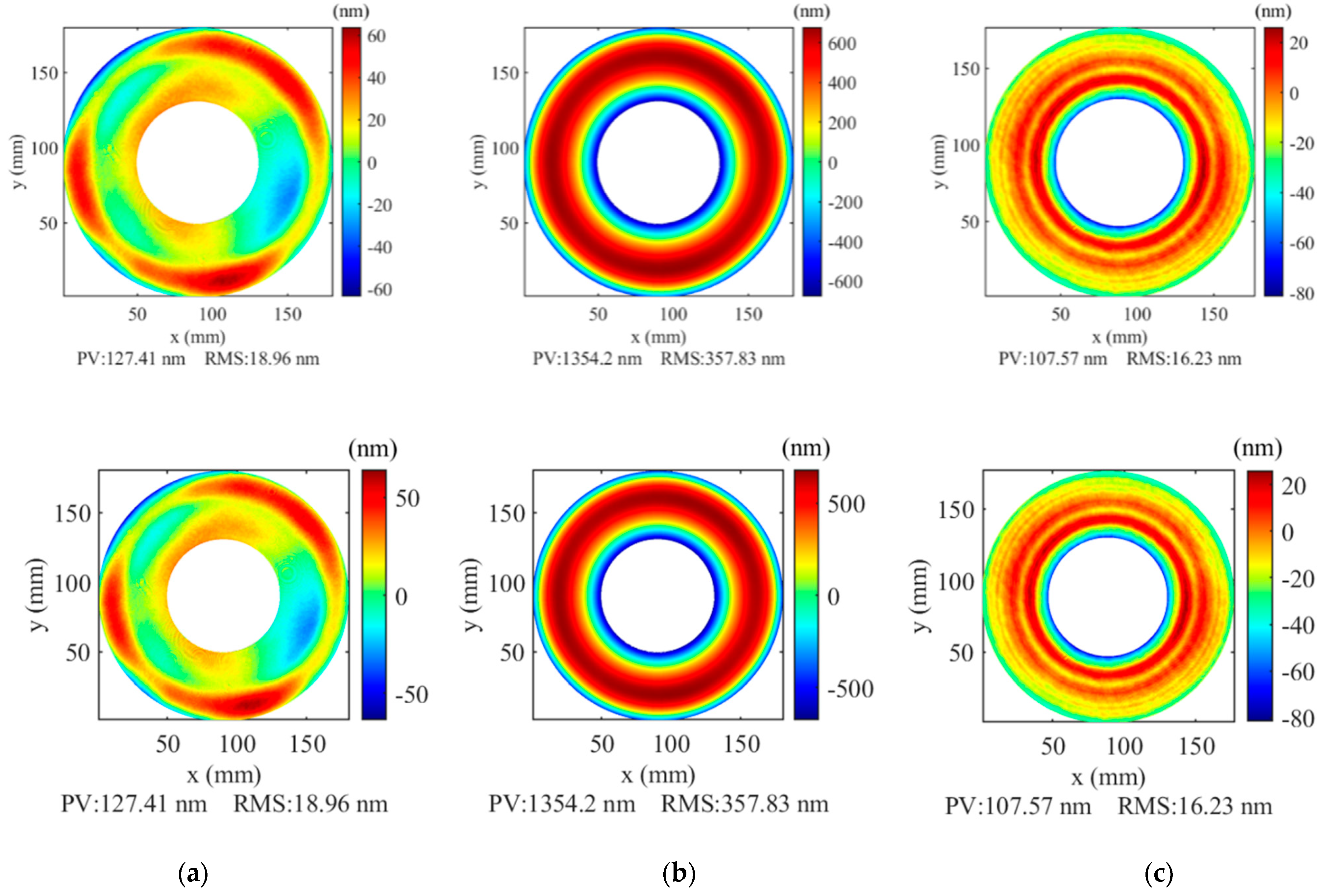
Finally, the surface of the mirror was coated with a silicon film, as shown in Figure 17. The surface was characterized using a Zygo (DynaFiz TM) interferometer. The test mode chosen is PSI (Phase-Shifting Interferometry) mode with 1200 × 1200 pixels. The reference mirror diameter is 100 mm. Repeatability error is typically 1.5 nm RMS. Thirty image frames were captured and averaged to improve measurement accuracy. Since the deviation between the hyperboloid and the sphere is relatively small and within the measurement range of the interferometer, it can be considered as the difference between the two surfaces. The measurement results revealed a significant change in the rotational symmetry of the surface topography. Figure 18a,b shows the surface topography of the spherical mirror before and after coating. Compared with the correction-amount distribution in Figure 2b, the residual surface error of 42–88 mm in the radial direction was 16.23 nm RMS without the initial surface error of the spherical mirror, as shown in Figure 18c.
Moreover, in order to reflect the actual film thickness distribution intuitively, 360 radius profiles of the coated surface (in which each radius is 1 degree apart), obtained by subtracting the initial surface after coating, were extracted and compared with the target profile, as shown in Figure 19. The figure shows the comparison of the film thickness distribution between the target surface correction figure, the second film thickness calibration experiment and the finished product experiment. The x value is the position of the coating area on the radius of the spherical mirror. As the value of x increases, the film thickness distribution follows a trend that first increases and then decreases. Whether it is a film thickness calibration experiment or a finished product experiment, the film profile is very similar to the target surface correction figure, demonstrating that the process is successful.
In contrast with the calibration experiment, the film thickness on the spherical mirror shows a downward trend on both sides of the coating area. There are generally two factors accounting for this phenomenon. First, the assembly error of the mask per experiment will reduce the repeatability of the experiment. Second, there is compressive stress caused by the thickness of the silicon film [24,25,26]. Since the thickness of the silicon film varies at different radii of the substrate, the film growth rate in each region is different. Furthermore, the back of the substrate is light-weighted, so this experiment did not focus on the stress of the silicon film.

5. Conclusions

In this paper, we proposed an effective method for rotational symmetric aspheric surface correction by magnetron sputtering. First, an irregularly-shaped mask was calculated and made to achieve the desired film thickness distribution on the substrate, based on the planetary motion magnetron sputtering coating system to perform rotational symmetry coating. Second, film thickness calibration was carried out to reduce the effect of the processing error of the mask as the correction amount reaches the micron scale. It is observed that the figure error was reduced from 38.9 nm RMS to 21.2 nm RMS after trimming the mask according to the calibration results. Last, the efficiency of film thickness calibration has been verified on the correction of the rotational symmetric hyperboloid surface by applying the trimmed mask. The film thickness error at the effective radius of 42–88 mm was brought down to 16.23 nm RMS, which proves the prospects of this form of profile coating technology.

Author Contributions

Conceptualization, experiment, formal analysis, and writing—original draft, H.H.; XRR testing and analysis, Y.F.; funding acquisition, supervision, and project administration, J.Y. and R.Q.; reviewing, and editing, Z.W. All authors have read and agreed to the published version of the manuscript.

Funding

This research was funded by National Natural Science Foundation of China (12003016, 62105244), Strategic Priority Research Program of the Chinese Academy of Sciences (Grant No. XDA15018400).

Institutional Review Board Statement

Not applicable.

Informed Consent Statement

Not applicable.

Data Availability Statement

The data presented in this study are available on request from the corresponding author.

Conflicts of Interest

The authors declare no conflict of interest.

References

  1. Heynacher, E. Aspheric optics. How they are made and why they are needed. Phys. Technol. 1979, 10, 124. [Google Scholar] [CrossRef]
  2. Linfoot, E. On some optical systems employing aspherical surfaces. Mon. Not. R. Astron. Soc. 1943, 103, 210–221. [Google Scholar] [CrossRef] [Green Version]
  3. Sharma, R.; Mishra, V.; Khatri, N.; Garg, H.; Karar, V. A hybrid fabrication approach and profile error compensation for silicon aspheric optics. Proc. Inst. Mech. Eng. Part B J. Eng. Manuf. 2017, 233, 1600–1607. [Google Scholar] [CrossRef]
  4. Wynne, C.G. Ritchey-Chretien telescopes and extended field systems. Astrophys. J. 1968, 152, 675. [Google Scholar] [CrossRef]
  5. Wetherell, W.B.; Rimmer, M.P. General analysis of aplanatic Cassegrain, Gregorian, and Schwarzschild telescopes. Appl. Opt. 1972, 11, 2817–2832. [Google Scholar] [CrossRef]
  6. Aspden, R.; McDonough, R.; Nitchie, F.R. Computer assisted optical surfacing. Appl. Opt. 1972, 11, 2739–2747. [Google Scholar] [CrossRef]
  7. Jones, R.A. Optimization of computer controlled polishing. Appl. Opt. 1977, 16, 218–224. [Google Scholar] [CrossRef]
  8. Jones, R.A. Fabrication using the computer controlled polisher. Appl. Opt. 1978, 17, 1889–1892. [Google Scholar] [CrossRef]
  9. Allen, L.N.; Keim, R.E.; Lewis, T.S.; Ullom, J.R. Surface error correction of a Keck 10-m telescope primary mirror segment by ion figuring. Proc. SPIE 1991, 1531, 195–204. [Google Scholar]
  10. Jacobs, S.D.; Golini, D.; Hsu, Y.; Puchebner, B.E.; Strafford, D.; Prokhorov, I.V.; Fess, E.M.; Pietrowski, D.; Kordonski, W.I. Magnetorheological finishing: A deterministic process for optics manufacturing. Proc. SPIE 1995, 2576, 372–382. [Google Scholar]
  11. Yamauchi, K.; Mimura, H.; Inagaki, K.; Mori, Y. Figuring with subnanometer-level accuracy by numerically controlled elastic emission machining. Rev. Sci. Instrum. 2002, 73, 4028–4033. [Google Scholar] [CrossRef]
  12. Ice, G.E.; Chung, J.S.; Tischler, J.Z.; Lunt, A.; Assoufid, L. Elliptical X-ray microprobe mirrors by differential deposition. Rev. Sci. Instrum. 2000, 71, 2635–2639. [Google Scholar] [CrossRef]
  13. Liu, C.; Assoufid, L.; Macrander, A.T.; Ice, G.E.; Tischler, J.Z. Profile coating for KB mirror applications at the Advanced Photon Source. Proc. SPIE 2002, 4782, 104–112. [Google Scholar]
  14. Liu, C. Profile coating and its application for Kirkpatrick-Baez mirrors. Opt. Eng. 2003, 42, 3622–3628. [Google Scholar] [CrossRef]
  15. NTRS-NASA Technical Reports Server. Available online: https://ntrs.nasa.gov/citations/20120002986 (accessed on 27 October 2020).
  16. Kilaru, K.; Atkins, C.; Ramsey, B.D.; Kolodziejczak, J.K.; Lis, T.M.; Gubarev, M.V.; O’Dell, S.L.; Gaskin, J.A.; Broadway, D.M. Progress in differential deposition for improving the figures of full-shell astronomical grazing incidence X-ray optics. In Optics for Euv, X-ray, and Gamma-Ray Astronomy Vii; SPIE: Bellingham, WA, USA, 2015; Volume 9603, p. 96031F. [Google Scholar]
  17. Morawe, C.; Bras, P.; Labouré, S.; Perrin, F.; Vivo, A. Mirror figure correction on variable length scales. Int. Soc. Opt. Photonics 2021, 11837, 118370C. [Google Scholar]
  18. Kim, J.; Kim, J.S.; Kim, H.Y.; Ryu, C.K.; Jeong, D.; Chae, B.; Lim, J.; Kim, J.H.; Rah, S. Development of a one-dimensional differential deposition system for X-ray mirror figure correction. Precis Eng. 2021, 71, 1–6. [Google Scholar] [CrossRef]
  19. Huang, H.; Jiang, L.; Yao, Y.; Zhang, Z.; Wang, Z.; Qi, R. Controlling Film Thickness Distribution by Magnetron Sputtering with Rotation and Revolution. Coatings 2021, 11, 599. [Google Scholar] [CrossRef]
  20. Shi, Y.; Qi, R.; Feng, Y.; Huang, Q.; Shen, Z.; Wang, Z. Microstructure, roughness, and stress properties of silicon coatings for shape correction of Kirkpatrick–Baez mirrors. Opt. Eng. 2019, 58, 015103. [Google Scholar] [CrossRef]
  21. Benediktovitch, A.; Feranchuk, I.; Ulyanenkov, A. X-ray Reflectivity. In Theoretical Concepts of X-ray Nanoscale Analysis; Springer: Berlin/Heidelberg, Germany, 2014; pp. 71–118. [Google Scholar]
  22. Wormington, M.; Panaccione, C.; Matney, K.M.; Bowen, D.K. Characterization of structures from X-ray scattering data using genetic algorithms. Philosophical Transactions of the Royal Society of London Series A: Mathematical. Phys. Eng. Sci. 1999, 357, 2827–2848. [Google Scholar] [CrossRef]
  23. Reimer, L. Transmission Electron Microscopy: Physics of Image Formation and Microanalysis; Springer: Berlin/Heidelberg, Germany, 2013. [Google Scholar]
  24. Freund, L.B.; Suresh, S. Thin Film Materials: Stress, Defect Formation and Surface Evolution; Cambridge University Press: Cambridge, UK, 2004. [Google Scholar]
  25. Nadimpalli, S.P.; Sethuraman, V.A.; Bucci, G.; Srinivasan, V.; Bower, A.F.; Guduru, P.R. On plastic deformation and fracture in Si films during electrochemical lithiation/delithiation cycling. J. Electrochem. Soc. 2013, 160, A1885. [Google Scholar] [CrossRef] [Green Version]
  26. Yu, B.; Jin, C.; Yao, S.; Li, C.; Liu, Y.; Zhou, F.; Guo, B.; Wang, H.; Xie, Y.; Wang, L. Low-stress and high-reflectance Mo/Si multilayers for extreme ultraviolet lithography by magnetron sputtering deposition with bias assistance. Appl. Opt. 2017, 56, 7462–7468. [Google Scholar] [CrossRef] [PubMed]
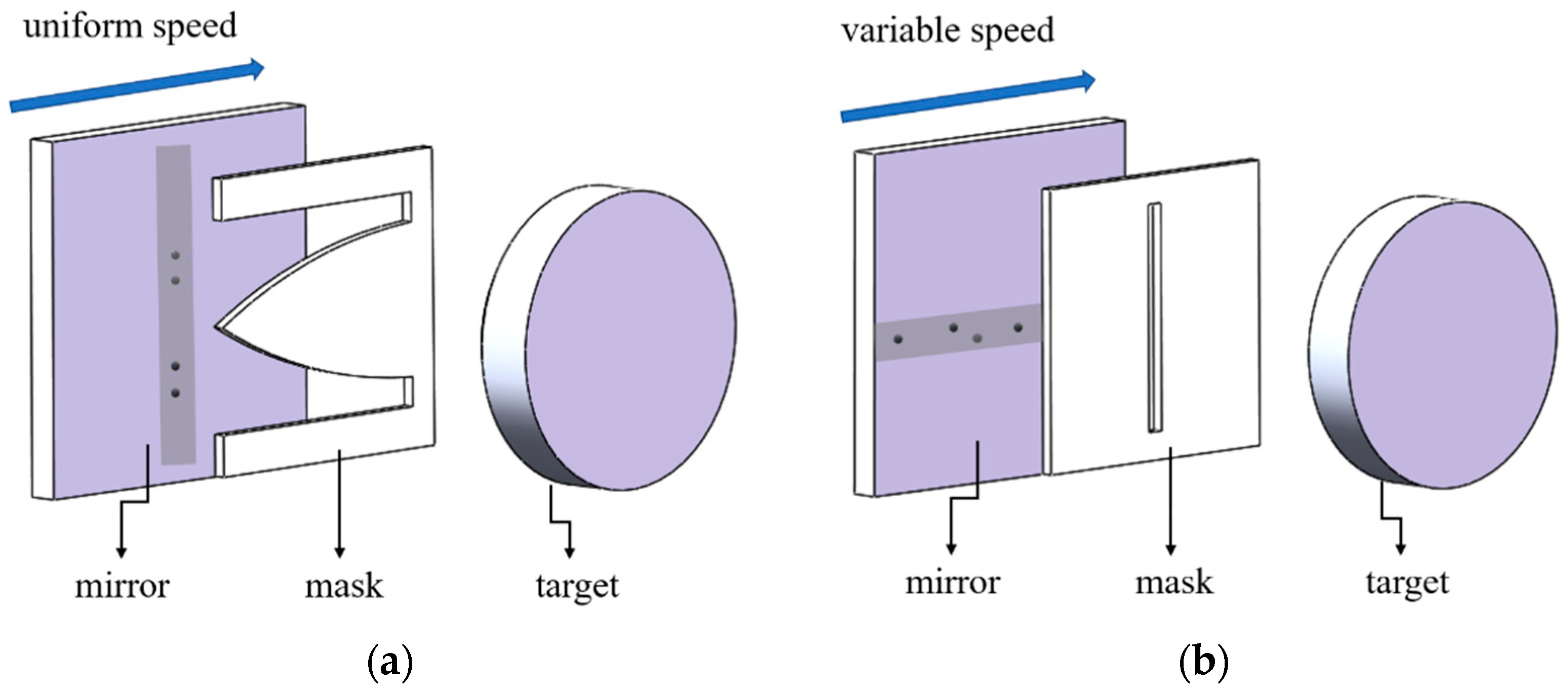
Figure 1. Mask-assisted magnetron sputtering: (a) profile-coating, (b) differential-deposition.
Coatings 12 01055 g001
Figure 2. Effectiveness of the optimization fitting method. (a) best-fit sphere; (b) surface correction figure.
Coatings 12 01055 g002
Figure 3. (a) The surface correction figure (R = 42–88 mm); (b) the correction-amount distribution.
Coatings 12 01055 g003
Figure 4. Planetary motion magnetron sputtering coating system.
Coatings 12 01055 g004
Figure 5. The radial film deposition distribution.
Coatings 12 01055 g005
Figure 6. Schematic diagram of the calculation of the mask design opening ratio.
Coatings 12 01055 g006
Figure 7. The position coordinates of the edge of the opening angle on the mask.
Coatings 12 01055 g007
Figure 8. Mask design.
Coatings 12 01055 g008
Figure 9. Step shielding mode.
Coatings 12 01055 g009
Figure 10. Single point test result.
Coatings 12 01055 g010
Figure 11. Single−point test result: (a) step topography, (b) step height profile (red horizontal line: the coated area, green horizontal line: the uncoated area, blue line: step height profile).
Coatings 12 01055 g011
Figure 12. Height−error due to tilt (red horizontal line: the coated area, green horizontal line: the uncoated area, blue line: step height profile).
Coatings 12 01055 g012
Figure 13. Tilt−correction process: (a) step height profile, (b) first-order derivative height, (c) corrected step height profile.
Coatings 12 01055 g013
Figure 14. Comparison of film thickness distribution with ideal thickness distribution.
Coatings 12 01055 g014
Figure 15. Comparison of the second film thickness distribution with the ideal thickness distribution.
Coatings 12 01055 g015
Figure 16. Surface roughness: (a) before coating, (b) after coating.
Coatings 12 01055 g016
Figure 17. The mirror in the chamber.
Coatings 12 01055 g017
Figure 18. (a) The surface topography before coating; (b) the surface topography after coating; (c) the fabrication error.
Coatings 12 01055 g018
Figure 19. Radial film thickness distribution.
Coatings 12 01055 g019
Table 1. Deposition conditions.
Background PressureWorking GasWorking PressureTarget MaterialSputtering PowerTarget–Substrate Distance
1.5 × 10⁶ Torr99.999% Ar1 mTorrSi300 W115 mm
Publisher’s Note: MDPI stays neutral with regard to jurisdictional claims in published maps and institutional affiliations.