Communication

THz Surface Plasmons in Wide and Freestanding Graphene Nanoribbon Arrays

by
Talia Tene
1,
Marco Guevara
2,
Yesenia Cevallos
3,
Miguel Ángel Sáez Paguay
4,
Stefano Bellucci
5 and
Cristian Vacacela Gomez
6,*
1
Department of Chemistry, Universidad Técnica Particular de Loja, Loja 110160, Ecuador
2
Faculty of Mechanical Engineering, Escuela Superior Politécnica de Chimborazo (ESPOCH), Riobamba 060155, Ecuador
3
College of Engineering, Universidad Nacional de Chimborazo, Riobamba 060108, Ecuador
4
Facultad de Recursos Naturales, Escuela Superior Politécnica de Chimborazo (ESPOCH), Orellana 220201, Ecuador
5
INFN-Laboratori Nazionali di Frascati, I-00044 Frascati, RM, Italy
6
UNICARIBE Research Center, University of Calabria, I-87036 Rende, CS, Italy
*
Author to whom correspondence should be addressed.
Coatings 2023, 13(1), 28; https://doi.org/10.3390/coatings13010028
Submission received: 18 November 2022 / Revised: 8 December 2022 / Accepted: 20 December 2022 / Published: 23 December 2022
(This article belongs to the Special Issue 2D Materials-Based Thin Films and Coatings)

Abstract

:
Graphene is a thin-film carbon material that has immense potential as a key ingredient in new nanoelectronic and nanophotonic devices due to its unique characteristics. In particular, plasmons in graphene appear as a practical tool for the manipulation of light with potential applications from cancer treatment to solar cells. A motivating tunability of graphene properties has been observed in graphene nanoribbons (GNRs) due to their geometrically controllable bandgaps that, in turn, influence the plasmonic properties. The formidable effort made over recent years in developing GNR-based technologies is, however, weakened by a lack of predictive approaches that draw upon available semi-analytical electromagnetic models. An example of such a framework is used here, focusing on experimentally realized GNRs from 155 to 480 nm wide and organized as two-dimensional (2D) GNR arrays. The results show that the plasmon frequency behavior is highly affected by the experimental setup or geometrical factors. In particular, the bandgap of the analyzed systems is of the order of a few meV with a density of states opening around zero energy (Fermi level) in contrast to what is observed in graphene. From the plasmonic part, it is observed in all 2D GNR arrays that the frequency–momentum trend follows a q -like plasmon dispersion whose plasmon frequency can be increased substantially by increasing the ribbon width or charge density concentration. Forbidden plasmon regions are observed for high values of plasmon excitation angle or electron relaxation rate. From a sensing point of view, the important finding is the fact that 2D GNR arrays of 155 nm wide with high values of electron relaxation rate have plasmon responses similar to those observed for α thrombin in water. Our predictions are projected to be of fast support for detecting plasmons in more complex designs of ribbon nanodevices with potential applications in molecular sensing of aqueous molecules.

1. Introduction

Surface plasmons (SPs) are so-called collective excitations of valence electrons in conducting or semiconducting materials [1]. They have been explored in many applications such as integrated nanophotonics [2], sensing [3], metasurfaces [4], and photovoltaics [5]. In particular, SPs have been realized at the surface of noble metals (e.g., gold or silver), finding their resonance modes mostly in the visible part of the electromagnetic spectrum [6]. However, these collective oscillations in metals show a lack of tunability of the plasmon frequency as well as a small plasmon propagation length [7]. Alternatively, SPs in graphene show various rewards compared to metals, mainly: (i) these oscillations are found in the terahertz-to-midinfrared frequency range with potential applications in sensing and communications [8], and (ii) SPs in graphene have much stronger confinement and large tunability [9]. Nevertheless, the electron scattering observed in supported graphene significantly degrades the plasmon propagation length.
To address this problem, it has been proposed to change the system dimensionality from two-dimensional (2D) graphene to quasi-one-dimensional (1D) graphene so-called graphene nanoribbons (GNRs). This approach makes it possible to substantially reduce the plasmon damping and improve the plasmon propagation length [10]. Graphene, a 2D thin film made of carbons and arranged in a honeycomb framework, has already demonstrated excellent physical, chemical, and mechanical properties [11] that guarantee interesting applications pursued by academia and industry [12]. While graphene displays great promise for future electronics and photonics, the major limitation is its lack of a bandgap. In this context, thin strips of graphene, i.e., GNRs, have evidenced superior electronic, optical, and magnetic properties [13] that emerge from the structural boundary conditions imposed by the ribbon width, crystallographic symmetry, and chiral edges [14]. GNR systems, particularly, have arisen as promising candidates for introducing bandgaps (from a few meV to eV) that are inversely proportional to ribbon width [15]. GNRs have mostly been studied for applications such as resonators [16] and field-effect transistors [17].
Nowadays, SPs in GNRs have been realized and predicted to exist [18,19]; however, in order to minimize electron scattering and obtain the best possible electronic and plasmonic properties, it is necessary to look at GNRs organized as 2D periodic arrays [20]. Such structures have been realized by Fei et al., with GNRs from 155 to 480 nm wide [21], where two plasmons were observed: a surface (intraband) plasmon and an edge (interband) plasmon. Interestingly enough, only the SP demonstrated tunability from the THz frequencies, which, in fact, is the range of the largest number of plasmonic applications. From the theoretical side, SPs in graphene and GNRs have been explored, principally, via time-dependent density functional theory (TD-DFT) plus random phase approximation (RPA) [22,23,24]. Nevertheless, this ab initio method cannot be adapted to switch a large number of carbons in wide GNRs ( 5 nm wide) as well as for the study of related electronic and plasmonic properties.
Recently, we used a reliable semi-analytical approach that, with the correct approximation of the group velocity of graphene [25], can be adapted to explore the electronic and plasmonic properties of GNR arrays with good agreement with experimental and theoretical evidence. To the best of our knowledge, this model has not been used to scrutinize the plasmonic properties of 2D GNR arrays reported in Ref. [21]. In this communication, such a missing theoretical analysis is reported, taking freestanding systems, i.e., suspended GNRs similarly as reported in Refs. [26,27]. The main objective of the present theoretical work is to analyze the electronic and plasmonic properties of viable GNRs with a simple model whose theoretical manipulation could be applied as an instructive guideline for the design of future nanoplasmonic devices. Furthermore, this approach can be used to find novel nanoribbon systems for applications such as biosensing where, in particular, an ultra-high plasmon sensitivity is needed. In fact, we demonstrate that the plasmon frequency and dispersion in wide GNRs (155, 270, 380, and 480 nm) are highly affected by the experimental setup or geometrical aspects.

2. Theoretical Framework

To remark, this work aims to show the tunability of SPs in 2D wide GNR arrays that can be tailored into more complex sensors for a specific demand. Potential applications are explored in Section 4.
Keeping this in mind, we briefly proceed to describe the theoretical framework of the semi-analytical model, which is divided into two parts: (i) numerical computations based on density functional theory (DFT) to calculate the charge carrier velocity of graphene and (ii) analytical expressions to obtain the electronic and plasmonic features of wide 2D GNR arrays (Figure 1). The complete theoretical derivation and description are given in Ref. [28] and the step-by-step approach to computing the charge carrier velocity of graphene is in Refs. [25,29].

2.1. Estimation of Fermi Velocity

As mentioned, the present study focuses on the plasmonic response of wide 2D GNR arrays where most of the graphene properties are preserved. In light of this concept, we estimated the Fermi velocity of charge carriers in graphene using density functional theory (DFT) (implemented in the Abinit package [30]) at the level of the local density approximation (LDA) [31]. In the development, we fixed:
  • Cut-off energy of ~ 680 eV,
  • Out-of-plane distance of 15 ,
  • C-C bond lengths of 1.42 ,
  • The lattice constant of 2.46 ,
  • Dense Monkhorst–Pack grid of 720 × 720 × 1 ,
  • 8 bands: 4 valence bands and 4 conduction bands.
The numerical value of Fermi velocity ( v F ) in graphene was found to be v F = 0.829 × 10 6 m/s [25], which is the average charge carrier velocity of the π and π bands in the vicinity of the K point in the graphene band structure, providing an accurate Dirac cone approximation [11,14,25]. This result is in perfect agreement with previous works [32,33].

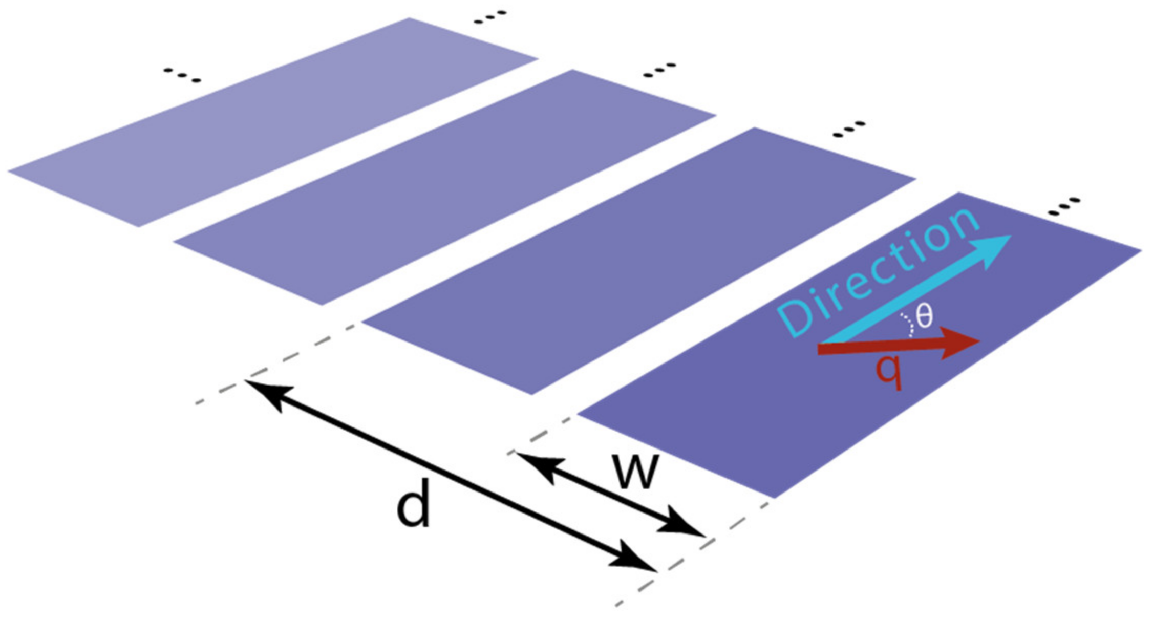
2.2. Semi-Analytical Framework

To begin, Popov et al. [28] show that a series of sub-bands ( E n ) with a bandgap ( Δ ) appear due to the quasi-one-dimensional confinement of the charge carriers in GNRs [33], whose band dispersion can be described by the following equation [34,35]:
E n = ± Δ 2 n 2 + 2 p 2 m Δ
where n is the (sub)band index ( n = 1 ,   2 ,   3 ,   ), m is the effective mass of related charge carriers [28], and p is the parallel momentum. The Δ value can be computed as follows [29]:
Δ = 2   π   v F   w
where is the (reduced) Planck constant and w denotes the ribbon width. Additionally, the m value can be estimated as [29]:
m = Δ 2   v F 2
It is worth noting that Equation (1) offers a quadratic band dispersion and bandgap opening around the Γ point for narrow GNRs and becomes linear, with Δ 0 , as increases the ribbon width, similar to the nature of graphene.
The estimated bandgap ( Δ ) and effective electron masses ( m ) of the systems under study are reported in Table 1.
Let us stress again that GNRs ordered as 2D periodic arrays with a small separation distance between them show similar electronic properties to those of graphene. In fact, SPs are expected to follow the ribbon length instead of the empty space between attached ribbons. In this setting, GNR arrays can be seen as precise 2D planes (see Figure 1) where the group velocity of graphene is the starting parameter that must be correctly assessed before being used in the modeling approach proposed here.
Thus, the v F value ( v F = 0.829 × 10 6 m/s) was previously calculated using DFT computations and applied to determine the plasmon dispersion in GNRs of 2.7 and 100 nm wide [25], demonstrating a significant difference in the plasmon frequency dispersion compared to the conventional value ( v F 10 6 m/s). In Figure S1, this fact is also corroborated for the system under study where the electronic properties can be underestimated/overestimated depending on the value of v F , which in turn affects their plasmonic properties.
Then, the plasmon frequency–momentum dispersion can be estimated by the approach of Ref. [28]:
ω = Re 2   π   e 2   N 2 D ϵ   m q cos   2 θ v 2 4 i v 2
where the electron charge is denoted as e , N 2 D is the 2D electron density, ϵ is the dielectric constant, q is the reciprocal wave vector, θ is the plasmon excitation (Figure 1), and the electron relaxation rate is ascribed as v .
To obtain the plasmon spectrum for selected q values, we apply the conventional approach of the spectral line profile using a Lorentzian function, whose main parameters are described as follows [3]:
L = 1 1 + x 2
where L is the standard Lorentzian function fixed to a maximum value of 1, and x is an auxiliary (dimensionless) variable denoted as:
x = 2 ω ω 0 W
where ω 0 is the transition frequency of the maximum (THz), ω is the frequency/energy regime, and the full width at half maximum (FWHM) is denoted as capital W . W = 0.25 was used for all spectra.
Then, the plasmon spectrum can be plotted by the following expression:
L = 1 1 + 4 ω ω o 2 W 2
We remark on two important facts: (i) Lorentzian line shape functions describe the form of a spectroscopical feature corresponding to a frequency (energy) change in ions, molecules, atoms, or—as in the present case—2D GNR arrays, and (ii) the units of ω , ω 0 , and W are typically wavenumbers (for absorption spectra) or frequency (for lifetime spectrum of collective excitations) [3]. Therefore, we use the last entry, that is, in terms of frequency, what we call the plasmon spectrum, which refers to the plasmon excitation lifetime [3].

3. Results and Discussions

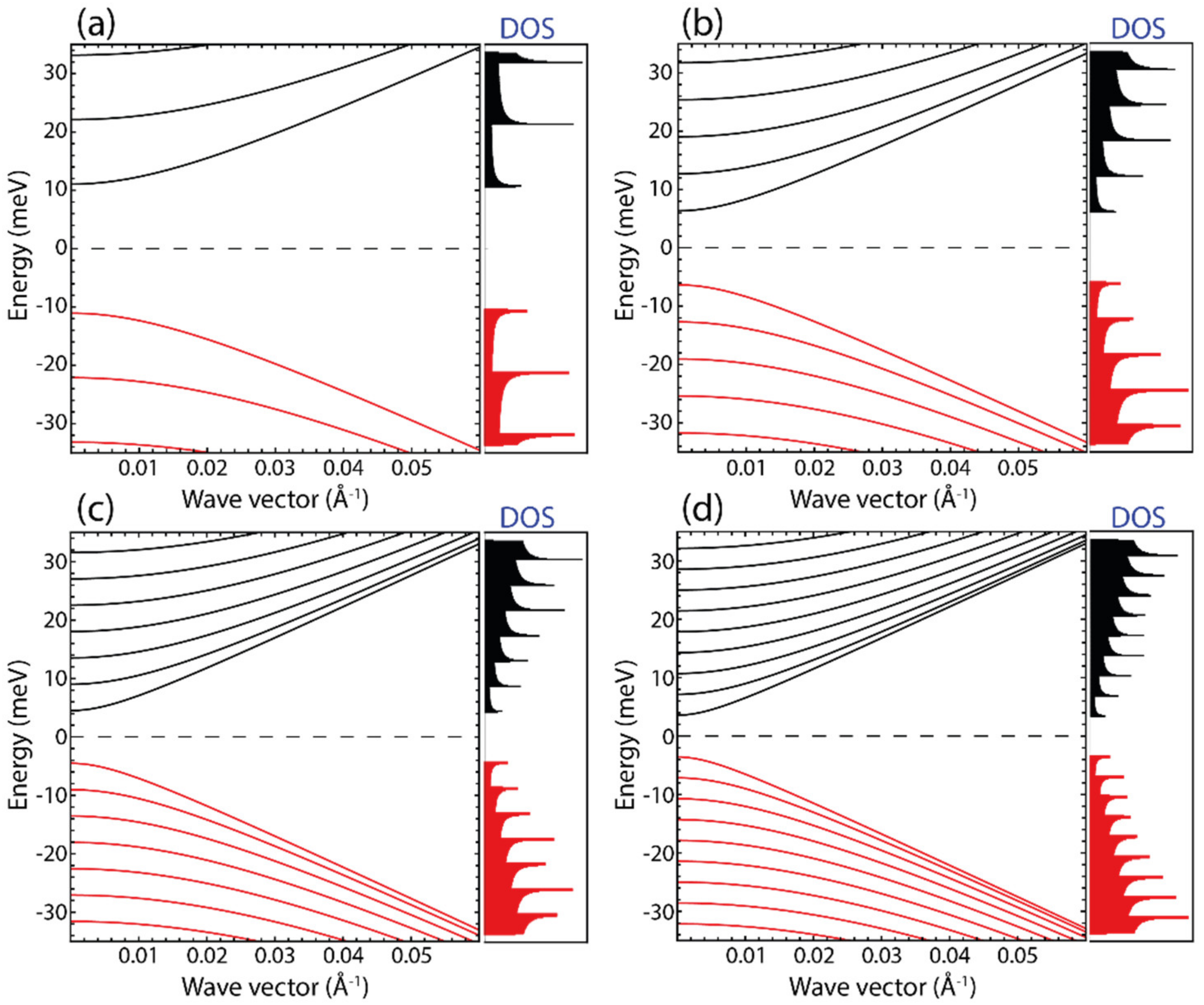
3.1. Bandgap, Band Structure, and Density of States

In Figure 2, we focus on the bandgap ( Δ ) estimated by Equation (2) (with v F = 0.829 × 10 6 m/s [25]) of GNRs under study (155, 270, 380, 480 nm wide [21]) (Figure 2 inset). It is emphasized that we are considering freestanding GNR systems and the effect of the substrate is assumed to be negligible. To clarify this fact, our approach uses the case where the band structure of graphene or GNRs remains unchanged below or above the Fermi level as is well-known when graphene-based materials are grown on insulating substrates (e.g., hexagonal boron nitride).
It is important to mention that the effect of the supporting substrate can be investigated including the corresponding charge carrier velocity and recalculating the effective electron mass.
As expected, in Figure 2, the bandgap decreases as the ribbon width increases. This effect appears independent of the v F (Figure S1). In particular, GNRs under study display very small bandgaps in the order of a few meV: w 155 = 22.12 meV, w 270 = 12.70 meV, w 380 = 9.02 meV, and w 480 = 7.14 meV (see Table 1), suggesting plasmonic responses in the THz scale and related nanophotonic applications such as biosensing. The bandgaps for GNRs from 100 to 500 nm wide are predicted by the orange curve.
To further explore the electronic properties, Figure 3 shows the band structure and density of states (DOS) of GNR systems under study. The corresponding bandgaps and effective electron masses were used in Equation (1) (see Table 1), considering the n index up to 9, i.e., nine valence sub-bands (red curves) and nine conduction sub-bands (black curves).
By this simple model, the estimated effective electron masses (Table 1) are very close to those previously reported [35,36]. More importantly, three interesting facts are evident in Figure 3:
(i)
A direct bandgap at Γ point as observed via DFT computations [20] or GW approximation [36],
(ii)
Several one-dimensional (1D) sub-bands appear in the same energy scale ( ± 30 meV) as the ribbon width increases, giving rise to strong peaks in the DOS,
(iii)
All GNRs seem to be semiconducting materials with the first conduction and last valence bands having a quadratic dispersion around the Γ point.

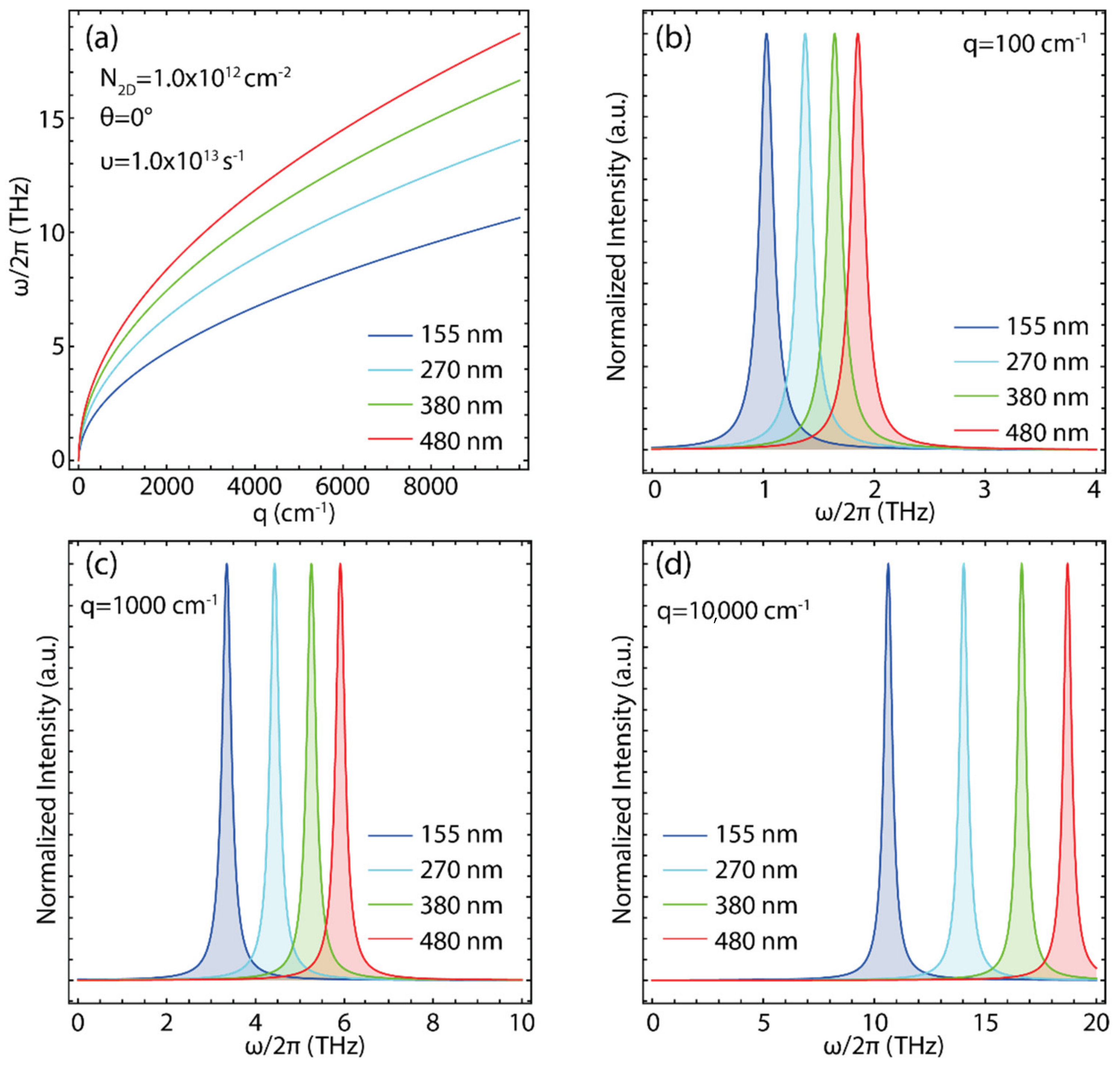
3.2. Plasmonic Properties: Ribbon Width

Previous studies on graphene and related graphene materials [37,38] have demonstrated the existence of two plasmons, an intraband plasmon (so-called SP or 2D plasmon) and an acoustic plasmon at energies below 1 eV. From the technological viewpoint, SP is the most fascinating because its frequency can be manipulated by gating or doping. SP has also been observed in GNR arrays [21] and confirmed via TDDFT computations [20], in both cases working on the eV scale.
In a comparative effort between the numerical computations using DFT/TDDFT+RPA [20] and the semi-analytical model used here, Figure S5 elucidates the electronic properties of wide and ultra-narrow GNRs at the experimental and theoretical levels. In particular, Figure S5b shows interesting results of the semi-analytical model when predicting the bandgap for different families of GNRs of up to 3 nm wide in comparison with the DFT/GW approximation [36]. With this in mind, the five-armchair graphene nanoribbon (5AGNR) ( w 1 nm and family 3p + 2) was selected as the testing system. Interestingly enough, a perfect agreement for N 2 D 3.67 × 10 12 cm−2 is observed for the plasmon frequency dispersion (Figure S6), demonstrating the adaptability of the proposed semi-analytical model to scrutinize ultra-narrow ribbons. To estimate the corresponding charge carrier density in 5AGNR, we return to the concept of the Fermi level discussed later (Section 3.5)
We now focus on the tunability of the SP in the THz scale (Figure 4, Figure 5, Figure 6, Figure 7, Figure 8, Figure 9 and Figure 10), where most of the graphene plasmonics is projected [39]. Beyond the doping effect that is associated with the charge carrier concentration ( N 2 D ), we evidence an extra controllability of the SP by changing the ribbon width ( w ), plasmon excitation angle ( θ ), and electron relaxation rate ( ν ).
Keeping this in mind, Figure 4 shows the plasmon frequency dispersion of the experimentally realized 2D GNR arrays under study (Figure 1 inset). Based on Ref. [40], we fix the values of N 2 D = 1.0 × 10 12 cm−2, ν = 1.0 × 10 13 s−1, and θ = 0 .
Interestingly, the trend of the curves is unaffected by the ribbon width, exposing a q -like plasmon dispersion as is typical of 2D systems. Another important result is the fact that increasing the ribbon width increases the plasmon frequency with values of up to 20 THz. To highlight this fact, the plasmon frequency spectra for selected q values are reported in Figure 4b–d and Table 2. The plasmon spectra were obtained by the approach of the Lorentzian line shape function (i.e., spectral line profile) to a maximum value of 1 with the corresponding transition energy (THz) extracted from the plasmon frequency–momentum data.
On the other hand, for q = 100 cm−1, the maximum of the plasmon peak moves from 1.03 to 1.85 THz (Figure 4b), and for q = 1000 cm−1, from 3.35 to 5.91 THz (Figure 4c). At the first approximation, the greatest increase in frequency is observed at q = 10,000 cm−1, giving a plasmon response from 10.63 to 18.71 THz (Figure 4d).
A close look at the increase in plasmon frequency shows that regardless of the value of q (Table 3), the frequency increases by ~ 25% for systems from 155 nm to 270 nm, ~ 16% from 270 nm to 380 nm, and by ~ 11% from 380 nm to 480 nm. These results allow us to conclude that there is a relative inverse relationship between the ribbon width and the plasmon frequency, that is, as the ribbon width increases, the effect on the plasmon frequency dispersion becomes gradually minor.
From a strict statistical aspect, in Table 3, one can see that the average change in the plasmon frequency rate as a function of the width variation, from the narrowest ( w = 155 nm) to the widest ( w = 480 nm) GNR, is 17.5% for q = 100 cm−1, 17.1% for q = 1000 cm−1, and 17.6% for q = 10,000 cm−1. These results suggest a constant trend of the plasmon frequency regardless of the value of q , suggesting a slight effect on the ribbon width.

3.3. Plasmonic Properties: Excitation Angle

We now proceed to analyze the consequence of the plasmon excitation angle. Specifically, Figure 5 displays the plasmon frequency–momentum dispersion for 2D GNR arrays by taking different directions for the excitation wave vector: θ = 0 ° (black line), θ = 60 ° (blue line), and θ = 80 ° (red line). Different ribbon widths are considered: w = 155 nm (Figure 5a), w = 270 nm (Figure 5b), w = 380 nm (Figure 5c), and w = 480 nm (Figure 5d). N 2 D = 1.0 × 10 12 cm−2 and ν = 1.0 × 10 13 s−1 are fixed.
As observed, a q -like dispersion is preserved in all 2D GNR arrays regardless of excitation angle. Interestingly enough, plasmons are not detected in some cases since the radicand in Equation (4) becomes negative. To clarify this fact, collective oscillations, i.e., plasmons, are dictated by the zeros in the real part of the macroscopic dielectric function [37]:
ϵ M q , ω = 1 ϵ 1 q , ω
in a frequency range where the imaginary part is small or zero. Then, if this plasmon condition is not met, only single-particle excitations can be found instead of collective excitations. Taking this into account, we discuss all cases where the plasmon may or may not exist.
In particular, at θ = 80 , no plasmon is found at q < 1200 cm−1 for w = 155 nm, at q < 700 cm−1 for w = 270 nm, at q < 500 cm−1 for w = 380 nm, and at q < 400 cm−1 for w = 480 nm. As the ribbon width increases, the momentum region for which the plasmon does not exist shrinks, suggesting that for w , the frequency dispersion recuperates the result of ideal 2D materials, i.e., frequency–momentum dispersion starting at THz = 0 and q = 0 . Additionally, for w = 155 nm (Figure 5a), the entire frequency–momentum dispersion is below 25 THz, whereas for w = 480 nm (Figure 5d), the entire plasmon dispersion is below 40 THz.
To extra-analyze the crucial fact of the excitation angle at θ = 80 , the maximum of the plasmon peak for selected q values and different ribbon widths are reported in Table 4 and Figure S2a–d.
As mentioned above, for the sampled momentum range, no plasmon is observed for q = 1000 cm−1 in 2D GNR arrays of 155 nm wide (Figure 5a, Table 4). Explicitly, the maximum of the plasmon peak is found for w = 155 nm from 1.05 to 3.43 THz (Figure S2a), for w = 270 nm from 0.87 to 4.65 THz (Figure S2b), for w = 380 nm from 1.31 to 5.58 THz (Figure S2c), and for w = 480 nm from 1.60 to 6.30 THz (Figure S2d). To highlight the results of the excitation angle at θ = 80 , Figure 6 and Table 5 show that the highest result of the combination of excitation angle and ribbon width occurs at small q values, say, q = 2000 cm−1. Actually, the frequency increases by ~40% for systems from 155 nm to 270 nm, ~22% from 270 nm to 380 nm, and by ~14% from 380 nm to 480 nm (Table 5).
Table 5 shows that the average change in the plasmon frequency rate vs. the width variation, from the narrowest ( w = 155 nm) to the widest ( w = 480 nm) GNR, is 25.1% for q = 2000 cm−1, 19.4% for q = 5000 cm−1, and 18.1% for q = 10,000 cm−1. These results evidence a decreasing trend of the plasmon frequency as a function of the value of q , suggesting an appreciable effect of the combination of ribbon width and excitation angle at θ = 80 .

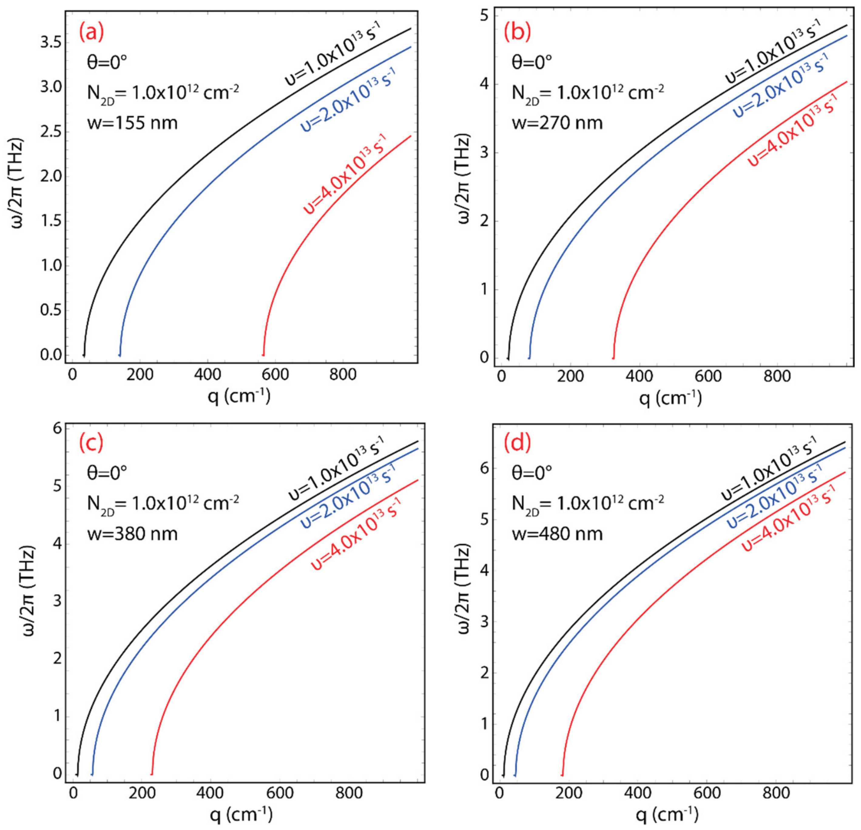
3.4. Plasmonic Properties: Electron Relaxation Rate

Depending on the synthesis process, the preparation of graphene (or related honeycomb-like materials) gives samples with different types of defects, e.g., sp3, vacancy-like, and edge defects [41]. Noticeably, these types of defects are expected in wide GNRs and greatly influence their physical and chemical properties [42]. As a crucial case for the present work, high carrier mobility is commonly measured in defect-free samples; however, as the density of defects increases, the charge carrier mobility becomes poor. In Figure 7, this is precisely what we inspect by changing the value of ν , keeping in mind the following idea: a high value of ν is due to the fact that a higher concentration of defects gives a low charge carrier mobility.
The sensitivity of the frequency–momentum dispersion is examined using three typical values of ν ( ν = 1.0 × 10 13 s−1 (black curve), ν = 2.0 × 10 13 s−1 (blue curve), and ν = 4.0 × 10 13 s−1 (red curve)) and fixing N 2 D = 1.0 × 10 12 cm−2 and θ = 0 . Note that the horizontal scale of Figure 7a–d is 10 times smaller compared to previous Figures.
In all cases, by increasing the value of ν , the frequency–momentum dispersion shift toward larger values of q as well as the plasmon frequency is reduced. Once more, an important result is a fact that there is a momentum range for which plasmons are not detected at ν = 2.0 × 10 13 s−1 and ν = 4.0 × 10 13 s−1. Particularly, the greatest effect of the relaxation rate is notable at ν = 4.0 × 10 13 s−1 where no plasmon is found at q < 550 cm−1 for w = 155 nm, at q < 350 cm−1 for w = 270 nm, at q < 250 cm−1 for w = 380 nm, and at q < 200 cm−1 for w = 480 nm. An extra result is a fact that increasing the ribbon width slightly increases the plasmon frequency from about 3.5 to 6.5 THz.
To further emphasize the result of the relaxation rate at ν = 4.0 × 10 13 s−1, the maxima of the plasmon peak for selected q values and considering different ribbon widths are reported in Figure S3a–d and Table 6. We evidence that for the sampled momentum range, no plasmon is observed for q = 100 cm−1 in all 2D GNR arrays. More importantly, the maximum of the plasmon peak is detected for w = 155 nm from 0.69 to 2.45 THz (Figure S3a), for w = 270 nm from 1.35 to 4.04 THz (Figure S3b), for w = 380 nm from 1.53 to 5.11 THz (Figure S3c), and for w = 480 nm from 0.86 to 5.92 THz (Figure S3d).
These results confirm that the highest effect of the relaxation rate is on the starting momentum region of the plasmon response and not on the plasmon frequency since this is reduced by approximately 1 THz at ν = 4.0 × 10 13 s−1 (red curves, see Figure 7) compared to ν = 1.0 × 10 13 s−1 (black curves, see Figure 7). Hence, a low density of defects (i.e., low ν values) results in a smaller forbidden momentum region.
On the other hand, Figure 8 and Table 7 confirm that the highest effect of the combination of relaxation rate ( ν = 4.0 × 10 13 s−1) and ribbon width, particularly, occurs at q = 600 cm−1. The frequency increases by ~73% for GNR arrays from 155 nm to 270 nm, ~27% from 270 nm to 380 nm, and by ~16% from 380 nm to 480 nm.
Table 7 displays that the average change in the plasmon frequency rate vs. the width variation, from the narrowest GNR ( w = 155 nm) to the widest GNR ( w = 480 nm), is 38.9% for q = 600 cm−1, 28.1% for q = 800 cm−1, and 24.7% for q = 1000 cm−1. These results indicate a decreasing trend of the plasmon frequency as a function of the value of q , suggesting a significant effect of the combination of ribbon width and electron relaxation rate at ν = 4.0 × 10 13 s−1. This effect is even superior to the two previously discussed cases.

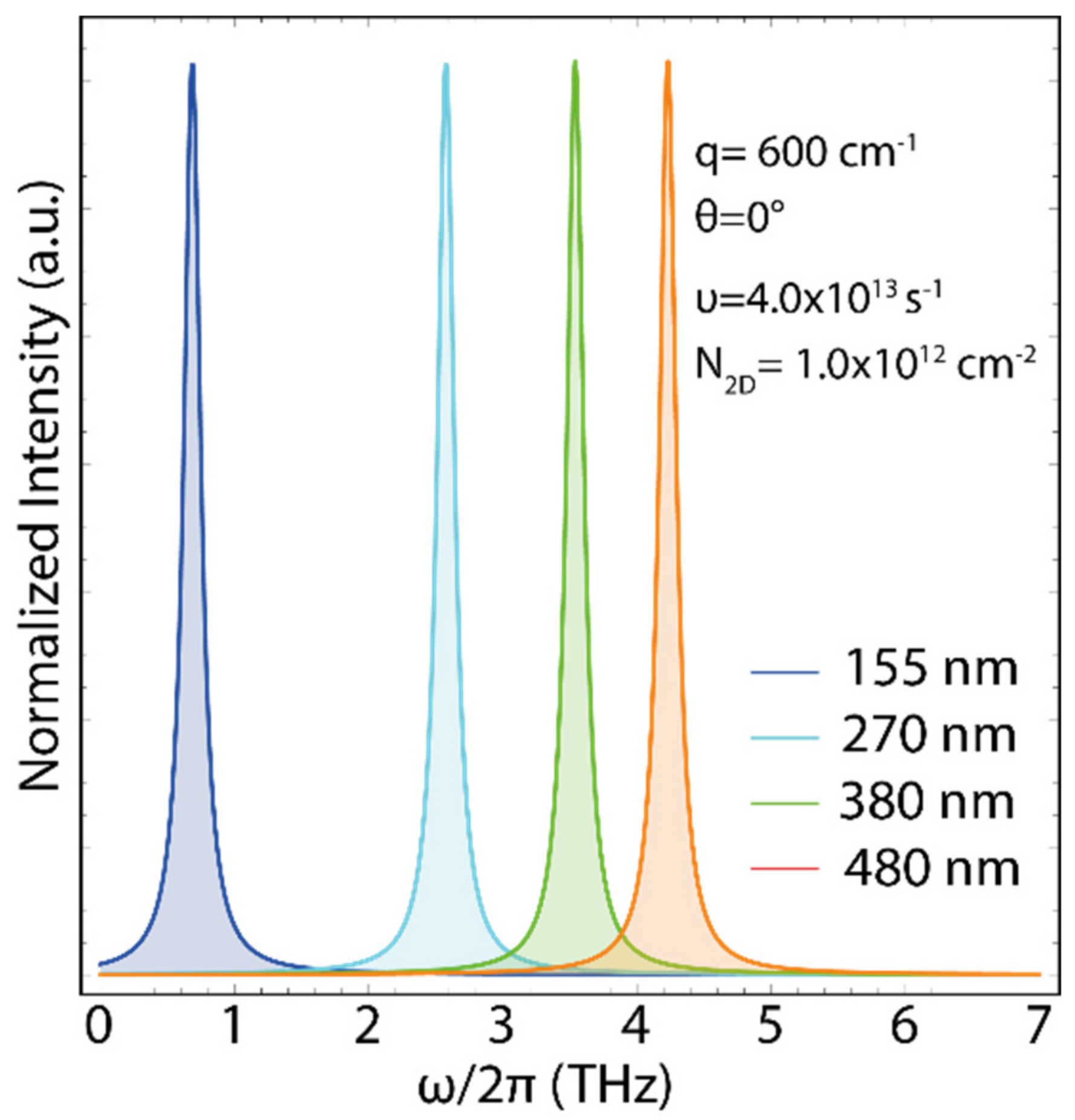
3.5. Plasmonic Properties: Charge Carrier Density

Another important parameter to be measured is the charge carrier concentration, which in the present modeling approach is described by the 2D charge carrier density ( N 2 D ). This parameter can be adapted by doping the GNRs or by a gating voltage, i.e., by injecting or ejecting electrons.
While the charge carrier density ( N 2 D ) can be extracted from the expression of the Fermi level ( E F ) [32,40]:
E F =   v F 2   π   N 2 D
here it is decided to use the quantities of previous measures. In particular, this quantity can vary easily up to N 2 D ~ 5.0 × 10 12 cm−2 [35]. In Figure 9, we focus precisely on the effect of charge carrier density on the plasmon frequency–momentum dispersion for each of the systems ( w = 155 nm (Figure 9a), w = 270 nm (Figure 9b), w = 380 nm (Figure 9c), and w = 480 nm (Figure 9d)) by using three reference N 2 D values ( N 2 D = 1.0 × 10 12 cm−2 (black curve), N 2 D = 1.0 × 10 12 cm−2 (blue curve), and N 2 D = 1.0 × 10 12 cm−2 (red curve)), and fixing ν = 1.0 × 10 13 s−1 and θ = 0 .
As stated, Figure 9 shows the plasmon frequency dispersion of the systems under study as a function of different charge carrier densities. This effect is very dramatic for the frequency dispersion in all analyzed cases because increasing the charge carrier density leads to an increase in the plasmon frequency. Specifically, a noteworthy increase in frequency is observed, from ν = 1.0 × 10 13 s−1 (black curves) to ν = 4.0 × 10 13 s−1 (red curves), of about 10 THz for 2D GNR arrays of 155 nm wide, ~ 15 THz for 270 nm wide, ~ 20 THz for 380 nm wide, and ~ 25 THz for 480 nm wide. This effect has also been corroborated by TFDFT calculations on the eV scale [20,22], considering very narrow 2D GNR arrays ( w < 2 nm). As in the previously analyzed parameters, all the curves show a q -like plasmon dispersion independent of the charge carrier density or the ribbon width.
To inspect the central fact of the charge carrier density at N 2 D = 4.0 × 10 12 cm−2 on all systems under study, the maximum of the plasmon peak for selected q values are reported in Figure S4a–d and Table 8.
As observed, the maximum of the plasmon peak is found below 40 THz with a plasmon response from 6.72 to 21.26 THz for w = 155 nm (Figure S4a), from 8.87 to 28.06 THz for w = 270 nm (Figure S4b), from 10.53 to 33.29 THz for w = 380 nm (Figure S4c), and from 11.83 to 37.42 THz for w = 480 nm (Figure S4d). These numerical results demonstrate the important result of the 2D charge carrier density on the plasmon frequency, particularly compared to N 2 D = 1.0 × 10 12 cm−2, where the plasmon frequency dispersion is found below 15 THz (Figure 9, black curves).
Regardless of the value of q , Table 9 shows that the combined effect of charge carrier density and ribbon width increased the frequency by ~ 24% for systems from 155 nm to 270 nm, ~ 16% from 270 nm to 380 nm, and ~ 11% from 380 nm to 480 nm. The latter also confirms that as the ribbon width increases, the effect on the frequency dispersion gradually becomes smaller (see e.g., Figure 10), suggesting that in graphene (or related 2D nanomaterials) the plasmon frequency should be even lower for w .
Table 9 exhibits that the average change in the plasmon frequency rate vs. the width variation, from the narrowest GNR ( w = 155 nm) to the widest GNR ( w = 480 nm), is 17.0% for q = 1000 cm−1, 17.0% for q = 5000 cm−1, and 17.0% for q = 10,000 cm−1. These results indicate a constant trend of the plasmon frequency as a function of the value of q , suggesting a negligible effect of the combination of ribbon width and charge density concentration at N 2 D = 4.0 × 10 12 cm−2.

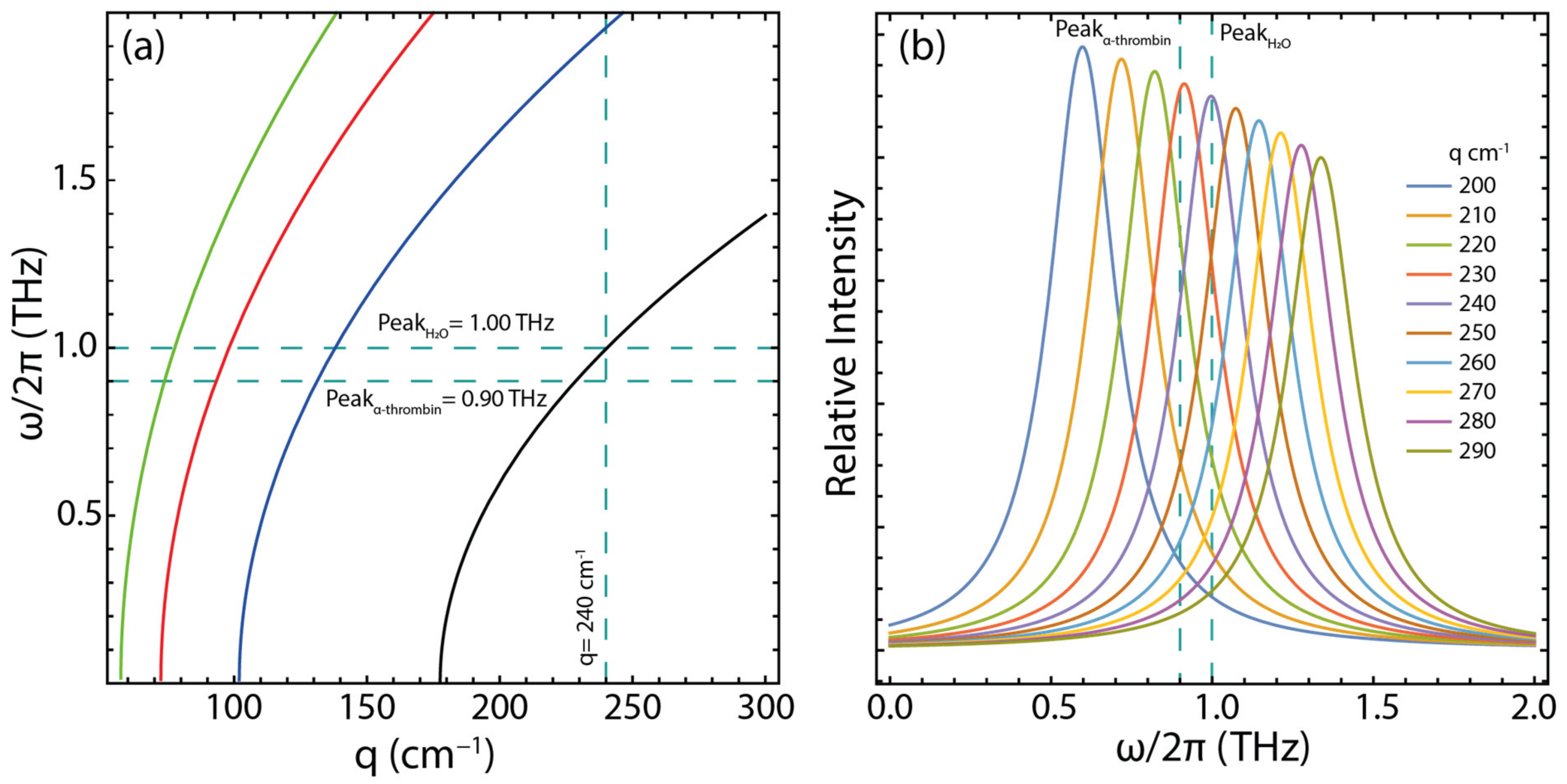
4. Applications in Molecular Sensing of Aqueous Molecules

An important application, in terms of quantifiable examination, is the identification of molecules in water because this medium produces high THz absorption (at 1 THz and q 240 cm−1 [43]). Water obscures the response of molecules, leading to similar absorption features for different pure molecules. To disappear this interference, samples have to be dried or the water medium must be replaced. Nevertheless, these strategies are not possible to perform in all cases. Hence, novel materials with resonances in the water frequency absorption regime could importantly improve the interactions between adherent target molecules and incident THz waves, demonstrating practical applications in (bio)sensing.
Figure 11 demonstrates the possibility of using 2D GNR arrays to address these issues, by using N 2 D = 1.0 × 10 12 cm−2, θ = 0 , and ν = 2.24 s−1. Note that a high value of the relaxation rate ( ν ) is used to be able to achieve the desired frequency (1 THz) and momentum ( q 240 cm−1), demonstrating that GNRs with a high defect concentration could be the best platforms for detecting pure molecules in water.
Specifically, Figure 11a demonstrates that molecules in water can be detected by using 2D GNR arrays of 155 nm wide (black curve), setting the possibility of assembling enhanced THz biosensors to sense, for instance, human α thrombin, whose resonance peak is detected at about 0.9 THz [43]. To further emphasize this finding, Figure 11b confirms the existence of resonance modes in the same THz frequency of water at q = 240 cm−1 (purple curve) and α thrombin at q = 229 cm−1 (red curve).
More importantly, this exploratory application shows that 2D GNR arrays are excellent platforms to support SP propagation at the THz scale (below 1 THz) and can be assembled into more complex and compact devices, such as biosensors, for example, prism-coupled biosensors [44], fiber-coupled biosensors [45], grating-coupled biosensors [46], nanoparticle-coupled biosensors [47], plasmon-coupled emission biosensors [48], and surface-enhanced Raman-scattering biosensors [49], as well as for THz band communications ( 1 THz) such as graphene-based plasmonic nano-transceivers [50] and graphene-based plasmonic nano-antennas [51].

5. Conclusions

Using a semi-analytical modeling approach and the group velocity of graphene, in the present study, we explored the electronic and plasmonic properties of experimentally realized GNRs organized in a periodic array within the terahertz scale ( 40 THz) by considering free-standing models.
Although this approach shows obvious limitations such as the frequency (energy) range of application and non-atomistic effects considered (nanoribbon edges), it allows the analysis of trends of plasmon frequency dispersion in wide GNRs, for which an ab initio approach is infeasible because of a large number of carbons. However, this approach can be adapted for different studies or systems by simply estimating the charge carrier velocity and recalculating the effective electron mass. Our results provide a complete picture of controlling the plasmon frequency and the frequency–momentum dispersion.
In particular, these plasmonic properties are strongly dependent on ribbon width (155, 270, 380, 480 nm), charge carrier density ( 1.0 × 10 12 cm−2, 2.0 × 10 12 cm−2, and 4.0 × 10 12 cm−2), and electron relaxation rate ( 1.0 × 10 13 s−1, 2.0 × 10 13 s−1, and 4.0 × 10 13 s−1). Other factors such as Fermi level shift or temperature can be manipulated from Equation (9) and used in Equation (4).
The main findings:
  • The GNR systems considered show bandgap values of a few meV ( ~ 22 meV for w = 155 nm, ~ 13 meV for w = 270 nm, ~ 9 meV for w = 380 nm, and ~ 7 meV for w = 480 nm).
  • The bandgap values decrease as the ribbon widths increase, with a trend that follows an exponentially decreasing behavior.
  • The increase in the ribbon width raises the plasmon frequency up to about 20 THz for w = 155 nm and up to about 40 THz for w = 480 nm.
  • The combination of the ribbon width plus the electro-relaxation rate seems to be the most critical aspect affecting the plasmonic properties because the plasmon frequency is noticeably reduced and shifted to higher values of q .
  • Forbidden plasmon regions can be observed by changing the electron relaxation rate and plasmon excitation angle.
Additionally, we discuss the potential application in the molecular sensing of pure aqueous molecules such as human α thrombin at very low frequencies (<2 THz).
  • The study is restricted to this frequency regime because the water generates strong THz absorption at 1 THz, which severely obscures the response of molecules.
  • Two-dimensional GNR arrays of 155 nm wide seem to be interesting platforms to solve this issue because these systems show resonance peaks in the same water frequency absorption region.
  • Then, any biological molecule could be directly detected in water without altering the sample via drying processes.
We emphasize again that the semi-analytical model is used to solve the obvious technical limitations of atomistic approaches when treating wide GNRs, which cannot be addressed with current calculators around the world. We further remark that these novel features require experiments, in line with what has been reported here, for a correct tuning of the input parameters of possible GNR arrays-based devices or other materials beyond graphene [52].

Supplementary Materials

The following supporting information can be downloaded at: https://www.mdpi.com/article/10.3390/coatings13010028/s1, Figure S1: Bandgap ( Δ ) as a function of the ribbon width ( w ), considering the charge carrier velocity computed by DFT-LDA ( v F = 0.829 × 10 6 m/s) (Ref. [25] in the main text) and the conventional value widely used ( v F 10 6 m/s) (Ref. [28] in the main text). Markers represent the GNR systems under study and continue lines are the fitting curve using Equation 2 (in the main text).; Figure S2. Plasmon frequency ( ω / 2 π 7 THz) (using θ = 80 , N 2 D = 1.0 × 10 12 cm−2, ν = 1.0 × 10 13 s−1, and v F = 0.829 × 10 6 m/s) for selected q values from 1000 to 10,000 cm−1, with different ribbon widths: (a) w = 155 nm, (b) w = 270 nm, (c) w = 380 nm, and (d) w = 480 nm. Plasmon spectra were constructed using the Lorentz line shape function to a maximum value of 1, setting the full width at half maximum to 0.2, and the corresponding transition frequency was taken from Table 4 (in the main text) for the selected q values. A conventional exponential decay function is adopted for the dispersion of the plasmon spectra.; Figure S3. Plasmon frequency ( ω / 2 π 7 THz) (using θ = 0 , N 2 D = 1.0 × 10 12 cm−2, ν = 4.0 × 10 13 s−1, and v F = 0.829 × 10 6 m/s) for selected q values from 100 to 1000 cm−1, with different ribbon widths: (a) w = 155 nm, (b) w = 270 nm, (c) w = 380 nm, and (c) w = 480 nm. Plasmon spectra were constructed using the Lorentz line shape function to a maximum value of 1, setting the full width at half maximum to 0.2, and the corresponding transition frequency was taken from Table 6 (in the main text) for the selected q values. A conventional exponential decay function is adopted for the dispersion of the plasmon spectra.; Figure S4. Plasmon frequency ( ω / 2 π 40 THz) (using θ = 0 , N 2 D = 4.0 × 10 12 cm−2, ν = 1.0 × 10 13 s−1, and v F = 0.829 × 10 6 m/s) for selected q values from 1000 to 10,000 cm−1, with different ribbon widths: (a) w = 155 nm, (b) w = 270 nm, (c) w = 380 nm, and (c) w = 480 nm. Plasmon spectra were constructed using the Lorentz line shape function to a maximum value of 1, setting the full width at half maximum to 0.2, and the corresponding transition frequency was taken from Table 8 (in the main text) for the selected q values. A conventional exponential decay function is adopted for the dispersion of the plasmon spectra; Figure S5. Bandgap as a function of ribbon width. (a) Experimental results for different datasets (P1-P4) and (b) GW approximation for different families of GNRs (Ref. [29] in the main text). The red line is the predicted curve using Equation (2) (in the main text).; Figure S6. Plasmon frequency dispersion ( ω / 2 π ) vs. wave vector ( q ) for five armchair graphene nanoribbon (5AGNR), considering the numerical TDDFT+RPA approach (Ref. [20] in the main text) and the predictions of the semi-analytical model through Equation (4). The input parameters of Equation (4) are given in the figure.

Author Contributions

Conceptualization, supervision, C.V.G.; methodology, Y.C. and C.V.G.; validation, T.T., S.B. and M.G.; investigation, M.Á.S.P. and C.V.G.; resources, T.T.; data curation, T.T. and M.G.; writing—original draft preparation, C.V.G.; writing—review and editing, S.B. and C.V.G.; visualization, M.G. All authors have read and agreed to the published version of the manuscript.

Funding

This work was supported by Universidad Técnica Particular de Loja (UTPL-Ecuador) (RUC 1190068729001).

Institutional Review Board Statement

Not Applicable.

Informed Consent Statement

Not applicable.

Data Availability Statement

The authors declare that the data supporting the fundings of this study are available within the paper (and its Supplementary Materials files). Further data are also available from the corresponding author upon reasonable request.

Acknowledgments

T.T., M.G. and C.V.G. wish to thank the Ecuadorian National Department of Sciences and Technology (SENESCYT).

Conflicts of Interest

The authors declare no conflict of interest.

References

  1. Economou, E.N. Surface Plasmons in Thin Films. Phys. Rev. 1969, 182, 539. [Google Scholar] [CrossRef]
  2. Altug, H.; Oh, S.-H.; Maier, S.A.; Homola, J. Advances and Applications of Nanophotonic Biosensors. Nat. Nanotechnol. 2022, 17, 5–16. [Google Scholar] [CrossRef]
  3. Tene, T.; Guevara, M.; Svozilík, J.; Coello-Fiallos, D.; Briceño, J.; Vacacela Gomez, C. Proving Surface Plasmons in Graphene Nanoribbons Organized as 2D Periodic Arrays and Potential Applications in Biosensors. Chemosensors 2022, 10, 514. [Google Scholar] [CrossRef]
  4. Abir, T.; Tal, M.; Ellenbogen, T. Second-Harmonic Enhancement from a Nonlinear Plasmonic Metasurface Coupled to an Optical Waveguide. Nano Lett. 2022, 22, 2712–2717. [Google Scholar] [CrossRef] [PubMed]
  5. Ali, A.; El-Mellouhi, F.; Mitra, A.; Aissa, B. Research Progress of Plasmonic Nanostructure-Enhanced Photovoltaic Solar Cells. Nanomaterials 2022, 12, 788. [Google Scholar] [CrossRef] [PubMed]
  6. Wang, Y.; Chen, K.; Lin, Y.-S.; Yang, B.-R. Plasmonic Metasurface with Quadrilateral Truncated Cones for Visible Perfect Absorber. Phys. E Low-Dimens. Syst. Nanostruct. 2022, 139, 115140. [Google Scholar] [CrossRef]
  7. Sayed, M.; Yu, J.; Liu, G.; Jaroniec, M. Non-Noble Plasmonic Metal-Based Photocatalysts. Chem. Rev. 2022, 122, 10484–10537. [Google Scholar] [CrossRef]
  8. Low, T.; Avouris, P. Graphene Plasmonics for Terahertz to Mid-Infrared Applications. ACS Nano 2014, 8, 1086–1101. [Google Scholar] [CrossRef] [Green Version]
  9. Chen, J.; Badioli, M.; Alonso-González, P.; Thongrattanasiri, S.; Huth, F.; Osmond, J.; Spasenović, M.; Centeno, A.; Pesquera, A.; Godignon, P.; et al. Optical Nano-Imaging of Gate-Tunable Graphene Plasmons. Nature 2012, 487, 77–81. [Google Scholar] [CrossRef] [Green Version]
  10. Gomez, C.V.; Pisarra, M.; Gravina, M.; Sindona, A. Tunable Plasmons in Regular Planar Arrays of Graphene Nanoribbons with Armchair and Zigzag-Shaped Edges. Beilstein J. Nanotechnol. 2017, 8, 172–182. [Google Scholar] [CrossRef]
  11. Coello-Fiallos, D.; Tene, T.; Guayllas, J.L.; Haro, D.; Haro, A.; Gomez, C.V. DFT Comparison of Structural and Electronic Properties of Graphene and Germanene: Monolayer and Bilayer Systems. Mater. Today Proc. 2017, 4, 6835–6841. [Google Scholar] [CrossRef]
  12. Avouris, P.; Dimitrakopoulos, C. Graphene: Synthesis and Applications. Mater. Today 2012, 15, 86–97. [Google Scholar] [CrossRef]
  13. Villamagua, L.; Carini, M.; Stashans, A.; Gomez, C.V. Band Gap Engineering of Graphene through Quantum Confinement and Edge Distortions. Ric. Mat. 2016, 65, 579–584. [Google Scholar] [CrossRef]
  14. Dutta, S.; Pati, S.K. Novel Properties of Graphene Nanoribbons: A Review. J. Mater. Chem. 2010, 20, 8207–8223. [Google Scholar] [CrossRef]
  15. Wang, J.; Zhao, R.; Yang, M.; Liu, Z.; Liu, Z. Inverse Relationship between Carrier Mobility and Bandgap in Graphene. J. Chem. Phys. 2013, 138, 84701. [Google Scholar] [CrossRef] [PubMed] [Green Version]
  16. Kang, J.W.; Lee, J.H.; Hwang, H.J.; Kim, K.-S. Developing Accelerometer Based on Graphene Nanoribbon Resonators. Phys. Lett. A 2012, 376, 3248–3255. [Google Scholar] [CrossRef]
  17. Wang, X.; Ouyang, Y.; Li, X.; Wang, H.; Guo, J.; Dai, H. Room-Temperature All-Semiconducting Sub-10-Nm Graphene Nanoribbon Field-Effect Transistors. Phys. Rev. Lett. 2008, 100, 206803. [Google Scholar] [CrossRef] [PubMed] [Green Version]
  18. Karimi, F.; Knezevic, I. Plasmons in Graphene Nanoribbons. Phys. Rev. B 2017, 96, 125417. [Google Scholar] [CrossRef] [Green Version]
  19. Aguillon, F.; Marinica, D.C.; Borisov, A.G. Atomic-Scale Control of Plasmon Modes in Graphene Nanoribbons. Phys. Rev. B 2022, 105, L081401. [Google Scholar] [CrossRef]
  20. Gomez, C.V.; Pisarra, M.; Gravina, M.; Pitarke, J.M.; Sindona, A. Plasmon Modes of Graphene Nanoribbons with Periodic Planar Arrangements. Phys. Rev. Lett. 2016, 117, 116801. [Google Scholar]
  21. Fei, Z.; Goldflam, M.D.; Wu, J.-S.; Dai, S.; Wagner, M.; McLeod, A.S.; Liu, M.K.; Post, K.W.; Zhu, S.; Janssen, G.; et al. Edge and Surface Plasmons in Graphene Nanoribbons. Nano Lett. 2015, 15, 8271–8276. [Google Scholar] [CrossRef] [PubMed]
  22. Sindona, A.; Pisarra, M.; Bellucci, S.; Tene, T.; Guevara, M.; Gomez, C.V. Plasmon Oscillations in Two-Dimensional Arrays of Ultranarrow Graphene Nanoribbons. Phys. Rev. B 2019, 100, 235422. [Google Scholar] [CrossRef]
  23. Sindona, A.; Vacacela Gomez, C.; Pisarra, M. Dielectric Screening versus Geometry Deformation in Two-Dimensional Allotropes of Silicon and Germanium. Sci. Rep. 2022, 12, 1–12. [Google Scholar] [CrossRef] [PubMed]
  24. Gomez, C.V.; Pisarra, M.; Gravina, M.; Riccardi, P.; Sindona, A. Plasmon Properties and Hybridization Effects in Silicene. Phys. Rev. B 2017, 95, 85419. [Google Scholar]
  25. Tene, T.; Guevara, M.; Viteri, E.; Maldonado, A.; Pisarra, M.; Sindona, A.; Vacacela Gomez, C.; Bellucci, S. Calibration of Fermi Velocity to Explore the Plasmonic Character of Graphene Nanoribbon Arrays by a Semi-Analytical Model. Nanomaterials 2022, 12, 2028. [Google Scholar] [CrossRef] [PubMed]
  26. Lin, M.-W.; Ling, C.; Zhang, Y.; Yoon, H.J.; Cheng, M.M.-C.; Agapito, L.A.; Kioussis, N.; Widjaja, N.; Zhou, Z. Room-Temperature High on/off Ratio in Suspended Graphene Nanoribbon Field-Effect Transistors. Nanotechnology 2011, 22, 265201. [Google Scholar] [CrossRef] [Green Version]
  27. Hu, H.; Yu, R.; Teng, H.; Hu, D.; Chen, N.; Qu, Y.; Yang, X.; Chen, X.; McLeod, A.S.; Alonso-González, P.; et al. Active Control of Micrometer Plasmon Propagation in Suspended Graphene. Nat. Commun. 2022, 13, 1–9. [Google Scholar] [CrossRef]
  28. Popov, V.V.; Bagaeva, T.Y.; Otsuji, T.; Ryzhii, V. Oblique Terahertz Plasmons in Graphene Nanoribbon Arrays. Phys. Rev. B 2010, 81, 73404. [Google Scholar] [CrossRef]
  29. Gomez, C.V.; Guevara, M.; Tene, T.; Lechon, L.S.; Merino, B.; Brito, H.; Bellucci, S. Energy Gap in Graphene and Silicene Nanoribbons: A Semiclassical Approach. In Proceedings of the 2nd International Congress on Physics ESPOCH (ICPE-2017), Riobamba, Ecuador, 6–8 December 2017; Volume 2003, p. 20015. [Google Scholar]
  30. Gonze, X.; Amadon, B.; Anglade, P.-M.; Beuken, J.-M.; Bottin, F.; Boulanger, P.; Bruneval, F.; Caliste, D.; Caracas, R.; Côté, M.; et al. ABINIT: First-Principles Approach to Material and Nanosystem Properties. Comput. Phys. Commun. 2009, 180, 2582–2615. [Google Scholar] [CrossRef]
  31. Kohn, W. Density-Functional Theory for Excited States in a Quasi-Local-Density Approximation. Phys. Rev. A 1986, 34, 737. [Google Scholar] [CrossRef]
  32. Hwang, C.; Siegel, D.A.; Mo, S.-K.; Regan, W.; Ismach, A.; Zhang, Y.; Zettl, A.; Lanzara, A. Fermi Velocity Engineering in Graphene by Substrate Modification. Sci. Rep. 2012, 2, 590. [Google Scholar] [CrossRef] [Green Version]
  33. Sindona, A.; Pisarra, M.; Gomez, C.V.; Riccardi, P.; Falcone, G.; Bellucci, S. Calibration of the Fine-Structure Constant of Graphene by Time-Dependent Density-Functional Theory. Phys. Rev. B 2017, 96, 201408. [Google Scholar] [CrossRef]
  34. Barone, V.; Hod, O.; Scuseria, G.E. Electronic Structure and Stability of Semiconducting Graphene Nanoribbons. Nano Lett. 2006, 6, 2748–2754. [Google Scholar] [CrossRef] [PubMed]
  35. Han, M.Y.; Özyilmaz, B.; Zhang, Y.; Kim, P. Energy Band-Gap Engineering of Graphene Nanoribbons. Phys. Rev. Lett. 2007, 98, 206805. [Google Scholar] [CrossRef] [Green Version]
  36. Yang, L.; Park, C.-H.; Son, Y.-W.; Cohen, M.L.; Louie, S.G. Quasiparticle Energies and Band Gaps in Graphene Nanoribbons. Phys. Rev. Lett. 2007, 99, 186801. [Google Scholar] [CrossRef]
  37. Pisarra, M.; Sindona, A.; Riccardi, P.; Silkin, V.M.; Pitarke, J.M. Acoustic Plasmons in Extrinsic Free-Standing Graphene. New J. Phys. 2014, 16, 83003. [Google Scholar] [CrossRef] [Green Version]
  38. Gomez, C.V.; Pisarra, M.; Gravina, M.; Bellucci, S.; Sindona, A. Ab Initio Modelling of Dielectric Screening and Plasmon Resonances in Extrinsic Silicene. In Proceedings of the 2016 IEEE 2nd International Forum on Research and Technologies for Society and Industry Leveraging a Better Tomorrow (RTSI), Bologna, Italy, 7–9 September 2016; pp. 1–4. [Google Scholar]
  39. de Abajo, F.J. Graphene Plasmonics: Challenges and Opportunities. Acs Photonics 2014, 1, 135–152. [Google Scholar] [CrossRef] [Green Version]
  40. Whelan, P.R.; Shen, Q.; Zhou, B.; Serrano, I.G.; Kamalakar, M.V.; Mackenzie, D.M.A.; Ji, J.; Huang, D.; Shi, H.; Luo, D.; et al. Fermi Velocity Renormalization in Graphene Probed by Terahertz Time-Domain Spectroscopy. 2D Mater. 2020, 7, 35009. [Google Scholar] [CrossRef]
  41. Eckmann, A.; Felten, A.; Mishchenko, A.; Britnell, L.; Krupke, R.; Novoselov, K.S.; Casiraghi, C. Probing the Nature of Defects in Graphene by Raman Spectroscopy. Nano Lett. 2012, 12, 3925–3930. [Google Scholar] [CrossRef] [Green Version]
  42. Guo, H.; Wang, J. Effect of Vacancy Defects on the Vibration Frequency of Graphene Nanoribbons. Nanomaterials 2022, 12, 764. [Google Scholar] [CrossRef]
  43. Zhou, J.; Zhao, X.; Huang, G.; Yang, X.; Zhang, Y.; Zhan, X.; Tian, H.; Xiong, Y.; Wang, Y.; Fu, W. Molecule-Specific Terahertz Biosensors Based on an Aptamer Hydrogel-Functionalized Metamaterial for Sensitive Assays in Aqueous Environments. ACS Sens. 2021, 6, 1884–1890. [Google Scholar] [CrossRef] [PubMed]
  44. Wu, L.; Chu, H.-S.; Koh, W.S.; Li, E.-P. Highly Sensitive Graphene Biosensors Based on Surface Plasmon Resonance. Opt. Express 2010, 18, 14395–14400. [Google Scholar] [CrossRef] [PubMed]
  45. Fu, H.; Zhang, S.; Chen, H.; Weng, J. Graphene Enhances the Sensitivity of Fiber-Optic Surface Plasmon Resonance Biosensor. IEEE Sens. J. 2015, 15, 5478–5482. [Google Scholar] [CrossRef]
  46. Sadeghi, Z.; Shirkani, H. Highly Sensitive Mid-Infrared SPR Biosensor for a Wide Range of Biomolecules and Biological Cells Based on Graphene-Gold Grating. Phys. E Low-Dimens. Syst. Nanostruct. 2020, 119, 114005. [Google Scholar] [CrossRef]
  47. Zhang, H.; Song, D.; Gao, S.; Zhang, J.; Zhang, H.; Sun, Y. Novel SPR Biosensors Based on Metal Nanoparticles Decorated with Graphene for Immunoassay. Sens. Actuators B Chem. 2013, 188, 548–554. [Google Scholar] [CrossRef]
  48. Mulpur, P.; Podila, R.; Lingam, K.; Vemula, S.K.; Ramamurthy, S.S.; Kamisetti, V.; Rao, A.M. Amplification of Surface Plasmon Coupled Emission from Graphene-Ag Hybrid Films. J. Phys. Chem. C 2013, 117, 17205–17210. [Google Scholar] [CrossRef]
  49. Ling, X.; Xie, L.; Fang, Y.; Xu, H.; Zhang, H.; Kong, J.; Dresselhaus, M.S.; Zhang, J.; Liu, Z. Can Graphene Be Used as a Substrate for Raman Enhancement? Nano Lett. 2010, 10, 553–561. [Google Scholar] [CrossRef]
  50. Jornet, J.M.; Ian, F.A. Graphene-based plasmonic nano-transceiver for terahertz band communication. In Proceedings of the 8th European Conference on Antennas and Propagation (EuCAP 2014), The Hague, The Netherlands, 6–11 April 2014; IEEE: New York, NY, USA, 2014. [Google Scholar]
  51. Naghdehforushha, S.A.; Gholamreza, M. High directivity plasmonic graphene-based patch array antennas with tunable THz band communications. Optik 2018, 168, 440–445. [Google Scholar] [CrossRef]
  52. Pisarra, M.; Gomez, C.V.; Sindona, A. Massive and massless plasmons in germanene nanosheets. Sci. Rep. 2022, 12, 1–15. [Google Scholar] [CrossRef]
Figure 1. Illustration of a 2D GNR array.
Coatings 13 00028 g001
Figure 2. Bandgap ( Δ ) as a function of the experimental ribbon widths (blue markers). The orange line is the fitting curve. Inset Figures show the experimentally realized 2D GNR arrays (reproduced with permission of Ref. [21]).
Coatings 13 00028 g002
Figure 3. Band structure and density of states (DOS) as a function of wave vector ( k ) of the systems under study: (a) 155 nm, (b) 270 nm, (c) 380 nm, and (d) 480 nm.
Coatings 13 00028 g003
Figure 4. (a) Plasmon frequency–momentum dispersion of 2D GNR arrays of interest. (b) Maximum of the plasmon peak ( 4 THz) at q = 100 cm−1. (c) Maximum of the plasmon peak ( 10 THz) for at q = 1000 cm−1. (d) Maximum of the plasmon peak ( 20 THz) at q = 10,000 cm−1. The corresponding transition frequency was taken from Table 2 for the selected q values.
Coatings 13 00028 g004
Figure 5. Plasmon frequency–momentum dispersion of 2D GNR arrays of interest, considering different orientations of plasmon excitation angle ( θ = 0 ,   60 ,   80 ): (a) w = 155 nm, (b) w = 270 nm, (c) w = 380 nm, and (d) w = 480 nm.
Coatings 13 00028 g005
Figure 6. Maximum of the plasmon peak ( 7 THz) at q = 2000 cm−1 and θ = 80 .
Coatings 13 00028 g006
Figure 7. Plasmon frequency–momentum dispersion of 2D GNR arrays of interest, considering different values of electron relaxation rate ( ν = 1.0 × 10 13 ,   2.0 × 10 13 ,   4.0 × 10 13 s−1): (a) w = 155 nm, (b) w = 270 nm, (c) w = 380 nm, and (d) w = 480 nm.
Coatings 13 00028 g007
Figure 8. Maximum of the plasmon peak ( 7 THz) at q = 600 cm−1 and ν = 4.0 × 10 13 s−1.
Coatings 13 00028 g008
Figure 9. Plasmon frequency–momentum dispersion of 2D GNR arrays of interest, considering different values of charge carrier concentrations ( N 2 D = 1.0 × 10 12 ,   2.0 × 10 12 ,   4.0 × 10 12 cm−2): (a) w = 155 nm, (b) w = 270 nm, (c) w = 380 nm, and (d) w = 480 nm.
Coatings 13 00028 g009
Figure 10. Maximum of the plasmon peak ( 40 THz) at q = 1000 cm−1 and N 2 D = 4.0 × 10 12 cm−2.
Coatings 13 00028 g010
Figure 11. (a) Plasmon frequency–momentum dispersion ( 2 THz) for different ribbon widths (155, 270, 380, and 480 nm). (b) Maximum of the plasmon peak for w = 155 nm for selected momenta.
Coatings 13 00028 g011
Table 1. Bandgap and charge carrier effective mass of GNRs considered in the present work. m 0 is the free-electron mass.
Ribbon Width (nm)Bandgap (meV) Effective   Mass   ( m ) × m 0
15522.12 2.83 × 10 3
27012.70 1.63 × 10 3
3809.02 1.16 × 10 3
4807.14 0.91 × 10 3
Table 2. Maximum of the plasmon peak for selected momenta ( q = 100 , 1000 , 10,000 cm−1).
Ribbon Width (nm) q 100   ( THz ) q 1000   ( THz ) q 10,000   ( THz )
1551.033.3510.63
2701.384.4314.03
3801.645.2616.65
4801.855.9118.71
Table 3. Percentage variation in plasmon frequency by increasing ribbon width for selected momenta ( q = 100 , 1000 , 10,000 cm−1).
Ribbon Width (nm) q 100   ( % ) q 1000   ( % ) q 10,000   ( % )
150 270 25.3624.3826.16
270 380 15.8515.7815.74
380 480 11.3511.0011.01
Table 4. Maximum of the plasmon peak for selected momenta at θ = 80 .
w 155   ( THz ) w 270   ( THz ) w 380   ( THz ) w 480   ( THz )
q 1000 -0.871.311.60
q 2000 1.051.752.232.59
q 3000 1.562.322.873.29
q 4000 1.942.783.393.86
q 5000 2.263.173.844.37
q 6000 2.543.524.254.81
q 7000 2.793.834.615.23
q 8000 3.024.124.965.61
q 9000 3.234.405.275.96
q 10,000 3.434.655.586.30
Table 5. Percentage variation in plasmon frequency by increasing ribbon width for selected momenta and at θ = 80 .
Ribbon Width (nm) q 2000   ( % ) q 5000   ( % ) q 10,000   ( % )
150 270 39.8528.7126.24
270 380 21.5217.4516.67
380 480 13.9012.1311.43
Table 6. Maximum of the plasmon peak for selected momenta at ν = 4.0 × 10 13 s−1.
w 155   ( THz ) w 270   ( THz ) w 380   ( THz ) w 480   ( THz )
q 100 ----
q 200 ---0.86
q 300 --1.532.24
q 400 -1.352.403.05
q 500 -2.063.023.69
q 600 0.692.583.544.23
q 700 1.363.013.994.71
q 800 1.803.394.405.15
q 900 2.153.724.775.55
q 1000 2.454.045.115.92
Table 7. Percentage variation in plasmon frequency by increasing ribbon width for selected momenta and at ν = 4.0 × 10 13 s−1.
Ribbon Width (nm) q 600   ( % ) q 800   ( % ) q 1000   ( % )
150 270 73.2646.9039.36
270 380 27.1222.9520.94
380 480 16.3114.5613.68
Table 8. Maximum of the plasmon peak for selected momenta at N 2 D = 4.0 × 10 12 cm−2.
w 155   ( THz ) w 270   ( THz ) w 380   ( THz ) w 480   ( THz )
q 1000 6.728.8710.5311.83
q 2000 9.5112.5514.8916.73
q 3000 11.6515.3718.2420.50
q 4000 13.4517.7521.0523.67
q 5000 15.0419.8423.5426.46
q 6000 16.4721.7425.7928.99
q 7000 17.7923.4827.8631.31
q 8000 19.0225.1029.7833.47
q 9000 20.1726.6231.5935.50
q 10,000 21.2628.0633.2937.42
Table 9. Percentage variation in plasmon frequency by increasing ribbon width for selected momenta and at N 2 D = 4.0 × 10 12 cm−2.
Ribbon Width (nm) q 1000   ( % ) q 5000   ( % ) q 10,000   ( % )
150 270 24.2424.1924.23
270 380 15.7615.7215.71
380 480 10.9911.0411.04
Disclaimer/Publisher’s Note: The statements, opinions and data contained in all publications are solely those of the individual author(s) and contributor(s) and not of MDPI and/or the editor(s). MDPI and/or the editor(s) disclaim responsibility for any injury to people or property resulting from any ideas, methods, instructions or products referred to in the content.

