Abstract
In this work, a set of titanium nitrides thin-films was synthesized with the technique of reactive RF and DC magnetron-sputtering. To demonstrate the versatility and effectiveness of the deposition technique, thin films were deposited onto different fiber structures varying the deposition parameters for optical applications as saturable absorbers in passively q-switched fiber lasers and as lossy mode resonance fiber refractometers. After deposition, optical and electronical properties of samples were characterized by UV–Vis and XPS spectroscopies, respectively. Samples presented coexisting phases of Ti nitride and oxide, where the nitride phase was non-stoichiometric metallic-rich, with a band gap in the range of Eg = 3.4–3.7 eV. For all samples, glass substrates were used as templates, and on top of them, optical fibers were mounted to be covered with their respective titanium compounds.
1. Introduction
In recent years, thin film manufacturing has increased greatly due to its multiple applications such as semiconductor processing, insulating materials, tool strengthening or improving the efficiency of the surface properties of various materials. For a given material, in order to obtain an improvement in its surface properties, physical or chemical surface treatment techniques are required. A very popular technique for surface treatment is thin film deposition, which consists of applying a nanometric thin layer of a material on an object. The object is covered with a material such as a thin film, which can then be used for the development of specific applications such as sensors, solar cells, optical devices, etc. Thus, it is necessary to use efficient techniques that ensure quality and reproducibility during the film-growth process, such as chemical vapor deposition (CVD), sol–gel deposition, chemical bath deposition and reactive magnetron sputtering [1,2,3,4].
Among them, an ideal and minimally invasive method of thin film coating would be sputtering, a technique that consists of bombarding a target made of the material to be deposited with highly energetic particles, usually of an inert gas such as argon, capable of breaking the atomic bonds on the surface of the material; after that, the atoms removed from the target will be deposited onto the object where the thin film is desired (flat substrate, optical fibers). The whole process takes place inside a high vacuum chamber. To supply the full amount of energy, the magnetron is connected to a power source, which can be either a radio frequency (RF) or direct current (DC) power source. The magnetron will generate a magnetic field where the gas ions will be confined, causing an increase in the shocks of the deposit and a decrease in the working pressure. When a reactive gas is used, together with Ar, for example oxygen or nitrogen, the technique is denominated as reactive magnetron sputtering. With the control of experimental parameters, such as base pressure, working pressure, flow of reactive gas, power source, it is possible to tailor the film properties [5,6].
Moreover, the advantages of optical fibers include low cost, small size, and immunity to electromagnetic interference; thus, the use of optical fibers has been very attractive in a variety of research areas such as data transmission, optical instrumentation, optical sensing, fiber lasers, among others. The geometry of the fibers also plays a very important role in the efficiency of their results; as a result, different special fiber structures such as no-core fibers (NCF) and microball lenses (MBL) have been studied in order to take advantage of particular optical properties to interact with the surrounding environment. In this regard, improved with a material coating, the aforementioned fiber structures exhibit light-material properties suitable for sensing and laser development applications. As a result, in recent years, the study of promising materials deposited onto the fiber surface and the deposition method has been of increasing interest for fiber optical applications and systems. Particularly, transition metal oxides (TMO) and transition metal nitrides (TMN) have demonstrated their reliability as candidate materials for the development of saturable absorbers and for electromagnetic resonance phenomenon. Particularly, titanium nitride with varying concentrations of Ti, N and O has been demonstrated as desirable for its saturable absorption [4] and plasmonic properties [7]. Transition metal nitrides such as TiN are ceramic non-stoichiometric materials. The composition and hence the optical properties depend significantly on the preparation method and conditions. Some of these nitrides possess metallic properties at visible wavelengths because of large free carrier concentrations (~1022 cm−3). High interband losses make many of these compounds unattractive for plasmonic applications. Titanium nitride, however, exhibits smaller interband losses in the visible spectrum and a small negative real permittivity. It is therefore a material of significant interest for plasmonic applications in the visible and near-IR ranges, which are denominated as double epsilon-cero materials [7,8,9,10]. Additionally, with the use of reactive magnetron sputtering technique (DC/RF), it is possible to grow thin films with tunable properties at the optoelectronical level, as this technique allows for the synthesis of films with precise thickness control and greater deposit uniformity and reproducibility [5,11,12,13,14].
In this paper, we experimentally explore the reliability of DC/RF magnetron sputtering for accurate titanium nitride compound deposition onto optical fiber structures for their application as saturable absorbers for passively Q-switching fiber laser pulsed laser generation and for their use as fiber refractometers based on LMR phenomenon. The two applications presented in this work are:
- (a)
- For saturable absorber (SA) application, a fiber microball lens coated with a thin film of titanium nitride by RF is used for generation of short high-energy pulses within a linear fiber laser configuration. The coating acts as an SA, modulating the losses inside the cavity by means of a passive Q-switching technique. Then, short pulses with a repetition rate in the kHz order are obtained depending on the variation of the pumping power of the laser.
- (b)
- As a fiber refractometer, a multimode NCF fiber structure coated with a film of titanium nitride by DC is used to generate electromagnetic resonances at the fiber–material interface from the light energy transferred to a plasma wave along the material surface by lossy mode resonance phenomenon. The NCF fiber coated with the film material is highly sensitive to refractive index variations on the medium surrounding the fiber structure.
2. Deposition of Films by RF for Saturable Absorber Application
2.1. Fiber Ball Lens Deposition
Fiber microball lens (MBL) consist of a microsphere at one end of a silica optical fiber. By using a fusion splicer with special fiber processing characteristics (Fujikura ArcMaster FSM-100M, Tokyo, Japan) and the spherical lens fusion program of its software (AFL Fiber Processing Software FPS, ver. 1.2b, Tokyo, Japan), MBL were constructed on SMF-28 single-mode fiber segments. With the options of the FPS program, MBLs with diameters of 300, 350 and 400 µm were obtained.
Prior to deposition process, optical fibers were mounted on top of glass substrates. Fibers were fixed with a special vacuum type. The synthesis equipment consists of a glass bell chamber (deposition chamber) connected to a vacuum system, made up of mechanical and turbomolecular pumps. The chamber is fed with external tank gases (Ar, N and O high purity, 99.99%), connected with valves and controlled with electronic mass flow meters. Into the chamber, a magnetron is connected to a RF power-source. The magnetron is designed to place targets of 1″ in diameter and 1/8″ thick. The substrate holder is placed in front of the magnetron, 5 cm away. A mechanical shutter is placed between the target and substrate, which prevents deposit of the material when not desired. A schematic diagram of the RF equipment used for the synthesis of this film is included in the Supplementary Materials.
In this work, two batch of samples were prepared: the first batch of three samples (labeled F01, F02 and F03), and the second batch of four samples (labeled F04, F05, F06 and F07).
For the first batch, depositions were performed using a ceramic circular target (TiN target, by Plasmaterials, (Livermore, CA, USA). The depositions were made inside a glass bell chamber, with a base pressure of 7.5 × 10⁻⁵ Torr. A supply of Ar was used in the reaction, with a flow rate of 20 sccm. Plasma was generated by applying 200-watt RF power and a working pressure of 70 mTorr. With the shutter activated, the target was first pre-sputtered for 5 min to remove any contamination. The deposition rate was controlled with a quartz crystal sensor connected to an external computer. The deposition time was 15, 20 and 25 min for samples labeled as: F01 (fiber of 300 µm), F02 (fiber of 350 µm) and F03 (fiber of 400 µm), respectively.
For the second batch, depositions were performed using:
- (a)
- Metallic circular target (Ti target, by Kurt-Lesker, Jefferson Hills, PA, USA)—The depositions were made inside a glass bell chamber, with a base pressure of 7.5 × 10⁻⁵ Torr. A mixture of high purity gases, Ar and N, was used in the reaction with a flow rate of 20 and 5 sccm, respectively. The gas flow is monitored with mass flow meters. Plasma was generated by applying 300-watt RF power and a working pressure of 70 mTorr. The target was pre-sputtered for 5 min to remove any contamination. The deposition rate was controlled with a quartz crystal sensor connected to an external computer. The deposition time was 15 min. In this case, in a single substrate, two optical fibers were placed. The fibers were labeled F04 (Fiber of 300 µm) and F05 (Fiber of 350 µm). The substrate used as template was then characterized with XPS and UV–Vis spectroscopy and labeled as F0405.
- (b)
- Ceramic circular target (TiN target, by Plasmaterials)—The depositions were made inside a glass bell chamber, with a base pressure of 7.5 × 10⁻⁵ Torr. A supply of Ar was used in the reaction, with a flow rate of 20 sccm. Plasma was generated by applying 300-watt RF power and a working pressure of 70 mTorr. With the shutter activated, the target was first pre-sputtered for 5 min to remove any contamination. The deposition rate was controlled with a quartz crystal sensor connected to an external computer. The deposition time was 15 min. In this case, in a single substrate, two optical fibers were placed. Fibers were labeled F06 (fiber of 300 µm) and F07 (fiber of 350 µm). The substrate used as a template was then characterized with XPS and UV–Vis spectroscopy and labeled as F0607.
After deposition, areas of substrate surrounding the fibers were characterized with XPS (K-ALPHA, Thermo Fisher Scientific, Waltham, MA, USA) and UV–Vis-NIR spectrophotometer (V-770, Jasco, Easton, MD, USA) spectroscopies. In addition, Filmetrics equipment was employed to measure the optical thickness of the films.
In this case, samples of first batch were analyzed with XPS and UV–Vis spectroscopies. As the second batch is a preliminary study, intended to focus on saturable absorption for Ti nitrides, obtained from two different targets, only the UV–Vis results will be presented.
The composition of the films was analyzed by XPS using a monochromatic source of AlKα of 1486.68 eV. The XPS technique can extract the atomic concentration of the elements and their respective chemical states. During measurements, samples were first bombarded with Ar+ ions for a few seconds to remove any contamination adsorbed at their surface. The C1s peak position at 284.8 eV is used as a binding energy reference. The procedure consisted of making measurements in survey mode (from 1486.68 to 0 eV; 1 eV/step), followed by windows of high resolution for the C1s, O1s, N1s and Ti2p windows (0.2 eV/step). Spectra were measured before and after sputtering. From the position in binding energy (BE), the chemical state was determined. From the sensitivity factors and the area below the curve for each transition, the atomic concentration (atomic %) of Ti and N was obtained. From the Ti2p and N1s signals, spectra were deconvoluted using lorentzian curves.
The optical properties were analyzed using the UV-Vis–NIR spectrophotometer, in the wavelength range of 300 to 2500 nm. Curves of transmittance, reflectance and absorbance were obtained. With the thickness and transmittance spectra, Tauc curves were constructed. From them, optical parameters: band gap (Eg), absorption coefficient (α), refractive index (n), extinction coefficient (k), dielectric (ε∞) and static (ε0) constants), were extracted.
2.2. Optoelectronical Characterization
Figure 1 displays the Ti2p and N1s transitions for F01, F02, and F03 before sputtering. Figure 2 displays the Ti2p and N1s transitions for F01, F02, and F03 after sputtering. In Figure 1, Ti appears at the surface in an oxidized state, which is expected at this level of analysis. Some traces of N can be detected. Since all samples are thin, it is expected that even during surface-level analysis, it is possible to detect signals from the entire thickness of the sample.
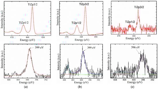
Figure 1.
High-resolution spectra for the Ti2p (top) and N1s (bottom) windows for samples (a) F01, (b) F02 and (c) F03, before sputtering.
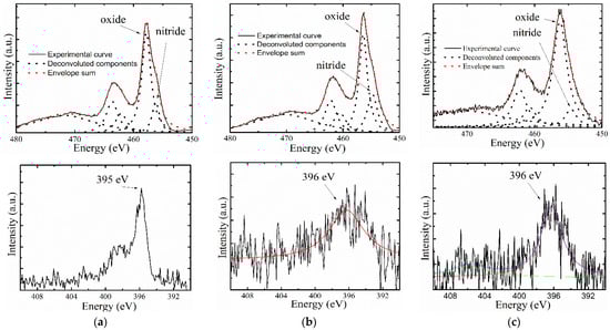
Figure 2.
High-resolution spectra for the Ti2p (top) and N1s (bottom) windows for samples (a) F01, (b) F02 and (c) F03 after sputtering.
In Figure 2, a convolution of oxide/nitride states, for the Ti2p transition, can be observed. In the figure, deconvoluted curves for both states are included. Oxide and nitride states are clearly differentiable, both in binding energy and in the shape of the transition. The shape of the Ti in the nitride state is modified because of the generation of satellites (caused by the extra conduction electrons) to the left of each transition, which produce asymmetry [11,14]. In Figure 1, a more symmetric shape in the Ti2p transition can be noted. Again, in Figure 2, the BE of Ti-oxide appears at 457–458 eV, while BE of Ti-nitride is about 1 eV lower, at 454–456 eV. This is expected, as the oxidized state tends to be more stable. The values of BE detected in our samples agree with the ones reported in the literature for oxide/nitride [12,13,15,16,17]. No oxy-nitride signal was detected in the Ti2p window, which is very distinguishable between the Ti-oxide and Ti-nitride and which appears at the middle in energy value [17,18]. In addition, metallic states of Ti were discarded. The assignation of the chemical states of samples was also supported by additional XPS analysis of the Ti and TiN targets, which are included in the Supplementary Materials.
From the area below the curve of the Ti2p3/2-nitride and N1s, and from using their respective sensitivity factors, the empirical formula for the nitride phase was obtained. Table 1 shows a summary of data obtained from the XPS analysis.

Table 1.
Summary of data obtained from XPS analysis. Second column is an account of the BE for each chemical state (eV). Third column is an account of the percentage of each chemical state. Last column is the obtained empirical formula. The analysis of F01, F02 and F03 corresponds to the substrates used as a template on which optical fibers were mounted.
From the XPS analysis, it is possible to conclude that the samples presented a mixture of coexisting phases of titanium nitride and titanium oxide. The most prevalent is the oxidized one. The nitride phase for samples F01 and F02 looks more metallic than for F03. It is possible that the higher deposition time favors the generation of more oxidation events.
The transmittance curves obtained from the UV–Vis measurements are included in Figure 3 for samples F01, F02 and F03, together with the Tauc curves at inset, and the n, k vs. λ of all samples in one graph. Figure 4 includes the transmittance curves for samples F0405 and F0607.
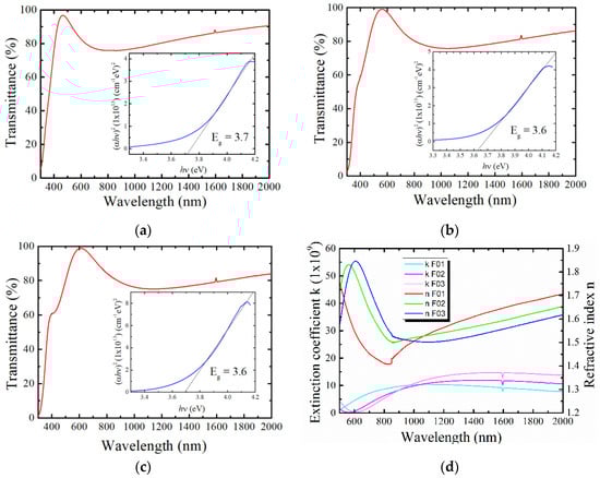
Figure 3.
Transmittance spectra for samples (a) F01, (b) F02 and (c) F03. Tauc curves are included in inset; (d) n and k vs. wavelength curves for the three samples.
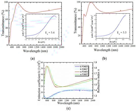
Figure 4.
Transmittance spectra for samples (a) F0405 and (b) F0607. Tauc curves are included in inset; (c) n and k vs. wavelength curves for the two samples.
The optical parameters were obtained from the transmittance spectra. Then, by the use of the Drude–Lorentz model, Eg, α, n and k were extracted. Applying the single-oscillator model developed by Wemple and Domenico, ε∞ (dielectric constant, real part, at high-frequency values, for electronic transitions) and ε0 (static constant, real part, at low-frequency values, related to the lattice contribution) were extracted [19]. A detailed procedure about how to use these models has been published by us elsewhere [20].
The TiN compound is formed from the hybridization of the orbitals Ti: 3d24s2 and N: 2p3. Thus, electronic levels are distributed in energy to conform the sp3d2 hybrid-orbital. Previous to hybridization, there are four and three valence electrons for Ti and N, respectively. When hybridization takes place, there is room for six electrons, and one remains free as a conductor electron. This final configuration is very similar to gold: 5d106s1. For this reason, TiN contains a high concentration of conduction electrons, ≈1022 cm−2, proportional to the conduction concentration of metallic elements, in this case to gold [7,10,15]. This metallic-like behavior for TiN can be observed in the transmittance spectra. The wavelength located at the onset, the region when transmittance starts to experiment a sudden drop, is defined as the screened plasma energy, λps, or the energy region where the real part of the dielectric constant ε∞ = 0. This wavelength, for metals such as gold and Ti nitrides, can be located within the visible spectral range and is affected by both intraband and interband characteristics (this is the cause of the yellowish color for both gold and stoichiometric TiN). At wavelengths λ < λps, it is also expected to produce a sharp rise in the refractive index, n, because of light attenuation due to the interband absorption, together with a reduction in transmittance and a maximum absorbance [7]. For regions λ > λps, an almost constant transmittance or transparent zone is expected. A drop in the transmittance is expected in the IR region at the onset of vibrational modes in the lattice [19,20].
At this region (transparent zone), a condition of high transmittance (low reflectance) is expected for typical semiconductors (SiO2, TiO2, sapphire). For metallic-like compounds, the transmittance depends on the density of the free carriers, which is influenced by the deposition conditions and film thickness. Thus, high reflectivity, similar to that of metals, coupled with low transmittance, may be possible.
In all the transmittance curves, the onset of the absorption edge is located at ~500–600 nm. This onset corresponds with wavelengths within the visible part of the spectra, and thus, all our films presented with a yellowish color, which is expected for TiN [21]. In this case, at this border, there are intraband transitions due to the interaction of light with the conduction electrons, which produce a maximum absorption at ≈λ = 600 nm. Between λ = 600 nm and λ = 800 nm, there is a transition zone. At λ = 800 nm, a transmittance of ≈80% is observed. Then, at the onset of the absorption edge, the absorption coefficient (a) can be calculated from the relation [18,19,20]:
where T is the measured transmittance, and d is the optical thickness. The optical band gap (Eg) was extracted from Tauc’s relation:
where A is the edge width parameter. The value of Eg is obtained by vs. with r = 2 for a direct transition, as reported for TiN [15,22]. In a direct transition, the maxima of density of states (DOS) at the top of valence level are aligned with the maxima of DOS at the bottom of the conduction level at k = 0 [20].
From the dispersion curve (n vs. λ), dielectric and static constants are obtained [19,20]. The procedure employed to extract the band gap from the Tauc’s curves is included in the Supplementary Materials.
In Table 2, a summary of the optical parameters extracted from the experimental transmittance curves is displayed.
Table 2.
Summary of optical parameters extracted from transmittance curves and applying the optical models. The analysis of F01, F02 and F03 corresponds to the substrates used as a template, where optical fibers were mounted. In addition, F0405 is the substrate used as a template, on which F04 and F05 were mounted (use of Ti target). Likewise, F0607 is the substrate used as a template, on which F06 and F07 were mounted (use of TiN target).
All films are similar in thickness, and the presented values for Eg range from 3.5 to 3.7 eV. These values agree for the titanium nitride films reported on by other authors, from 3.0 to 3.5 eV [15,21]. Values of Eg > 3.5 eV can be attributed to more metallic-like states, due to the non-stoichiometry of our films and the higher amount of loaded Ti, as the XPS analysis suggests. These additional electronic stats tend to be redistributed between the valence and conduction levels, giving place to band gap widening. In our case, the lowest value of the band gap at 3.4 eV corresponds to the film synthetized from the Ti target. Regarding the dielectric constants, the values were almost similar for all samples. The ε∞ has values in the range of Eg = 1.9–2.2 eV, where the value for F01 (synthesized from TiN target) is similar to F0405 (synthesized from Ti target). From these last values, we could observe that the optical properties using both synthesis routes would produce Ti nitride films with similar properties.
From Figure 3d and Figure 4c, “n” presents somewhat monovaluated stable values in the region of 1000–2000 nm, a transition region with an onset at ≈800 nm, with a sharp increase at 600 nm, which corresponds to the yellow region of the visible spectra, which is very distinguishable in the samples (see Figure S1c; Supplementary Materials).
From the data provided by XPS and UV–Vis characterization of the samples from the first batch and the UV–Vis characterization of samples from the second batch, we can conclude that the thin films of the non-stoichiometric TiN were synthesized. This films turned out to be metallic-rich, coexisting with a phase of titanium oxide.
2.3. Passive Q-Switched Laser Pulse Generation
For pulsing to occur, the SA accumulates a large amount of energy supplied by the pumping source, until saturation overflow is reached, leading to a release of energy in the form of a pulse of the order of microjoules. The experimental setup is a linear cavity laser containing an Er/Yb-doped double-clad fiber (EYDCF) with a length of ~1.2 m (DCF-EY-10/128, CorActive, Québec, QC, Canada), with a core absorption of 85 dB m−1 at 1535 nm and inner cladding absorption of 2 dB m−1 at 915 nm), which functions as a gain medium. The EYDCF pumps with a high-power 25 W laser at 976 nm, and the light beam passes through of a 2 × 1 + 1 combiner that allows for the passage of wavelengths at 976 and 1550 nm at the same time. On one side of the cavity is a fiber loop mirror (FLM) that consists of a 50/50 coupler with its output ports connected, which is used as a mirror capable of reflecting 100% of the incident light. At the other end is a 90/10 coupler from which the 10% output port was connected to an MBL fiber that is fixed horizontally to the base, with a flat mirror to the front. The 90% output port was the output of the laser signal and where the data measuring the pulsations were detected with the help of a photodetector, of which were read by means of an oscilloscope. Figure 5 shows the laser setup.
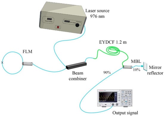
Figure 5.
Experimental setup of the PQS laser.
The laser pulses were detected with a photodetector and were recorded by an oscilloscope. Previously, test measurements were made with an MBL without deposited material to detect possible self-Q switches and to rule them out later, ensuring only to include the pulses generated by the nonlinear optical properties of the material. Table 3 is shown below, detailing the different MBLs that were used to perform the measurements.
Table 3.
MBL diameters for each sample measured.
The characteristics of the generated PQS laser pulses are shown in Figure 6, where it can be seen that all the samples maintain stability in the pump power range of 0.457 to 0.98 W, except in sample F03, in which unstable pulses were observed, attributed to the lack of available conduction electrons, since this sample had a lower amount of Ti (see Table 1). We think that this factor, and not the diameter of the optical fiber, explains this behavior.
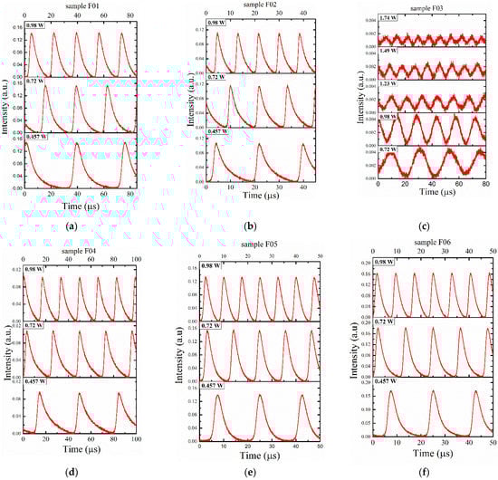
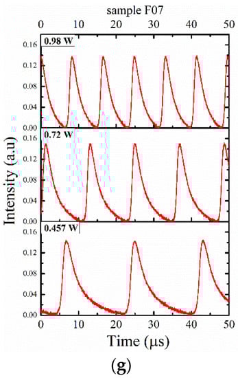
Figure 6.
Train of PQS pulses of the laser at different pump powers for the different MBL samples: (a) sample F01, (b) sample F02, (c) sample F03, (d) sample F04, (e) sample F05, (f) sample F06, (g) sample F07.
All the characteristics obtained from the information provided by the pulse trains are summarized in Table 4, while Figure 7 and Figure 8 appear in graphic form for each of the samples.
Table 4.
Characteristics of the PQS laser pulses generated in each of the samples while the pump power increases in a range of 0.57 to 0.98 W.
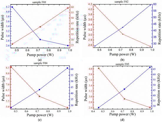
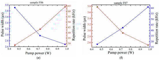
Figure 7.
Pulse width and repetition rate of the PQS pulses as a function of the pump power of MBL sample: (a) sample F01, (b) sample F02, (c) sample F04, (d) sample F05, (e) sample F06, (f) sample F07.
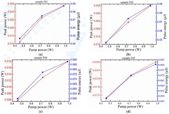
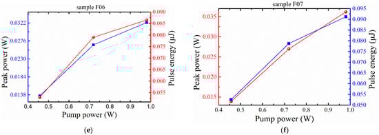
Figure 8.
Peak power and pulse energy of the PQS pulses as a function of the pump power of all MBL samples. (a) sample F01, (b) sample F02, (c) sample F04, (d) sample F05, (e) sample F06, (f) sample F07.
With this, it can be observed that the obtained laser pulses exhibit a typical behavior of PQS generation. By increasing the pump power, the repetition rate of the PQS pulses increases while the pulse width decreases.
From the figures, it can be shown that all the samples generate pulses at powers of 0.457, 0.72 and 0.98 W. These pulses are generated due to the material that covers each fiber. However, sample F03, in particular, presents alterations or modifications that are not detected in the others. Based on the data obtained from the analysis of the samples (XPS: see Table 1), it was observed that F03 presents a reduction in the amount of Ti when compared to the others (Ti0.4N0.6). It is possible that the reduction of the metal also reduces the amount of carriers that favor the interaction of the laser with the conduction electrons of the deposited material. In this way, it has been reported that the more metallic-rich the TiN phase, the better it is to sustain a pulsed laser operation by using the passive q-switching technique. Regarding the pulses in general, a similar and favorable response is observed in all the samples, regardless of the experimental conditions used in the RF deposition.
3. Deposition of Films by DC for LMR Refractometer Application
3.1. No-Core Fiber Structure and Deposition
The dielectric properties of the thin material film coated onto the optical fiber surface, which interacts with the light propagated through the fiber, are exploited in fiber sensors based on electromagnetic resonance responses, such surface plasmon resonance (SPR) and lossy mode resonance (LMR) phenomena. Instead of using a typical Kretschmann–Raether configuration for SPR and LMR bulky approaches, fiber structures effectively guide multiple modes supported by the fiber coating, with an angle greater than the attenuated total reflectance (ATR) angle, by total internal reflection (TIR). Then, with a significant phase coincidence between the guided light and the material coating, SPR and LMR occur in the optical fiber structures at the fiber-coating interface, where an evanescent wave is then produced. Depending on the wavelength of the light and the thickness of the material, mode coupling takes place when fiber-guided modes over the cut-off condition are guided through the material surface. As a result, energy is transferred from the light modes to a plasma wave generated at the interface surface at the resonance wavelength. Optically, the transferred energy generates a lack of intensity in the light through the fiber, which is detected as an intensity notch at the resonance wavelength in the output spectrum of the fiber transmission expressed by the power distribution of the input light source , the TIR critical angle , and the reflected light at the fiber–material interface , as [23]:
where stands for the number of reflections, depending on the coated fiber length L and the fiber diameter d.
In the case of SPR, electromagnetic resonance occurs at a single resonance wavelength; however, for LMR candidate materials, multiple resonant orders exist along a broadband wavelength range. Here, the exhibited plasmonic effect depends on the permittivity of the material coating and, as a consequence, on the complex refractive index conditions. LMR is obtained from materials on the low imaginary part of the refractive index. In this sense, different transition metal oxides (TMO) and metal nitrides have demonstrated to be good candidates to explore the LMR effect.
Moreover, in order to achieve generation of the LMR effect in optical fibers, it is necessary to ensure the strong interaction between the light guided through the fiber and the material deposited onto the fiber surface. For this purpose, different fiber structures such as chemically etched fibers, tapers, D-shaped fibers, and no-core fibers (NCF) have been studied for their application in fiber refractometers based on the LMR effect. In this case, although higher sensitivity properties on D-shaped fibers have been demonstrated, no-core fibers facilitate the implementation and deposition process, since special fiber preparation is not required. In our approach, NCF were used for the proposed application. The use of a multimode NCF eases the generation of strong evanescent waves from high-order modes excited from the fundamental mode propagated along the fiber surface. Figure 9 shows the fiber structure formed by an NCF segment spliced between two MMF segments. The proposed structure also facilitates the splicing process during the fabrication process due to fiber compatibility.
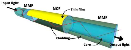
Figure 9.
No-core multimode fiber structure.
For the NCF deposition preparation, high vacuum tape and glass substrate were used for mounting and to fix the fiber structure. The film was deposited over the fiber surface as well as in the substrate. The film deposited in the substrate near the NCF was used for XPS characterization and optical thickness measurement. The same target (surface native oxide) was used to supply oxygen. A Filmetrics device in reflectance mode was used to measure the thickness of the films. From simulation analyses and from the results of our research group, it was demonstrated that for Ti compounds, film thickness from 200 to 300 nm allows for the generation of a strong second LMR order around 1500 nm [24]. For this purpose, DC magnetron sputtering from a TiN target was performed with a power of 250 W at 5 cm distance between the substrate and the target for 18 min. Oxygen was supplied from the same target (surface native oxide).
The deposition was made using a gas mixture containing argon (Ar) and nitrogen (N2), where Ar and N2 were the working and reactive gases, respectively. High purity (99.999%) Ar and N2 were employed for the TiOxNy deposition. The chamber was pumped down to a base pressure of 6.6 × 10⁻⁵ Torr before N2 and Ar were introduced. The flow rate of both gases was controlled during deposition by using gas flowmeters. The target-substrate distance d was fixed at 5 cm. A source from the DC Sputtering Ion Magnetron (Materials Science Inc., San Diego, CA, USA) was used during the deposition process. The pre-used vacuum evaporation was performed using two pumps: a mechanical JEOL75 G (Agilent, Santa Clara, CA, USA) and RP-250 Turbo Macrotorr turbomolecular V (Agilent, Santa Clara, CA, USA). The gas pressure was established using the flowmeter AERAFC-7800CD. After deposition, the thickness of the resulting film was measured ex situ by the Filmetrics equipment in reflectance mode. The measured film thickness was ~250 nm. A schematic diagram of the DC equipment used for the synthesis of this films is included in the Supplementary Materials.
Elemental characterization of the film was performed by the XPS equipment. A monochromatic AlKα source of 1486.68 eV was used to obtain the spectra. For the analysis, the binding energies were calibrated with the C1s peak at 284.5 eV. Figure 10 shows the XPS high-resolution spectra for Ti2p, O1s and N1s windows before and after sputtering.
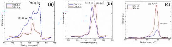
Figure 10.
XPS high-resolution spectra for sample 01 film for (a) Ti2p, (b) O1s and (c) N1s windows. The spectra before (b.s.) and after sputtering (a.s.) is presented.
The binding energies (BE) obtained from XPS spectra are presented in Table 5.
Table 5.
Binding energy values of the film.
For the Ti2p window shown in Figure 10a, before sputtering, the BE of Ti2p3/2 can be associated with a nonstoichiometric native oxide Ti oxide, as the metallic state is discarded. After sputtering, that Ti2p3/2 signal can be associated with an oxynitride phase. In addition, it a tendency of the BE to become lower can be observed, from 457.98 to 453.98 eV when Ti tends to nitridize. For the O1s window of Figure 10b, the BE before sputtering can also be related to native oxide. After sputtering, O1s can be related to an oxynitride phase. For the case of O1s, the BE before sputtering (531.5 eV) closely agrees with the reported value of the native oxide phase [25]. Conversely, this is not the case for the oxynitride phase, due to the wide variety of substoichiometric TiNxOy phases with different contents of O and N, which can turn into several variations in the chemical state and therefore into BE values. For N1s in Figure 10c, the BE change is not significant before and after sputtering. Thus, those signals can be related to the oxynitride phase. From the calculated atomic concentrations of Ti, N and O, extracted from the XPS spectra after sputtering, the empirical formula of the film was Ti0.37N0.41O0.21.
3.2. LMR Refractometer Results
In order to characterize the sensitivity of the fiber structure to refractive index variations of a liquid medium surrounding the coated fiber, the experimental setup of Figure 11 was used. The fiber structure was fixed between the holders of a mechanical device, and then, the NCF was immersed in liquid solutions from a set with different refractive indices. A broadband NIR LED source with emissions in the range of 1400 to 1700 nm was used as the input light source. The transmitted optical spectrum was measured to determine the characteristics of the output light by using a NIR spectrometer with a wavelength range from 970 to 1700 nm.
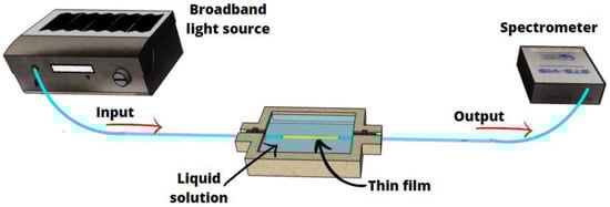
Figure 11.
Experimental setup for LMR refractometer.
The measurements of the output transmitted signal and the transmission of the coated fiber are shown in Figure 12. The spectrum of the input light source (black line) was directly obtained with the source connected to the spectrometer. As can be observed, the spectrum of the broadband source spans from ~1400 to ~1650 nm. The spectrum of the transmitted light through the fiber (red line) exhibits a transmission notch at 1512.3 nm. The inset of Figure 12 shows the transmission calculated as the division of the transmitted signal over the input light signal, shown in dBm units. The results were obtained for the NCF structure submerged in a solution with a refractive index of 1.36. The observed transmission notch corresponds to the second LMR order, which exhibits a depth of ~6 dB.
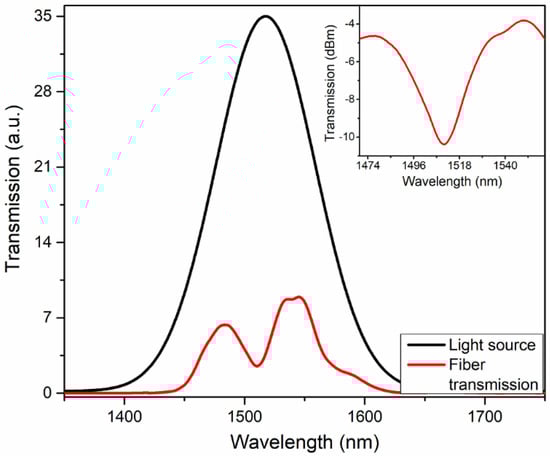
Figure 12.
Output spectrum and transmission of the fiber structure.
The characterization of the wavelength displacement of the transmission notch as a function of the variations on the refractive index of the liquid medium surrounding the coated fiber is shown in Figure 13. As can be observed, with the increase in the refractive index of the surrounding medium, the transmission notch displaces toward longer wavelengths as the depth of the notch decreases.
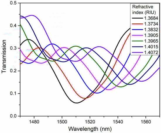
Figure 13.
Wavelength displacement of the transmission notch as a function of the refractive index variations.
From the results obtained in Figure 13, the characteristic curve of the refractometer is obtained by wavelength displacement interrogation, as shown in Figure 14. As it can be observed, the results can be fitted to a linear function with R2 of 0.996. The sensitivity, obtained from the slope, is 1184.91 nm/RIU in a refractive index ranging from 1.3684 to 1.4072.
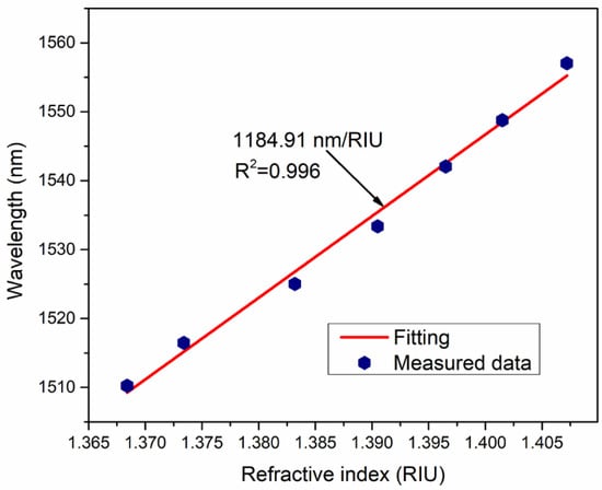
Figure 14.
Wavelength displacement of the transmission notch as a function of RI variation wavelength shift sensitivity.
4. Conclusions
Titanium nitride thin films were synthesized by the technique of RF reactive magnetron sputtering. The thin films were deposited on a glass substrate, on which optical fibers were placed. After deposition, the substrates were characterized by means of XPS and UV–Vis spectroscopy. The analysis showed the formation of oxide and nitride phases, where the TiN phase was non-stoichiometric and metal-rich. The forbidden width of the nitride phase presented values in the range of Eg = 3.4–3.7 eV. The coated fibers were then placed in a Q-switch laser optical system, with the purpose of detecting and characterizing the plasmonic response at an energy region of around 1.55 μm. Regular pulses were detected in the region close to the output energy of the laser, which was generated by the interaction of light with the plasmonic modes of the thin film.
Finally, we report the applications as a saturable absorber and LMR fiber refractometer of different fiber structures coated with thin films of titanium nitride compounds deposited by DC/RF magnetron sputtering. The obtained results demonstrate the reliability of the sputtering technique to equalize the deposition parameters in order to obtain specific optical properties for the proposed applications.
Supplementary Materials
The following supporting information can be downloaded at: https://www.mdpi.com/article/10.3390/coatings13010095/s1, Figure S1: (a) Sputtering system for RF deposition (b) Schematic detail of the deposition chamber; Figure S2: Sputtering system for DC deposition; Figure S3: Tauc´s curve with the procedure used to obtain Eg; Figure S4: (a) Ti target (b) TiN target; Figure S5: XPS spectra for the Ti2p and N1s high resolution windows for TiN target; Figure S6: XPS spectra for the Ti2p and N1s high resolution windows for Ti target.
Author Contributions
R.I.Á.T. and M.G.M. conceived and designed the experiments; M.G.M., P.P.C. and O.G.R. contributed to the sputtering deposition and thin-film characterization by XPS; R.I.Á.T. and O.G.R. performed the experiments of the PQS laser; P.P.C. and R.I.Á.T. performed the experiments of the LMR refractometer; M.G.M. and R.I.Á.T. contributed the reagents, materials, and analysis tools; O.G.R., P.P.C., R.I.Á.T. and M.G.M. wrote, reviewed, and edited the paper. All authors have read and agreed to the published version of the manuscript.
Funding
This research was funded in part by Universidad Autónoma de Nuevo León: 245-CE-2022; Universidad Popular Autónoma del Estado de Puebla: Fondo de investigación UPAEP 2022.
Institutional Review Board Statement
Not applicable.
Informed Consent Statement
Not applicable.
Data Availability Statement
Not applicable.
Acknowledgments
This work was supported by the PAICyT UANL project under grant 245-CE-2022. Omar Gaspar Ramírez is thankful for CONACyT Posgraduate scholarship grant 817293.
Conflicts of Interest
The authors declare no conflict of interest.
References
- Ponja, S.D.; Williamson, B.A.; Sathasivam, S.; Scanlon, D.O.; Parkin, I.P.; Carmalt, C.J. Enhanced electrical properties of antimony doped tin oxide thin films deposited via aerosol assisted chemical vapour deposition. J. Mater. Chem. C 2018, 6, 7257–7266. [Google Scholar] [CrossRef]
- Mohammed, M.A.; Salman, S.R.; Wasna’a, M.A. Structural, optical, electrical and gas sensor properties of ZrO2 thin films prepared by sol-gel technique. NeuroQuantology 2020, 18, 22. [Google Scholar] [CrossRef]
- Ashok, A.; Regmi, G.; Romero, N.A.; Solis, L.M.; Velumani, S.; Castaneda, H. Comparative studies of CdS thin films by chemical bath deposition techniques as a buffer layer for solar cell applications. J. Mater. Sci. Mater. Electron. 2020, 31, 7499–7518. [Google Scholar] [CrossRef]
- Ricardo, I.Á.T.; Omar, G.R.; Patricia, P.C.; Manuel, G.M.; Antonio, B.P. TiOxNy Thin Film Sputtered on a Fiber Ball Lens as Saturable Absorber for Passive Q-Switched Generation of a Single-Tunable/Dual-Wavelength Er-Yb Double Clad Fiber Laser. Nanomaterials 2020, 10, 923. [Google Scholar]
- Nikhil, K.P.; Daniel, J.R.A.; Erhan, A.; King, P.J.; Srinivas, G.; Kelvin, S.K.K.; Anthony, O.N. Effect of deposition conditions and post deposition anneal on reactively sputtered titanium nitride thin films. Thin Solid Film 2015, 578, 31–37. [Google Scholar]
- Swann, S. Magnetron sputtering. Phys. Technol. 1988, 19, 67. [Google Scholar] [CrossRef]
- Jarosław, J.; Piotr, W.; Paweł, P.M.; Monika, O.; Bartłomiej, W.; Aleksandra, S.; Michał, S.; Cezariusz, J.; Krzysztof, Z. Titanium Nitride as a Plasmonic Material from Near-Ultraviolet to Very-Long-Wavelength Infrared Range. Materials 2021, 14, 7095. [Google Scholar]
- Luca, M.; Tapan, B.; Beatrice, R.B.; Filip, M.; Andrea, L.B.; Stepan, K.; Alberto, N. Controlling the plasmonic properties of titanium nitride thin films by radiofrequency substrate biasing in magnetron sputtering. Appl. Surf. Sci. 2021, 554, 149543. [Google Scholar]
- Chun, C.C.; John, N.; Yang, Z.P.; Wilton, J.M.K.-P.; Willard, R.; Ting, S.L.; Diego, A.R.D.; Abul, K.A.; Hou-Tong, C. Highly Plasmonic Titanium Nitride by Room-Temperature Sputtering. Sci. Rep. 2019, 9, 15287. [Google Scholar]
- Gururaj, V.N.; Jeremy, L.S.; Xingjie, N.; Alexander, V.K.; Timothy, D.S.; Alexandra, B. Titanium nitride as a plasmonic material for visible and near-infrared wavelengths. Optical Materials Express 2012, 2, 478–489. [Google Scholar]
- Jiachang, B.; Ruyi, Z.; Shaoqin, P.; Jie, S.; Xinming, W.; Wei, C.; Liang, W.; Junhua, G.; Hongtao, C.; Yanwei, C. Robust plasmonic properties of epitaxial TiN films on highly lattice-mismatched complex oxides. Physical Review Materials 2021, 5, 075201. [Google Scholar]
- Barhai, P.K.; Neelam, K.; Banerjee, I.; Pabi, S.K.; Mahapatra, S.K. Study of the effect of plasma current density on the formation of titanium nitride and titanium oxynitride thin films prepared by reactive DC magnetron sputtering. Vacuum 2010, 84, 896–901. [Google Scholar] [CrossRef]
- White, N.; Campbell, A.L.; Grant, J.T.; Pachter, R.; Eyink, K.; Jakubiak, R.; Martinez, G.; Ramana, C.V. Surface/interface analysis and optical properties of RF sputter-deposited nanocrystalline titanium nitride thin films. Appl. Surf. Sci. 2014, 292, 74–85. [Google Scholar] [CrossRef]
- Available online: https://www.thermofisher.com/mx/es/home/materials-science/learning-center/periodic-table.html (accessed on 13 November 2022).
- Solovana, M.N.; Brusa, V.V.; Maistruka, E.V.; Maryanchuk, P.D. Electrical and Optical Properties of TiN Thin Films. Inorg. Mater. 2014, 50, 40–45. [Google Scholar] [CrossRef]
- Van Bui, H.; Groenland, A.W.; Aarnink, A.A.I.; Wolters, R.A.M.; Schmitz, J.; Kovalgin, A.Y. Growth kinetics and oxidation mechanism of ALD TiN thin films monitored by in situ spectroscopic ellipsometry. J. Electrochem. Soc. 2011, 158, H214–H220. [Google Scholar] [CrossRef]
- Saha, N.C.; Tompkins, H.G. Titanium nitride oxidation chemistry: An x-ray photoelectron spectroscopy study. J. Appl. Phys. 1992, 72, 3072–3079. [Google Scholar] [CrossRef]
- Solis Pomar, F.; Nápoles, O.; Vázquez Rbaina, O.; Gutierrez Lazos, C.; Fundora, A.; Colin, A.; Pérez Tijerina, E.; Melendrez, M.F. Preparation and characterization of nanostructured titanium nitride thin films at room temperature. Ceram. Int. 2016, 42, 7571–7575. [Google Scholar] [CrossRef]
- Wemple, S.H.; DiDomenico Jr, M. Behavior of the electronic dielectric constant in covalent and ionic materials. Phys. Rev. B 1971, 3, 1338–1351. [Google Scholar] [CrossRef]
- Manuel, G.M.; Alvaro, B.C.; Ricardo, R.S.; Víctor, C. Investigation of the annealing effects on the structural and opto-electronical properties of RF-sputtered ZnO films studied by the Drude-Lorentz model. Appl. Phys. A 2015, 120, 1375–1382. [Google Scholar]
- Arnaud, V.; Maria Alejandra, U.H.; Gaylord, G.; Nicolas, C.M.; Damien, J.; Marion, H.; Jean, Y.M.; Stéphanie, R.; Francis, V.; Carmen, J.; et al. Optical, electrical and mechanical properties of TiN thin film obtained from a TiO2 sol-gel coating and rapid thermal nitridation. Surf. Coat. Technol. 2021, 413, 127089. [Google Scholar]
- Hengyong, W.; Mingming, W.; Zhanliang, D.; Ying, C.; Jinglong, B.; Jian, L.; Yun, Y.; Yingna, W.; Yi, C.R.W. Composition, microstructure and SERS properties of titanium nitride thin film prepared via nitridation of sol–gel derived titania thin films. J. Or Raman Spectrosc. 2017, 48, 578–585. [Google Scholar]
- Dwivedi, Y.S.; Sharma, A.K.; Gupta, B.D. Influence of skew rays on the sensitivity and signal-to-noise ratio of a fiber-optic surface-plasmon-resonance sensor: A theoretical study. Appl. Opt. 2007, 46, 4563–4569. [Google Scholar] [CrossRef] [PubMed]
- Ricardo Iván, Á.T.; Patricia, P.C.; Manuel, G.M.; Abel, F.C. Lossy mode resonance refractometer operating in the 1.55 µm waveband based on TiOxNy thin films deposited onto no-core multimode fiber by DC magnetron sputtering. Opt. Fiber Technol. 2022, 71, 102929. [Google Scholar]
- Lubinda, L. Debate over Mapostori use of open spaces. Harare News 2015, 16, 10–17. [Google Scholar]


Disclaimer/Publisher’s Note: The statements, opinions and data contained in all publications are solely those of the individual author(s) and contributor(s) and not of MDPI and/or the editor(s). MDPI and/or the editor(s) disclaim responsibility for any injury to people or property resulting from any ideas, methods, instructions or products referred to in the content. |
© 2023 by the authors. Licensee MDPI, Basel, Switzerland. This article is an open access article distributed under the terms and conditions of the Creative Commons Attribution (CC BY) license (https://creativecommons.org/licenses/by/4.0/).