Article

Tailoring Mechanical Properties of a-C:H:Cr Coatings

1
Laboratoire d’Analyse par Réaction Nucléaires (LARN), Namur Institute of Structured Matter (NISM), University of Namur, 61 Rue de Bruxelles, 5000 Namur, Belgium
2
Institute of Mechanics, Materials and Civil Engineering (iMMC), Université catholique de Louvain, av G Lemaître 4, 1348 Louvain-la-Neuve, Belgium
3
Univ. Lyon, Mines Saint Etienne, CNRS UMR 5307 LGF, Centre SMS, 42100 Saint Etienne, France
4
Electron Microscopy for Materials Science (EMAT), University of Antwerp, Groenenborgerlaan 171, 2020 Antwerp, Belgium
5
WEL Research Institute, Avenue Pasteur, 6, 1300 Wavre, Belgium
*
Author to whom correspondence should be addressed.
Coatings 2023, 13(12), 2084; https://doi.org/10.3390/coatings13122084
Submission received: 21 November 2023 / Revised: 4 December 2023 / Accepted: 7 December 2023 / Published: 14 December 2023
(This article belongs to the Section Plasma Coatings, Surfaces & Interfaces)

Abstract

:
The development of coatings with tunable performances is critical to meet a wide range of technological applications each one with different requirements. Using the plasma-enhanced chemical vapor deposition (PECVD) process, scientists can create hydrogenated amorphous carbon coatings doped with metal (a-C:H:Me) with a broad range of mechanical properties, varying from those resembling polymers to ones resembling diamond. These diverse properties, without clear relations between the different families, make the material selection and optimization difficult but also very rich. An innovative approach is proposed here based on projected performance indices related to fracture energy, strength, and stiffness in order to classify and optimize a-C:H:Me coatings. Four different a-C:H:Cr coatings deposited by PECVD with Ar/C2H2 discharge under different bias voltage and pressures are investigated. A path is found to produce coatings with a selective critical energy release rate between 5–125 J/m2 without compromising yield strength (1.6–2.7 GPa) and elastic limit (≈0.05). Finally, fine-tuned coatings are categorized to meet desired applications under different testing conditions.

Graphical Abstract

1. Introduction

Amorphous carbon (a-C) coatings have been extensively studied for their outstanding mechanical [1,2], chemical [3], and biological properties [4]. These coatings, deposited by vacuum technology, have shown tunable properties such as high hardness, low friction, and acceptable wear resistance. However, variations in coating properties, poor adhesion, thickness uniformity, and environmental stability remain challenging [5].
Plasma-Enhanced Chemical Vapor Deposition (PECVD) allows for tuning coatings’ physical and chemical properties by varying deposition parameters, such as pressure and gas composition. In addition, the chemical structure is affected by the magnitude of the impinging energy of the ions [6]. Acetylene (C2H2) is often used for a-C:H deposition due to its high electron-molecule cross-section and high deposition rate [7,8].
Adding metal elements to the coatings can decrease internal stress and improve wear resistance, adhesion, thermal stability, and fracture toughness [9,10]. The rise in sp2 graphitization by doping metal elements and partly hard carbide phase dispersion in amorphous carbon explains this phenomenon [11]. Among many metallic elements, chromium (Cr), in combination with carbon, presents attractive mechanical properties (exceptionally stable friction performance and toughness) in a-C coatings [12,13,14].
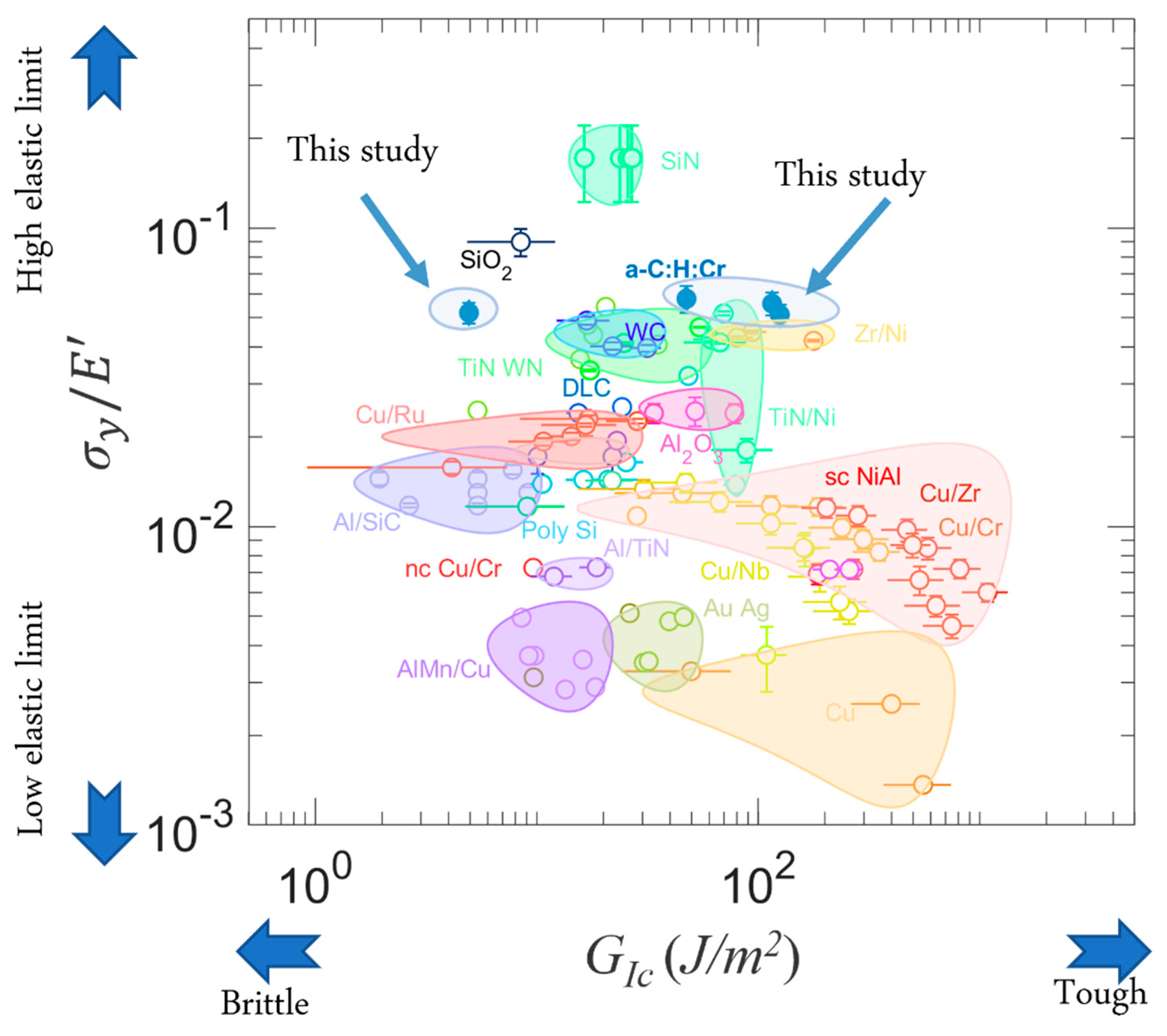
The aim of this research is to understand further how the deposition parameters affect the mechanical characteristics (both effective and intrinsic) of thin a-C:H:Cr coatings with thickness in the 1 μm range to build a rational coating selection strategy to optimize the systems further. To this end, we capitalized on the previous work by our group [15,16] to demonstrate how a-C:H:Cr coatings can be produced with tailored mechanical properties, specifically strength and fracture toughness by varying only the deposition conditions in C2H2 magnetron-assisted discharge. Because of the ionic nature of the condensing species in such a setup, one can easily understand that substrate biasing is one of the methods to produce coatings with different properties, as well as traditional pressure variation. Four coatings have been selected as representative candidates for this study and characterized by comprehensive techniques, including X-ray Photoelectron Spectroscopy (XPS) to extract the coating’s chemical composition; Atomic Force Microscopy (AFM) and Scanning Electron Microscopy (SEM) to observe the structural and morphological properties of the coatings; Transmission Electron Microscopy (TEM) and X-ray diffractometer (XRD) to investigate the amorphous microstructure of the coating; Raman Spectroscopy to track structural variation; nanoindentation to determine the hardness, Young’s modulus, and activation volume; micro-scratch test to extract wear resistance, critical load, as well as tensile tests on a supporting polymer membrane to determine the fracture toughness of the coating. Comparison and deeper discussion are made through analyzing materials property map presenting the ratio of yield strength over Young’s modulus ( σ y E ) against critical fracture energy release rate (   G I c ) for several materials. The performances are shown to position extremely well compared to other available coatings for various applications asking for high-yielding strength, high critical load under scratching conditions, and elastic limit, with a wide range of critical energy release rates.

2. Materials and Methods

2.1. Coating Deposition

The a-C:H:Cr coatings with 10 at% of Cr and around 30 at% of hydrogen content were deposited on {100} silicon wafers, on 13 µm and 25 µm thick HN type Kapton substrates by means of PECVD magnetron sputtering [15,16]. Silicon substrates were ultrasonically cleaned in soap and de-ionized water and dried with hot air prior to the deposition. The polymer substrates were used as received by the supplier. A base pressure of 10−4 Pa was created prior to the deposition to remove contamination. Then, a 10 min Cr target cleaning with 1.2 kW power was performed under a pure Ar atmosphere. Cr targets (7.5 × 35 cm, purity 99.8%, Nova Fabrica) have been sputtered in argon and acetylene (C2H2) mixed atmosphere (150 sccm Ar/160 sccm C2H2) under different deposition conditions (0.66 Pa, 2.66 Pa sputtering pressure, floating or −100 V bias voltage). The gas flow rate was controlled by FloTron multi-channel reactive gas monitoring system. A bipolar pulsed power supply working with a frequency of 1250 Hz and a pulse duration of 300 µs on and 100 µs off was used (duty cycle of 75%). Three-fold sample rotation around the Z axis along with 2 rpm table rotation speed has been applied in order to generate homogeneous coating. The deposition was conducted at room temperature. The coating thickness was set at around 1 µm, i.e., sufficiently thick to perform the relevant mechanical tests. Figure 1 schematically illustrates a cross-section of the semi-industrial chamber of about one cubic meter from D&M Vacuumsystemen.

2.2. Characterization of the Coatings

2.2.1. Chemical and Structural Analysis

The structural properties and phase purity of a-C:H:Cr coatings were explored by XRD using PANalytical X’Pert PRO diffractometer (Malvern Panalytical, Malvern, UK) in the 2 θ - ω configuration to remove the background caused by the silicon substrate. The angle between the incident X-ray beam and the detector forms an angle of 2 θ , and the ω angle represents the angle at which the X-ray beam hits the sample. Monochromatic Cu k α Wavelength λ = 0.15406 nm has been used as the X-ray source. The device has been operated at 45 kV and 30 mA.
The microstructure of the a-C:H:Cr samples has been determined by TEM including selected area electron diffraction (SAED), high-resolution transmission electron microscopy (HRTEM), and energy dispersive X-ray spectroscopy (EDXS) on Thermo Fisher Tecnai (Thermo Scientific, Waltham, MA, USA) Osiris microscope operated at 200 kV.
The composition depth profile of the a-C:H:Cr coatings has been determined by X-ray photoelectron spectroscopy (XPS) depth profiling using a monochromatic X-ray source (Al Kα radiation 1486.6 eV, spot size of 250 × 250 µm) using Ar+ with an energy of 2 keV scanning over an area of 1.25 mm × 1.25 mm with incident angle of 30°, on ThermoFisher K-alpha spectrometer (Thermo Scientific, Waltham, MA, USA). The chamber pressure before the acquisition was below 9.9 × 10⁻⁷ Pa. Each level of O 1s, Cr 2p, C 1s, and Si 2p (for substrate) is collected using snap mode (pass energy 147 eV, 10 snaps), with an erosion rate of 0.45 nm/s. The concentration is derived from each level, considering a Shirley background. A flood gun has been used during analysis, preventing eventual charging effects. No further energy shift is applied to the signal. The authors are aware of the recent warnings about XPS analysis [17,18]. Here, only the area of the peaks is considered, eventual energy shifts are not problematic. Approximately 30 at% of hydrogen was detected in each sample by the Elastic Recoil Detection technique (ERD) which is not considered in XPS data. All XPS data are computed using Avantage v.5.9916 Build 06625 software.
Raman spectroscopy was used to examine the structural variation of a-C:H:Cr coatings. The backscattering configuration using a LabRam HR 800 confocal laser system (Horiba, Kyoto, Japan) was selected with a laser wavelength λ = 514 nm and a 2400 gr/mm grating. The spectral resolution for this configuration is ≈0.5 cm−1. In order to avoid local heating and allow accurate measurement, the laser power was set to 10% of the maximum working power. All measurements were made without any polarization.
AFM measurements were performed in air, using the soft tapping mode of a Nanoscope III from Veeco Instruments (Santa Barbara, CA, USA). Images were recorded in 4 × 4 µm2, and 2 × 2 µm2 sizes with 512 × 512 lines per image and a scan rate of 1 Hz. The silicon cantilever (Nanosensors PPP-NCHR, Nanosensors, Redwood City, CA, USA) with a resonance frequency of 290 kHz and a typical spring constant of around 42 N/m has been used for analysis. The tip has a nominal radius lower than 10 nm. The ratio between the set-point amplitude and the free amplitude of the cantilever vibration was always kept above 0.8. The average of three measurements for each sample has systematically been used. The topographic analysis of AFM images of the surface roughness was carried out using the Gwyddion software version 2.59.
The coating thickness, surface morphology, and cross-sectional growth were determined using a ZEISS Ultra 55 Field Emission Gun–Scanning Electron Microscope (FEG-SEM, Zeiss, Oberkoche, Germany). An electron high tension (EHT) of 5 kV in in-lens and secondary electron (SE) modes has been used to generate clear and less electrostatically distorted nano-structures images.

2.2.2. Nanoindentation and Micro-Scratch Tests

The hardness, Young’s modulus, and apparent activation volume have been determined by nanoindentation using a G200 nanoindenter (KLA Tencor, KLA, Milpitas, CA, USA equipped with the Dynamic Contact Module (DCM) II head with 50 nN and 0.01 nm of force and vertical displacement resolution, respectively. A diamond Berkovich tip has been used and the tip area function has been calibrated using a fused silica reference. The nanoindentation measurements were performed at room temperature, under the load-control mode, with an exponential loading in order to produce a constant strain rate of P ˙ / P = 0.05 s−1. The thermal drift rate has been limited to 0.05 nm s−1 before each experiment to ensure a negligible impact on the measured displacement. Sixteen indents were made within each sample for statistical analysis and consistency inspection. The measurements were carried out using the continuous stiffness measurement (CSM) technique providing continuous hardness and Young’s modulus with increasing indentation depth. The hardness and modulus were calculated using the Oliver and Pharr model [19]. Also, Young’s modulus of the coating was corrected from the substrate effect using the model proposed by Hay and Crawford [20]. In order to extract the apparent activation volume, constant contact stiffness relaxation tests have been performed with a holding duration of 30 min and a maximum penetration depth of 90 nm. According to Gu et al. [21], the activation volume V* is extracted from nano-indentation as follows:
V * = 3 3 k T l n ε ˙ i H ,
where ε ˙ i stands for the indentation strain rate, k represents Boltzmann’s constant, and T is the testing temperature. The corresponding experimental and data processing procedures are explained in more detail in [22].
Micro-scratch experiments were performed using a G200 nanoindenter (KLA Tencor) with a XP head equipped with a lateral force measurement. This setup allows the measurement of the coefficient of friction during scratch. The XP head has a maximum normal force of 500 mN. A sphero-conical diamond tip with a radius of 5 µm and 90 degrees cone equivalent angle was used to perform the tests. Experiments involve applying a linear axial loading from 0 to 100 mN while sliding the indenter tip over 600 µm with a velocity of 30 µm·s−1. The sample surface along the scratch path was scanned at low load (20 µN) with the indenter tip before and after the experiment to characterize the surface roughness and topology before, and measure the residual profile afterward. For each sample, a set of 8 scratches has been performed. Scratch grooves were observed by SEM to characterize the failure mechanisms along the wear track.

2.2.3. Tensile Test on Polymer Substrate

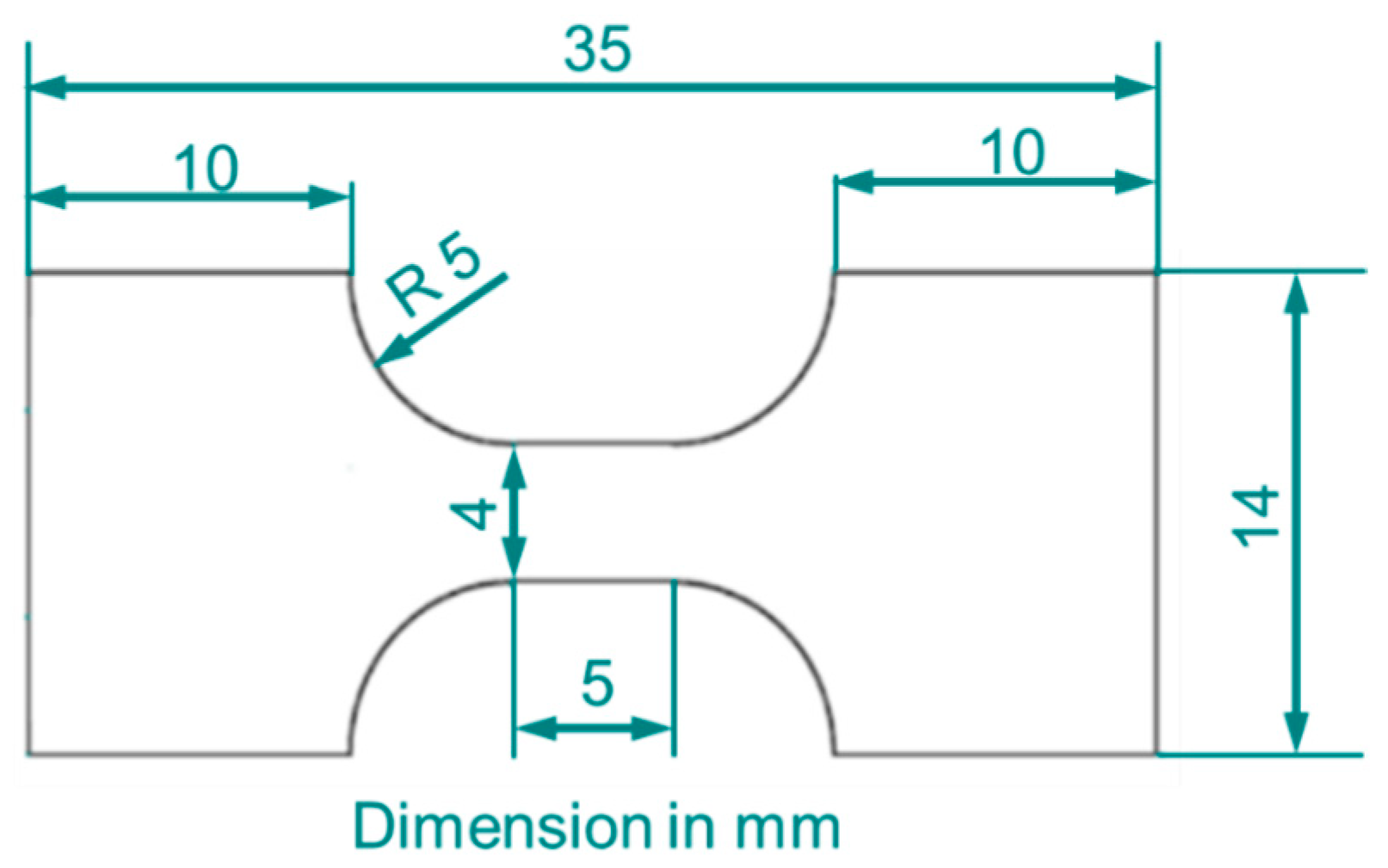
The fracture toughness of a-C:H:Cr coatings has been determined by deforming the coatings deposited on polymer substrates up to cracking. Prior to coating deposition, the polymer sheet was cut into tensile specimens using a punch. The geometry of the specimens is shown in Figure 2. In-situ optical microscope and in-situ SEM tensile tests were performed with a Gatan micro testing machine with a maximum force of 2 kN and displacement rate of 0.1 mm/min. All experiments were performed at room temperature.
The cracking behavior was characterized in-situ by SEM, while in-situ optical microscope tensile tests were used to characterize the fracture toughness of the coatings. In-situ SEM tests require interrupting the test for imaging, which leads to some spurious creep in the polymer substrate. It has been shown in the literature that test interruption can lead to crack propagation even when the mode I stress intensity factor (KI) remains below the critical value (KIc) of the coating [23]. Meanwhile, in-situ SEM tensile tests have been used to accurately determine the saturation crack density ( ρ s c ), i.e., the maximum crack density reached when pulling on the specimen. In-situ SEM tests were initially stopped every 50 µm of crosshead displacement until 400 µm in order to take images at various magnifications. After the first 400 µm of displacement, the experiment was stopped every 100 µm of displacement until a total crosshead displacement of 1 mm. Two images per second were acquired during in-situ optical microscope tensile test at a magnification of 200× with a resolution of 1272 × 952 pixels which ensures looking at the whole specimen gauge length while seeing the cracks. These parameters are well suited to observe crack propagation and calculate the critical fracture energy release rate G I c from
G I c = Z σ f 2 h f E f   ,
where Z is a dimensionless parameter that depends on the elastic mismatch between the coating and substrate, σ f is the fracture stress in the coating, hf is the coating thickness and E f = E f / ( 1 ν 2 ) is the plane strain of Young’s modulus. The Z factor depends on the Dundurs parameter α as defined in [24] and on the substrate/coating thickness ratio [25]. The stress inside the coating is obtained from Young’s modulus and from the strain at which the first crack is propagating, assuming the coating behaves as a linear elastic material and using Young’s modulus extracted by nanoindentation. This will turn out to be a reasonable hypothesis with respect to the level of strain that is reached when looking at the literature [26,27]. The fracture strain ( ε f ) is measured by following the displacement of small asperities on the images located close to the end of the gage region of the specimen. Note that the residual stress of a-C:H:Cr is considered equal to zero because the soft polymer substrate rapidly relaxes this stress, contrary to the condition impressed by a Si substrate. Finally, Equation (2) can be rewritten as
G I c = Z h f E f ε f 2 ,
and the related stress intensity factor KIc as
K I c = G I c E f   ,
Despite the possibility of extremely high fracture toughness, the relatively high yield strength causes a reduction in the size of the fracture process zone, d, ahead of the crack tip [28]. The fracture process zone size, d, is defined as
d = K I c 2 π σ y 2   ,
where σ y is the yield strength of the coating.

3. Results

3.1. Structure, Composition and Surface Morphology

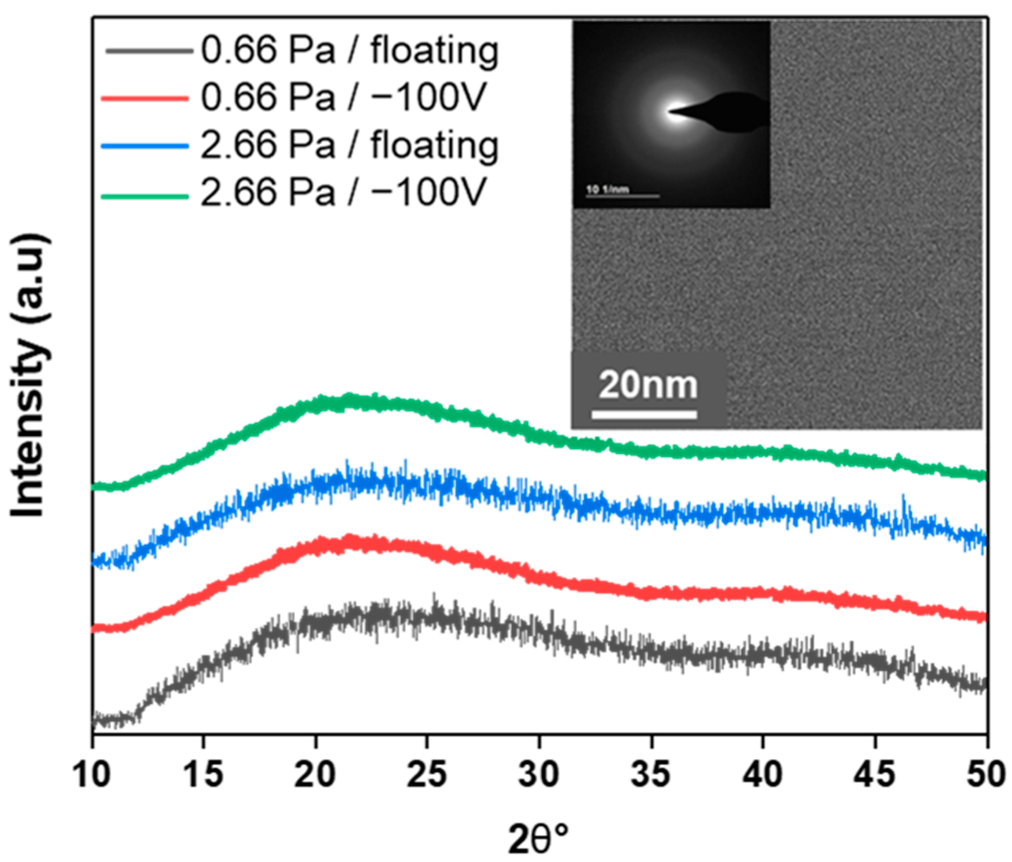
The microstructure of the a-C:H:Cr coatings under different deposition conditions (0.66 Pa, 2.66 Pa sputtering pressure, floating or −100 V bias voltage) have been studied by XRD and TEM analysis. X-ray diffractograms of the coatings detected no crystallinity in the coatings showing a fully amorphous nature of the coatings. The high-resolution micrograph and SAED pattern from TEM also confirm the amorphous character of the deposited coatings (see Figure 3).
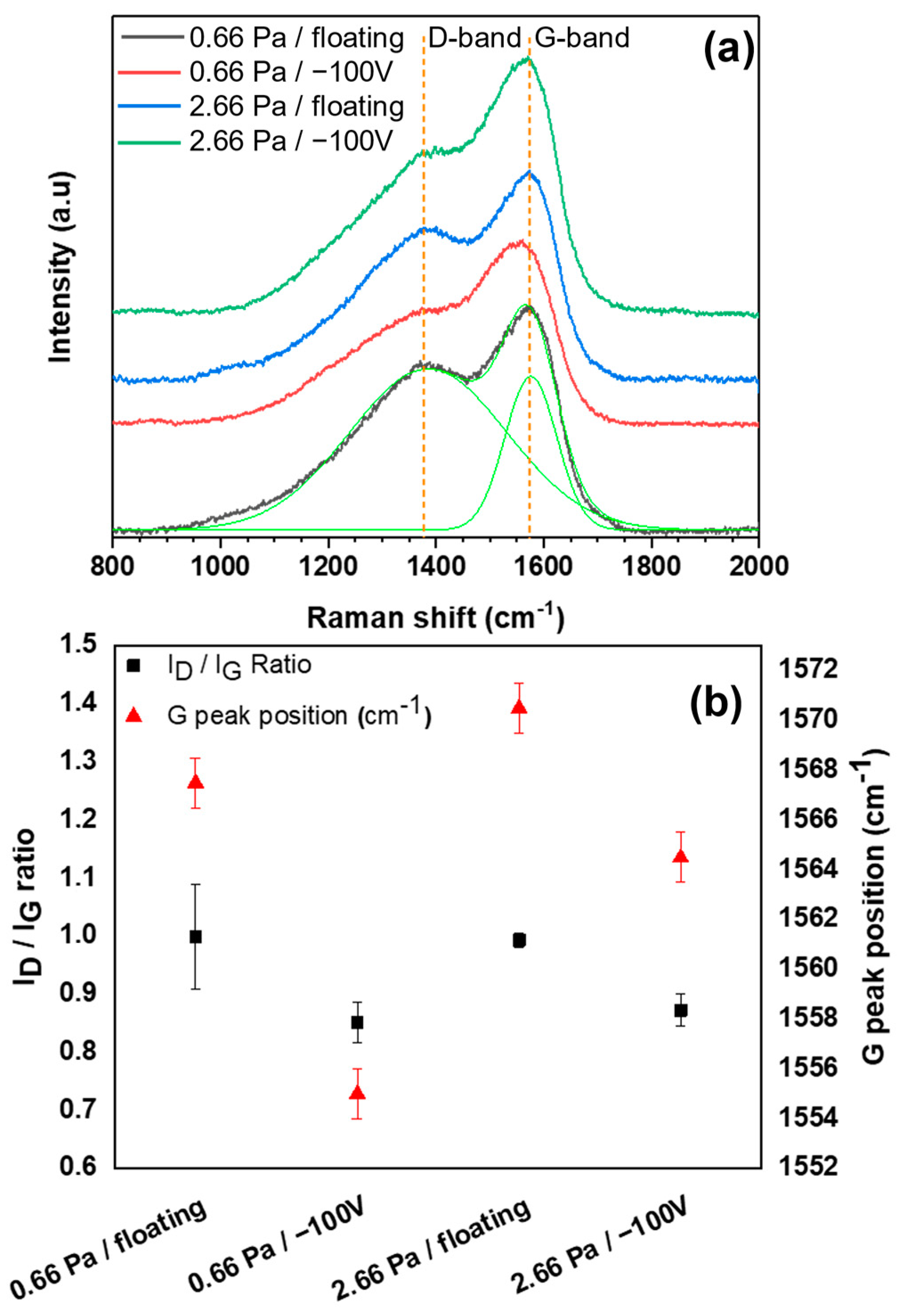
Figure 4 displays the Raman spectra of the coatings. Each Raman spectrum was fitted into two Gaussian peaks. When applying a bias voltage, a small shift to the lower wave number is observed in the positions of the G peak (≈12 cm−1 and ≈6 cm−1 for 0.66 Pa and 2.66 Pa, respectively). Also, an increase in FWHM of the G peak (from ≈112 to ≈130 cm−1 and ≈110 to ≈122 cm−1 for 0.66 Pa and 2.66 Pa, respectively), and D peak (from ≈334 to ≈339 cm−1 and ≈328 to ≈334 cm−1 for 0.66 Pa and 2.66 Pa, respectively), have been observed with the bias voltage application which is an indicator of more disordered amorphous coating. A decrease in the ratio of the D-band intensity to that of the G-band (ID/IG) and the G-band position are both indicators of lower hydrogen content and a rising sp3 content, respectively [29,30].
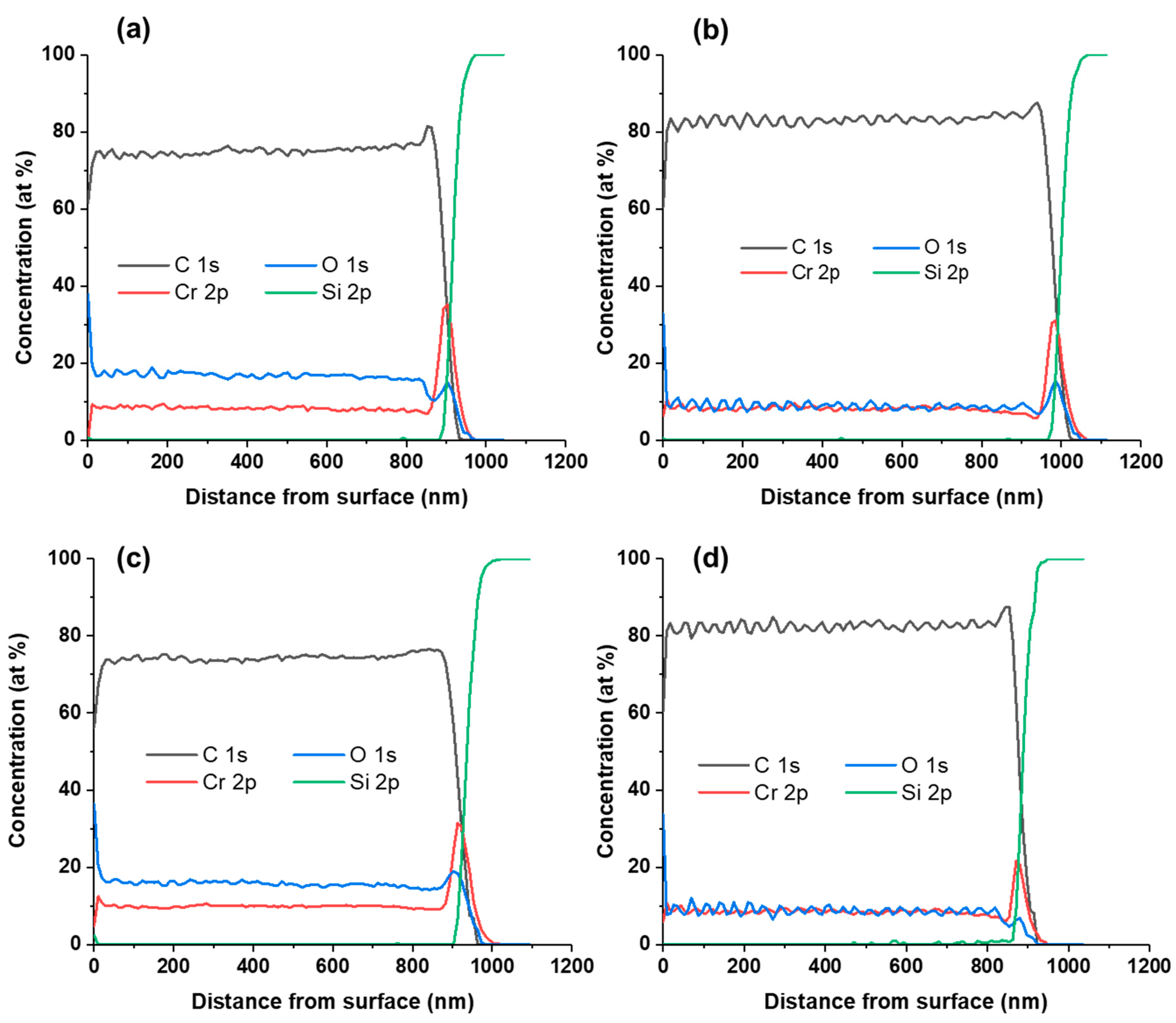
The chemical composition of the coatings as a function of depth has been obtained by XPS analysis and ERD analysis. A comparison of the chemical composition of the coatings as a function of the applied bias voltage and deposition pressure is illustrated in Figure 5. The C content slightly increases, whereas the oxygen (O) content decreases with increasing applied bias voltage at a constant amount of Cr for both groups. The presence of higher oxygen content through the coating is associated with the low deposition power and bombarding of the substrate with lower energy than usual in order to prevent overheating of the Kapton substrate as well as the recrystallization of the a-C:H:Cr coatings. Furthermore, even though the base pressure in an industrial system like the one employed for this work is 1 × 10 4 Pa, the oxygen concentration in the gas phase during deposition might be such that a small amount of oxygen is integrated into the films during the development due to the coater’s walls outgassing [31]. The decrease in O content with increasing bias voltage is known as a preferential sputtering effect, which removes adsorbed oxygen during coating growth. When the bias voltage increases, the sputtering and etching energy of ions or atoms increases, and atoms’ movement to the growing surface is enhanced. Due to the high deposition energy, C and Cr atoms are strongly bonded to the surface. Thus, weakly bonded O adatoms would be more easily re-sputtered by incident high-energy ions in the growth process of the coatings. This leads to dismissed O being replaced by C atoms [32] (extra information is listed in the Supplementary Materials).
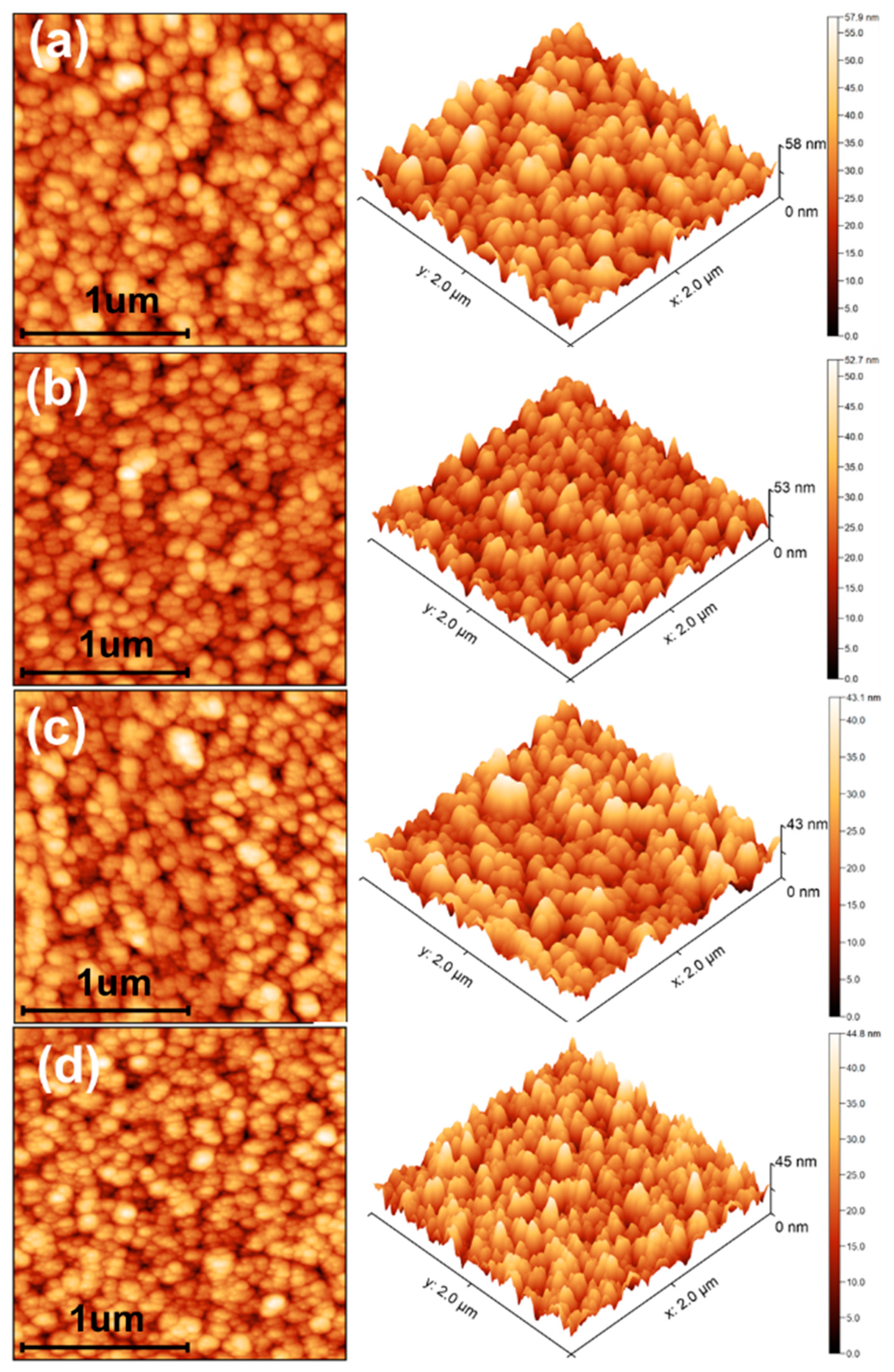
The AFM micrographs of the coatings over the 2 × 2 µm2 area of selected regions are given in Figure 6. The roughness significantly depends on the applied bias voltage and working pressure [33]. A clear distinction can be made based on the bias voltage: the coatings obtained without bias exhibit a larger root mean square (RMS) roughness besides exhibiting columns wider than the one produced with −100 V bias. Also, the working pressure seems to affect the roughness when no bias is applied: increasing the working pressure leads to a smoother surface. Hence, the application of bias during deposition has a prominent effect on surface morphology. Table 1 presents the column diameter and surface roughness measured by AFM.
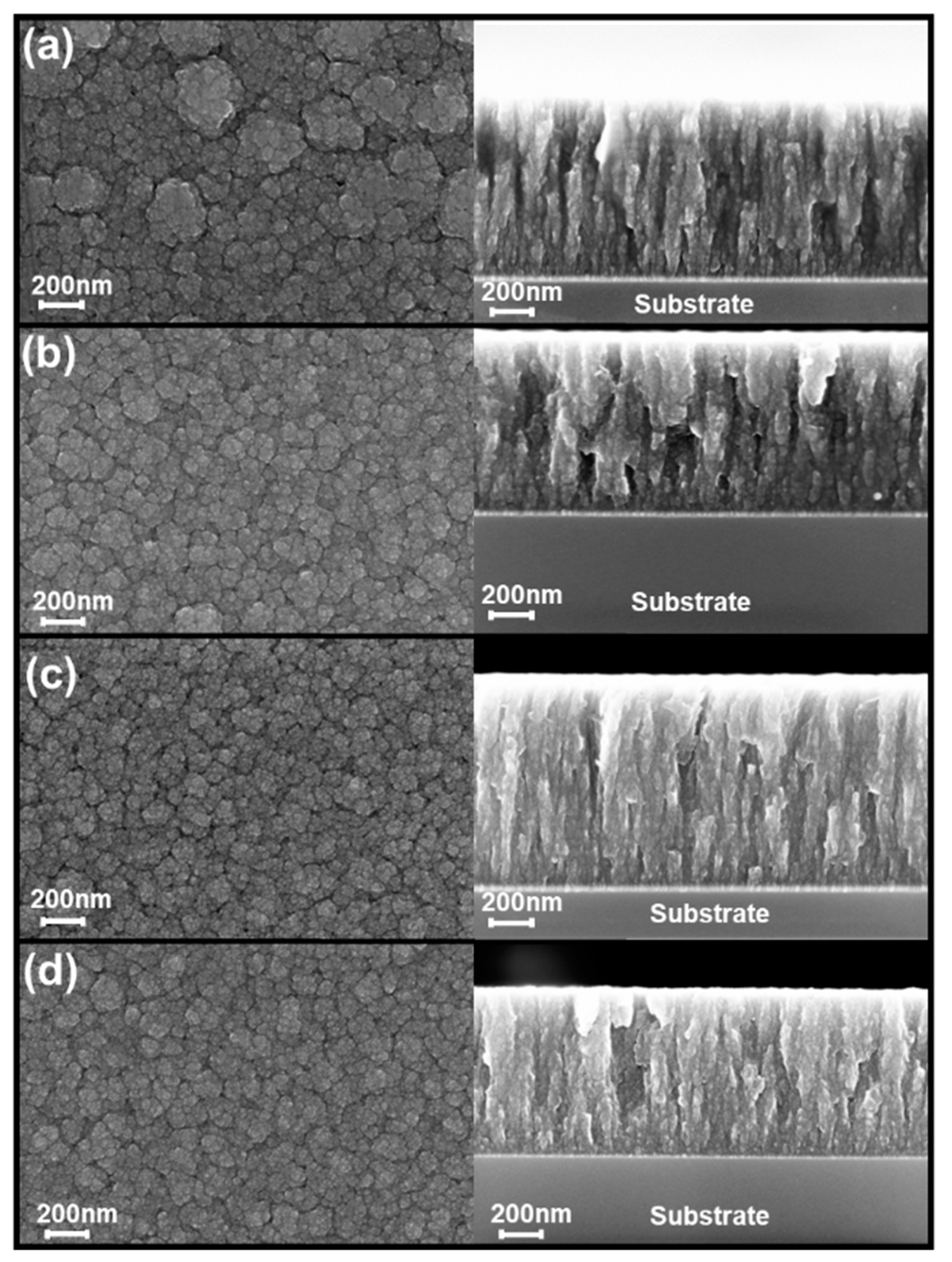
The SEM top view and cross-section micrographs (Figure 7) reveal additional microstructure characterization, which varies with pressure and bias voltage. Cross-sectional views indicate the presence of a morphological texture with a columnar ‘feature’ (by analogy to nanocrystalline thin coatings) parallel to the growth direction. AFM top view observation and SEM cross-sectional view are in qualitative agreement in the case of columnar growth of a-C:H:Cr coatings.

3.2. Mechanical and Tribological Properties

3.2.1. Nano-Indentation

The hardness (H) and Young’s modulus ( E ) are provided in Table 2. Coatings deposited without applied bias voltage are softer with a hardness of 3.52 ± 0.44 GPa and 3.06 ± 0.37 GPa for 0.66 Pa/floating and 2.66 Pa/floating, respectively. With an increasing bias voltage, the hardness gradually increases to reach the highest value (4.95 ± 0.69 GPa) for the 2.66 Pa/−100 V sample. Since during deposition, the temperature did not exceed the room temperature (30 °C), no relaxation takes place in the coatings [34]. For instance, residual compressive stress on the order of 700–800 MPa has been determined using the Stoney method for the 0.66 Pa/−100 V sample deposited on the Si wafer [35]. The compressive stress experienced in many a-C:H:Cr coatings tends to close the cracks during indentation preventing crack initiation and propagation while simultaneously showing the smallest indentation imprint. All coatings illustrate the same trend in Young’s modulus.
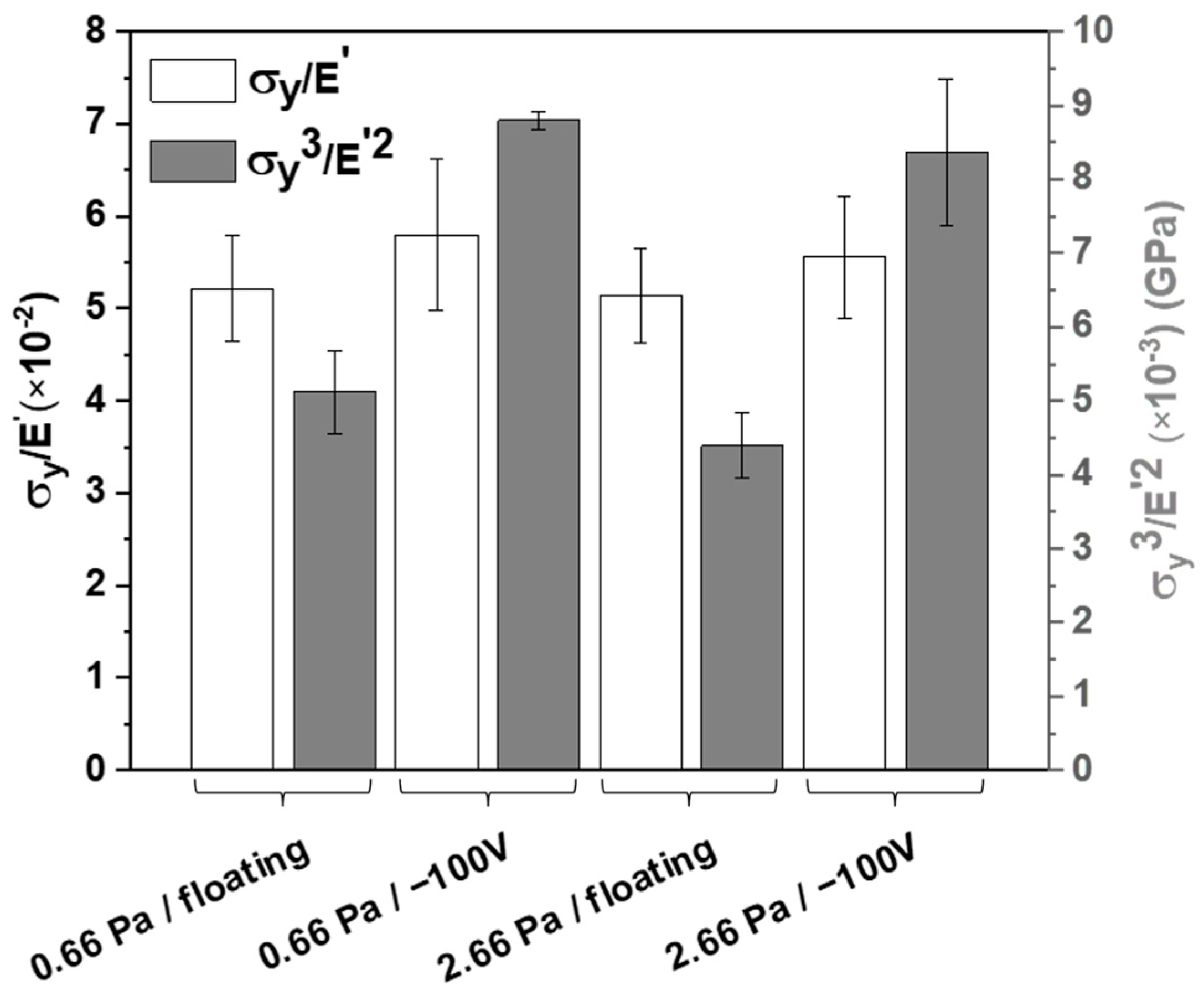
The performance indices σ y E and σ y 3 E 2   extracted from nanoindentation analysis are shown in Figure 8 and Table 2 as indicating the resistance of wear behavior and plastic deformation of coatings. The yield strength is estimated from the hardness (H) as
σ y = ξ 3 tan ( β ) H ξ 1 tan ( β ) ( 1 ξ 2 ) H E   ,
where ξ 1 ,   ξ 2 ,   ξ 3 , and β values for a Berkovich tip are equal to 0.66, 0.216, 0.24, and 19.7, respectively [36].
The apparent activation volume V * can be related to the physical activation volume Ω as V * = Ω γ where γ is the transformation strain associated with the local atomistic shuffling mechanism [37], which is the deformation mechanism expected for this class of amorphous solid. The value of γ for amorphous systems ranges from 0.05 to 0.15, see Argon [38]. We assume a transformation strain γ = 0.1 to obtain a rough estimate of the elementary volume in which the permanent elementary plastic deformation mechanism takes place. Figure 9 shows the variation of physical activation volume and the number of atomic sites involved in this volume as a function of the deposition parameters. The physical activation volumes obtained from relaxation tests also illustrate the same trend as for the nanoindentation results. Lower physical activation volume corresponds to coatings with larger hardness.
The lowest physical activation volume is found for the 2.66 Pa/−100 V thin coating as equal to Ω = 0.85 ± 0.11   nm 3 . When no bias is applied, the working pressure does not significantly affect the physical activation volume which is around 1.5 ± 0.23 nm3.

3.2.2. Wear Behavior

The wear behavior of the coatings has been directly evaluated by measuring the critical load at the onset of cracking ( L c ) as shown in Figure 10a. L c is defined as the load at which the coating fails under scratching conditions. Elastic recovery is also displayed as a function of sliding distance in Figure 10b. Total elastic recovery corresponds to 1 and fully plastic deformation corresponds to 0. 0.66 Pa/−100 V condition remains nearly fully elastic until it fails. The variation of L c for each material is displayed in Figure 10c. The bias voltage plays a major role in the enhancement of the coating resistance to wear. Also, the deposition working pressure seems to be significant, with the 0.66 Pa/−100 V sample being clearly more resistant to the onset of wear compared to the 2.66 Pa/−100 V one. The coefficient of friction is also an important index of the performance of an industrial coating (see Figure 10d). It must remain low even under high load.
The critical load for the onset of chipping increases by applying a bias voltage, see Figure 10 and Table 2. Whatever the working pressure, applying a bias voltage leads to an increase in the wear resistance of the a-C:H:Cr coatings. Figure 11 displays typical wear tracks produced by micro-scratching. Several features distinguish the materials failure modes: (i) the first chip forms at a critical load noted Lc propagates both forward and backward; (ii) the chip formation mechanism varies from random to reproducible chip sizes and shapes; (iii) a step-like pattern is evidenced along the crack surface. For 2.66 Pa coatings, the first chip propagates at a significantly lower critical load compared to 0.66 Pa coatings. This would imply that delamination at the interface between the Si wafer and a-C:H:Cr coating begins earlier—at a lower load—for the 2.66 Pa samples. The shape and the size of the chips depend on the bias voltage applied during deposition. Indeed, without bias, the chips are relatively diverse while for biased samples (−100 V), the chips are very reproducible. Also, for biased samples, chips are smaller and crack propagation is limited [10,39]. Finally, the fracture surface of the chip presents a step-like pattern as highlighted in Figure 11f. A qualitative counting of these features gives 20 occurrences. This is in line with the number of rotations performed during deposition (~23)—the samples being either close to the acetylene plasma or away. By getting far from the target, the risk of oxidation increases due to the absence of energetic ions bombarding the surface along the outermost surface of the coating, which produces a weaker interface for the next layers.

3.3. Uniaxial Tensile Tests

In-Situ SEM Tensile Tests

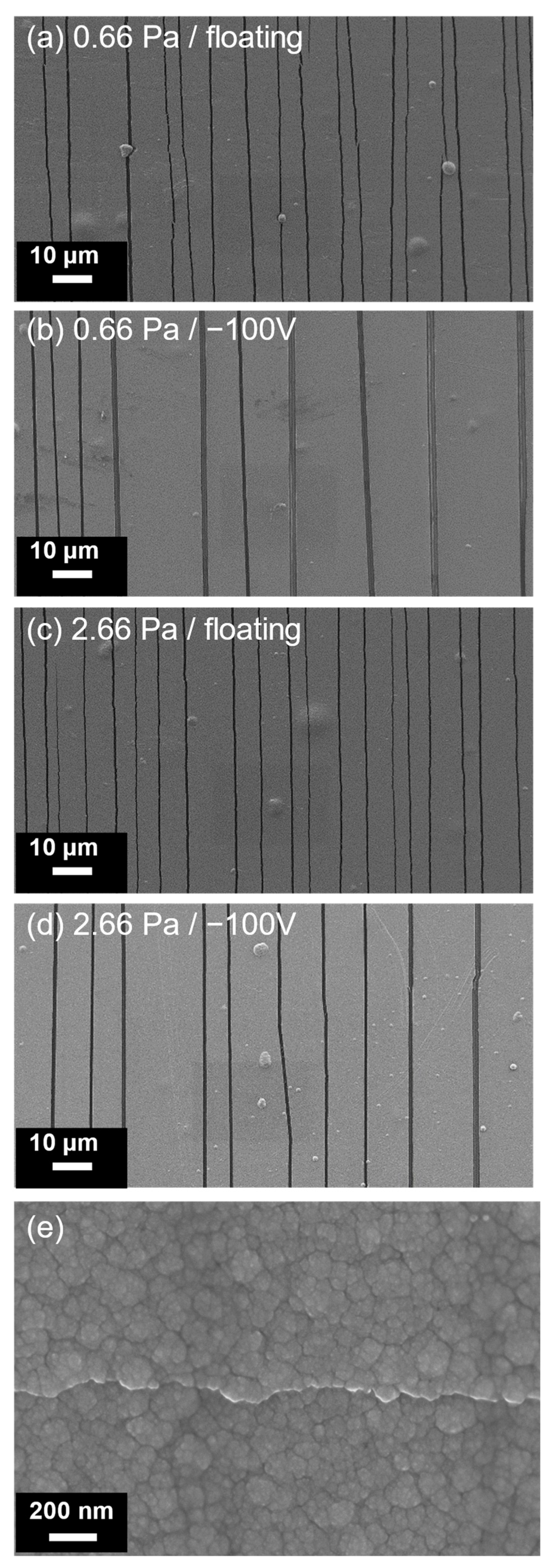
In order to determine the saturation crack density ( ρ s c ), 200× magnification SEM micrographs have been selected—i.e., with a typical 580 µm linear field of view to ensure statistically relevant measurements. Figure 12a–d shows crack patterns at 1 mm of crosshead displacement (at 1000× magnification in order to distinguish the cracks clearly) when saturation is reached. Increasing the bias voltage and decreasing the pressure leads to lower crack density and earlier saturation of the cracking process, see Table 3. Figure 12e shows a typical crack at very high magnification in a 2.66 Pa/−100 V thin coating. The cracks systematically propagate along the cluster boundary.
The fracture toughness of the coatings has been determined using Equation (4) with a Z factor equal to 15.6, as computed by [25] for a ratio H h   around 30 and a α-Dundurs parameter equal to 0.9. The plane strain Young’s modulus is obtained from nanoindentation experiments. The strain has been determined from in-situ optical microscopy tensile tests by taking the strain at which the first cracks start to propagate. K I c values of the different coating conditions are presented in Table 3 as well as the corresponding G I c . Increasing the working pressure leads to higher fracture toughness, as well as applying a bias voltage. Also, the application of a bias voltage decreases the crack density at saturation G I c values above 100 J/m2 which is an excellent resistance to cracking for a 1µm thick coating [40].

4. Discussion

4.1. Effect of Process Parameters on Hardness, Young’s Modulus, and Activation Volume

The magnitude of the hardness and Young’s modulus are in good agreement with similar a-C:H coatings from the literature. For instance, Wei et al. [41] measured hardness between 3–6 GPa, Kassavetis et al. [42] between 2–6 GPa, Vanden Brande et al. [43] around 4 GPa, and De vriendt et al. [44] around 7 GPa. Also, in these studies, Young’s modulus varies between 22.7–49.2 GPa, 20–45 GPa, 25–30 GPa, and 70 GPa, respectively.
By increasing the deposition pressure, ions are more likely to react with acetylene or to recombine with low-energy electrons. This leads to a reduction in the calculated ion mean free path from ≈22 mm to ≈5 mm and a rise in the number of collisions from 1.8 × 10⁴ collision/s at 0.66 Pa up to 7.2 × 10⁴ collision/s at 2.66 Pa. By knowing the target to substrate distance (≈150 mm) one can assume that number of collisions will increase from 1.2 × 10⁵ to 2.1 × 10⁶ collision/s from 0.66 Pa to 2.66 Pa, so it will decrease the energy of incident ions much more by increasing the deposition pressure. These reactions and recombination reduce the amount of energetic C2H2+ and Ar+ reaching the substrate. As a result of the sub-plantation process being reduced, energetic ion penetration into the growing coating will be prevented, which will lead to less sp3 bonding, which is a crucial characteristic of hard coatings [15,16,45,46]. Consequently, coating growth results from the condensation of low energetic species. In this case, growth will mostly be caused by the condensation of C2nH3 molecules which leads to a decrease in the hardness value [15,16]. Amorphous carbon coatings deposited from CaHb base without applied bias voltage are known to contain a higher density of C-H bonds which involve much smaller displacement energy than C-C bonds as present in a-C:H coatings [16], and coatings will contain a high amount of free volumes in their structure. When the bias voltage is applied, an increase in the energy of the ions impinging the substrate causes electron and carbon atoms to yield to compensate for free volume deficiency. This has been confirmed by the Raman spectroscopy results presented in Figure 4b and hardness values where the ID/IG decreases with increasing sp3 content at lower pressure and biased coatings. Although analyzing the ID/IG for a-C:H:Cr does not precisely reflect the hardness variation since the specimens are made up of two different elements rather than only carbon, the results may typically be used to identify patterns based on carbon structure. The increase in the coating hardness is associated with the decline in ID/IG [11].
There is also a relation between the applied bias voltage and the physical activation volume. Lower activation volumes are found when a bias voltage is applied during deposition, this would be another evidence of higher packing density [47]. Furthermore, assuming that the interatomic spacing of the surrounding C atoms is similar to the one of graphite, i.e., 0.34 nm [48,49] and that these sites present a spherical shape, we can estimate the volume of each site to be ≈0.16 nm3. These characteristics relate to crystalline C and do not represent the free volume of the amorphous structure of a-C:H:Cr. Nonetheless, the physical activation volume obtained from the nanoindentation test corresponds to 5 to 9 crystalline C atom sites. This suggests that the elementary volume where plastic deformation events occur is very localized and includes the motion of a few C atoms only. The lower the physical activation volume, the less the atoms will be involved in the viscoplastic deformation mechanisms which is favorable in terms of the mechanical stability of the coatings owing to higher strain rate sensitivity. Since the physical activation volume has the lowest value for biased samples, a stronger atomic arrangement of carbon clusters is expected as can also be seen from the elastic properties. The present results confirm that the effect of the bias voltage is predominant over the effect of deposition pressure.

4.2. Effect of Process Parameters on Wear Resistance

The critical load Lc at which scratch damages start appearing on the coating is used to qualify the wear resistance with a similar tip. In addition, the coating/substrate adhesion, the detachment of the fragments is also related to the cohesive (within the coating) fraction. The critical load has been shown to be proportional to the ratio σ y E quantifying the ability to deform elastically [50], which is in good agreement with what is observed here when applying a bias voltage (see Table 2). Again, applying a bias voltage results in enhanced scratch resistance. This is a known result, but this scenario is also in good agreement with the activation volume values. Note that even though the activation volume for 2.66 Pa/−100 V is lower than 0.66 Pa/−100 V, the critical load of the coating deposited under 0.66 Pa/−100 V is a bit higher. This can be explained by the weak interface adhesion between the Si substrate and the 2.66 Pa sample as compared to the adhesion of the 0.66 Pa coating. The key information extracted here is that a lower activation volume and higher σ y E and σ y 3 E 2   leads to a longer elastic track on the coating, delays the plastic deformation, and increases the critical load to the onset of crack.
Table 4 compares our results with other studies using the same deposition technique in the literature. Results are in good agreement with coatings made of comparable a-C:H:Me materials found in the literature. The choice of the target is important. Additionally, our results based on a metallic target and C2H2 precursor gas show a higher critical load than one obtained for coatings deposited from sputtering a graphite target.

4.3. Effect of Process Parameters on Fracture Behavior

The SEM micrograph of Figure 12e shows that the preferential crack path follows the boundary of columns. This highlights weaker inter-column boundaries. This is comparable to nano-glasses with weaker grain boundaries in comparison with the glassy matrix because of the higher free volume density contained in the boundaries [60]. However, the cluster interface strength also depends on the applied biased voltage. A decrease in columns’ size is found in samples with bias voltage, thus for the smaller clusters—i.e., a higher ratio of the interface to cluster—the crack resistance is the highest. If the interface strength is constant, a lower number of interfaces will lead to an enhanced crack resistance, whatever the applied bias. Indeed, increasing the bias voltage leads to an increase in the adatom energy. Thus, atoms will attach more firmly to the substrate and already present clusters. It is therefore confirmed that the cluster interface is stronger when a bias is applied, providing enhanced crack resistance [61].
Finally, the σ y E a performance indicator is plotted against the fracture energy ( G I c ) to compare the four different a-C:H:Cr coatings to an extensive list of thin coating materials gathered from the literature [62,63,64,65,66,67,68,69,70,71,72,73,74,75,76,77,78] in Figure 13. As an indicator of cracking resistance, the a-C:H:Cr coatings present the largest yield strength over Young’s modulus ratio with tunable G I c in the range of 5–125 J/m2.
Higher G I c and K I c values for 2.66 Pa samples can be directly related to their larger fracture strain and plastic process zone size which is more than two times larger than in 0.66 Pa coatings. Thus, by increasing the plastic process zone size, due to enhanced crack tip plasticity, the crack tip will be more blunted, and more energy will be needed to grow damage in the fracture process zone before material separation [79].
Accordingly, a-C:H:Cr coatings maintain a hardness that is substantially higher than that of elastomers while withstanding significant elastic deformation without showing signs of plasticity or failure. Also, the deposition conditions influence the coating toughness, and a relatively high critical energy release rate can be reached. This is of particular interest for applications where no residual scratches or imprints must remain after the contact. Protecting magnetic storage media from wear and corrosion due to their superior scratch resistance, bearings, gears, seals, engine components, oil media, and operation under ultra-high vacuum conditions are just a few of these applications [80,81,82]. Thus, according to the discussed properties, coatings with lower deposition pressure are attractive in applications where better adhesion and higher scratch resistance are needed. On the other hand, coatings with higher deposition pressure are beneficial for applications under extreme tension since they will exhibit larger fracture strain and fracture toughness.

5. Conclusions

The coating community often works to improve coating performances with different techniques using a trial-and-error approach. To the best of our knowledge, no rational material selection technique has been used yet to guide the optimization of a-C:H:Cr coatings based on targeted performance indices. In this work, we report a first effort in this direction to select the PECVD conditions in view of expected performances.
To this end, we evaluated the mechanical properties of four selected coatings deposited under different conditions (0.66 Pa, 2.66 Pa sputtering pressure, floating or −100 V bias voltage). Application of bias voltage was found dominant in terms of increasing the resistance to plastic deformation and wear resistance. Higher deposition pressure showed excellent resistance to cracking under tension, whatever the bias voltage.
A higher elastic limit (around 5%) was found when compared to a similar class of coatings in the industry while exhibiting tunable fracture toughness categorized in three different regimes of low (<10 J/m2), mid (10–100 J/m2), and high (>100 J/m2) levels.
Finally, this study proves that instead of focusing on specific parameters, it will be more beneficial to mix and match the mechanical properties in order to meet different lists of requirements associated with different types of applications.

Supplementary Materials

The following supporting information can be downloaded at: https://www.mdpi.com/article/10.3390/coatings13122084/s1, Figure S1. XPS depth profiling maps illustrate for a-C:H:Cr coatings show the presence of each element versus the etching time.

Author Contributions

Conceptualization, E.H., T.P. and S.L.; Methodology, A.B., P.B., M.-S.C. and H.I.; Formal analysis, A.B.; Data curation, A.B., P.B., M.-S.C., A.O. and H.I.; Writing—original draft, A.B.; Writing—review & editing, A.B., P.B., M.-S.C., A.O., H.I., E.H., T.P. and S.L.; Supervision, E.H., T.P. and S.L.; Project administration, T.P. and S.L.; Funding acquisition, T.P. and S.L. All authors have read and agreed to the published version of the manuscript.

Funding

This research was funded by the Walloon region under the PDR FNRS project number C 62/5—PDR/OL, semaphore 33677636. H. Idrissi acknowledge the financial support by the Belgian National Fund for Scientific Research (FSRFNRS) under Grant CDR—J.0113.20. M.-S. Colla acknowledges the financial support of National Fund for Scientific Reaserch (FNRS), Belgium.

Institutional Review Board Statement

Not applicable.

Informed Consent Statement

Not applicable.

Data Availability Statement

Data are contained within the article and Supplementary Materials.

Acknowledgments

The Synthesis, Irradiation & Analysis of Materials (SIAM), Morphology and Imaging (Morph-IM), and Physico-Chemical characterization (PC2) platform of Unamur, LACaMi and WELCOME platforms of UCLouvain, and EMAT platform of UAntwerpen are acknowledged for IBA, AFM & XPS, XRD, SEM, Raman spectroscopy and TEM facilities.

Conflicts of Interest

The authors declare that they have no known competing financial interest or personal relationships that could have appeared to influence the work reported in this paper.

References

  1. Tillmann, W.; Dias, N.F.L.; Stangier, D.; Schaak, C.; Höges, S. Heat treatment of binder jet printed 17–4 PH stainless steel for subsequent deposition of tribo-functional diamond-like carbon coatings. Mater. Des. 2022, 213, 110304. [Google Scholar] [CrossRef]
  2. Chodun, R.; Skowronski, L.; Trzcinski, M.; Nowakowska-Langier, K.; Kulikowski, K.; Naparty, M.; Radziszewski, M.; Zdunek, K. The Amorphous Carbon Thin Films Synthesized by Gas Injection Magnetron Sputtering Technique in Various Gas Atmospheres. Coatings 2023, 13, 827. [Google Scholar] [CrossRef]
  3. Neuville, S. New application perspective for tetrahedral amorphous carbon coatings. QScience Connect 2014, 2014, 8. [Google Scholar] [CrossRef]
  4. Fróis, A.; Aleixo, A.S.; Evaristo, M.; Santos, A.C.; Louro, C.S. Can a-C:H-Sputtered Coatings Be Extended to Orthodontics? Coatings 2021, 11, 832. [Google Scholar] [CrossRef]
  5. Sedlaček, M.; Podgornik, B.; Vižintin, J. Tribological properties of DLC coatings and comparison with test results: Development of a database. Mater. Charact. 2008, 59, 151–161. [Google Scholar] [CrossRef]
  6. Conde, F.F.; Diaz, J.A.Á.; Da Silva, G.F.; Tschiptschin, A.P. Dependence of wear and mechanical behavior of nitrocarburized/Crn/Dlc layer on film thickness. Mater. Res. 2019, 22. [Google Scholar] [CrossRef]
  7. Tamulevičius, S.; Meškinis, Š.; Tamulevičius, T.; Rubahn, H.-G. Diamond like carbon nanocomposites with embedded metallic nanoparticles. Rep. Prog. Phys. 2018, 81, 024501. [Google Scholar] [CrossRef]
  8. Popescu, A.C.; Stan, G.E.; Duta, L.; Nita, C.; Popescu, C.; Surdu, V.-A.; Husanu, M.-A.; Bita, B.; Ghisleni, R.; Himcinschi, C.; et al. The Role of Ambient Gas and Pressure on the Structuring of Hard Diamond-Like Carbon Films Synthesized by Pulsed Laser Deposition. Materials 2015, 8, 3284–3305. [Google Scholar] [CrossRef]
  9. Dai, W.; Gao, X.; Liu, J.; Wang, Q. Microstructure, mechanical property and thermal stability of diamond-like carbon coatings with Al, Cr and Si multi-doping. Diam. Relat. Mater. 2016, 70, 98–104. [Google Scholar] [CrossRef]
  10. Zawischa, M.; Weihnacht, V.; Kaspar, J.; Zimmermann, M. Effect of doping elements to hydrogen-free amorphous carbon coatings on structure and mechanical properties with special focus on crack resistance. Mater. Sci. Eng. A 2022, 857, 144086. [Google Scholar] [CrossRef]
  11. Zia, A.W.; Zhou, Z.; Li, L.K.-Y. Structural, mechanical, and tribological characteristics of diamond-like carbon coatings. In Nanomaterials-Based Coatings; Elsevier: Amsterdam, The Netherlands, 2019; pp. 171–194. [Google Scholar] [CrossRef]
  12. Li, G.; Xu, Y.; Xia, Y. Effect of Cr Atom Plasma Emission Intensity on the Characteristics of Cr-DLC Films Deposited by Pulsed-DC Magnetron Sputtering. Coatings 2020, 10, 608. [Google Scholar] [CrossRef]
  13. Weicheng, K.; Kangmei, L.; Jun, H.; Structure, T.E.; Property, N. and Adhesive Force of Magnetron-Sputtered Cr-DLC Coating on a Nitrided Ti6Al4V Alloy. J. Phys. Chem. C 2021, 125, 16733–16745. [Google Scholar] [CrossRef]
  14. Cui, X.-J.; Ning, C.-M.; Shang, L.-L.; Zhang, G.-A.; Liu, X.-Q. Structure and Anticorrosion, Friction, and Wear Characteristics of Pure Diamond-Like Carbon (DLC), Cr-DLC, and Cr-H-DLC Films on AZ91D Mg Alloy. J. Mater. Eng. Perform. 2019, 28, 1213–1225. [Google Scholar] [CrossRef]
  15. Fauroux, A.; Vandenabeele, C.; Pflug, A.; Lucas, S. Experimental and theoretical study of a magnetron DC-PECVD acetylene discharge: Determination of the main species and reactions taking place in the plasma. Surf. Coat. Technol. 2020, 400, 126195. [Google Scholar] [CrossRef]
  16. Fauroux, A.; Pflug, A.; Lucas, S. Experimental and theoretical study of a magnetron DC-PECVD acetylene discharge: Identification of the deposition precursors and film growth mechanisms. Surf. Coat. Technol. 2021, 421, 127472. [Google Scholar] [CrossRef]
  17. Greczynski, G.; Hultman, L. Compromising Science by Ignorant Instrument Calibration—Need to Revisit Half a Century of Published XPS Data. Angew. Chem. 2020, 132, 5034–5038. [Google Scholar] [CrossRef]
  18. Greczynski, G.; Hultman, L. X-ray photoelectron spectroscopy: Towards reliable binding energy referencing. Prog. Mater. Sci. 2020, 107, 100591. [Google Scholar] [CrossRef]
  19. Oliver, W.C.; Pharr, G.M. An improved technique for determining hardness and elastic modulus using load and displacement sensing indentation experiments. J. Mater. Res. 1992, 7, 1564–1583. [Google Scholar] [CrossRef]
  20. Hay, J.; Crawford, B. Measuring substrate-independent modulus of thin films. J. Mater. Res. 2011, 26, 727–738. [Google Scholar] [CrossRef]
  21. Gu, C.D.; Lian, J.S.; Jiang, Q.; Zheng, W.T. Experimental and modelling investigations on strain rate sensitivity of an electrodeposited 20 nm grain sized Ni. J. Phys. Appl. Phys. 2007, 40, 7440–7446. [Google Scholar] [CrossRef]
  22. Baral, P.; Orekhov, A.; Dohmen, R.; Coulombier, M.; Raskin, J.P.; Cordier, P.; Idrissi, H.; Pardoen, T. Rheology of amorphous olivine thin films characterized by nanoindentation. Acta Mater. 2021, 219, 117257. [Google Scholar] [CrossRef]
  23. Kim, K.; Luo, H.; Singh, A.K.; Zhu, T.; Graham, S.; Pierron, O.N. Environmentally Assisted Cracking in Silicon Nitride Barrier Films on Poly(ethylene terephthalate) Substrates. ACS Appl. Mater. Interfaces 2016, 8, 27169–27178. [Google Scholar] [CrossRef]
  24. Dundurs, J. Edge-bonded dissimilar orthogonal elastic wedges under normal and shear loading. J. Appl. Mech. Trans. ASME 1964, 36, 650–651. [Google Scholar] [CrossRef]
  25. Huang, R.; Prévost, J.H.; Huang, Z.Y.; Suo, Z. Channel-cracking of thin films with the extended finite element method. Eng. Fract. Mech. 2003, 70, 2513–2526. [Google Scholar] [CrossRef]
  26. Fu, K.; Chang, L.; Zheng, B.; Tang, Y.; Yin, Y. Analysis on cracking in hard thin films on a soft substrate under Berkovich indentation. Vacuum 2015, 112, 29–32. [Google Scholar] [CrossRef]
  27. Zhao, W.; Li, Y.; Wang, S.; He, X.; Shang, Y.; Peng, Q.; Wang, C.; Du, S.; Gui, X.; Yang, Y.; et al. Elastic improvement of carbon nanotube sponges by depositing amorphous carbon coating. Carbon 2014, 76, 19–26. [Google Scholar] [CrossRef]
  28. Ashby, M.F.; Greer, A.L. Metallic glasses as structural materials. Scr. Mater. 2006, 54, 321–326. [Google Scholar] [CrossRef]
  29. Wang, L.; Li, L.; Kuang, X. Effect of substrate bias on microstructure and mechanical properties of WC-DLC coatings deposited by HiPIMS. Surf. Coat. Technol. 2018, 352, 33–41. [Google Scholar] [CrossRef]
  30. Podgursky, V.; Alamgir, A.; Yashin, M.; Jõgiaas, T.; Viljus, M.; Raadik, T.; Danilson, M.; Sergejev, F.; Lümkemann, A.; Kluson, J.; et al. High-Temperature Tribological Performance of Al2O3/a-C:H:Si Coating in Ambient Air. Coatings 2021, 11, 495. [Google Scholar] [CrossRef]
  31. Bagherpour, A.; Haye, E.; Moskovkin, P.; Lucas, S. Vein pattern vs. columnar fracture shape in Cu-Zr thin film metallic glasses: Driving force and mechanism. Materialia 2023, 32, 101914. [Google Scholar] [CrossRef]
  32. Zhou, G.; Wang, L.; Wang, X.; Yu, Y.; Mutzke, A. Effect of bias voltage on microstructure and optical properties of Al2O3 thin films prepared by twin targets reactive high power impulse magnetron sputtering. Vacuum 2019, 166, 88–96. [Google Scholar] [CrossRef]
  33. Paul, A.; Lim, J.; Choi, K.; Lee, C. Effects of deposition parameters on the properties of chromium carbide coatings deposited onto steel by sputtering. Mater. Sci. Eng. A 2002, 332, 123–128. [Google Scholar] [CrossRef]
  34. Rohrbeck, M.; Körsten, S.; Fischer, C.B.; Wehner, S.; Kessler, B. Diamond-like carbon coating of a pure bioplastic foil. Thin Solid Films 2013, 545, 558–563. [Google Scholar] [CrossRef]
  35. Nix, W.D. Mechanical properties of thin films. Metall. Trans. A 1989, 20, 2217–2245. [Google Scholar] [CrossRef]
  36. Kermouche, G.; Loubet, J.L.; Bergheau, J.M. Extraction of stress–strain curves of elastic–viscoplastic solids using conical/pyramidal indentation testing with application to polymers. Mech. Mater. 2008, 40, 271–283. [Google Scholar] [CrossRef]
  37. van der Rest, A.; Idrissi, H.; Henry, F.; Favache, A.; Schryvers, D.; Proost, J.; Raskin, J.-P.; Van Overmeere, Q.; Pardoen, T. Mechanical behavior of ultrathin sputter deposited porous amorphous Al2O3 films. Acta Mater. 2017, 125, 27–37. [Google Scholar] [CrossRef]
  38. Argon, A.S. Inelastic behavior of non-polymeric glasses. Phys. Deform. Fract. Polym. 2013, 7, 174–227. [Google Scholar] [CrossRef]
  39. Geng, X.; Zhang, Z.; Barthel, E.; Dalmas, D. Mechanical behavior of stiff coating on glass under sliding contact. Wear 2010, 269, 351–361. [Google Scholar] [CrossRef]
  40. Freund, L.; Suresh, S. Thin Film Materials: Stress, Defect Formation and Surface Evolution. 2004. Available online: https://books.google.com/books?hl=en&lr=&id=9UNnzNYAkboC&oi=fnd&pg=PR16&dq=Freund+LB,+Suresh+S+(2003)+Thin+film+materials:+stress,+defect+formation,+and+surface+evolution.+Cambridge+University+Press,+Cambridge&ots=Ne0GJvVSvI&sig=j8MK9hv_e10_g9S6pWP0JchjwRc (accessed on 20 November 2023).
  41. Wei, X.; Chen, X.; Ren, X.; Lu, Q.; Zhang, L.; Wang, F. Polymeric amorphous carbon films with high hardness. Diam. Relat. Mater. 2017, 73, 253–259. [Google Scholar] [CrossRef]
  42. Kassavetis, S.N.; Logothetidis, S.; Matenoglou, G.M. Near-surface mechanical properties and surface morphology of hydrogenated amorphous carbon thin films. Surf. Coat. Technol. 2006, 200, 6400–6404. [Google Scholar] [CrossRef]
  43. Brande, P.V.; Lucas, S.; Winand, R.; Weymeersch, A.; Renard, L. Determination of the chemical and physical properties of hydrogenated carbon deposits produced by d.c. magnetron reactive sputtering. Surf. Coat. Technol. 1994, 68–69, 656–661. [Google Scholar] [CrossRef]
  44. De Vriendt, V.; Maseri, F.; Nonet, A.; Lucas, S. Study of Nanoparticles Formation in a Pulsed Magnetron Discharge in Acetylene. Plasma Process. Polym. 2009, 6, S6–S10. [Google Scholar] [CrossRef]
  45. Ji, M.; Jagodar, A.; Kovacevic, E.; Benyahia, L.; Poncin-Epaillard, F. Characterization of functionalized coatings prepared from pulsed plasma polymerization. Mater. Chem. Phys. 2021, 267, 124621. [Google Scholar] [CrossRef]
  46. Peng, J.; Liao, J.; Zhang, G.; Huang, J.; Qiu, X. Microstructure evolution and mechanical performance of tetrahedral amorphous carbon coatings with dense droplets during annealing. Mater. Chem. Phys. 2023, 301, 127697. [Google Scholar] [CrossRef]
  47. Wang, J.P.; Tan, L.P.; Liew, T.Y.F.; Low, T.S.; Wong, H.L.; Lee, Y.K. Effects of DC Bias on the Thermal Stability of DC In-Line Sputtered CoCrTa/Cr Thin Film Media. MRS Proc. 1998, 517, 273. [Google Scholar] [CrossRef]
  48. Harrison, W.A. Electronic Structure and the Properties of Solids: The Physics of the Chemical Bond; Courier Corporation: Washington, DC, USA, 2012. [Google Scholar]
  49. Bhushan, B. Chemical, mechanical and tribological characterization of ultra-thin and hard amorphous carbon coatings as thin as 3.5 nm: Recent developments. Diam. Relat. Mater. 1999, 8, 1985–2015. [Google Scholar] [CrossRef]
  50. Dai, W.; Shi, Y. Effect of Bias Voltage on Microstructure and Properties of Tantalum Nitride Coatings Deposited by RF Magnetron Sputtering. Coatings 2021, 11, 911. [Google Scholar] [CrossRef]
  51. Bruno, P.; Cicala, G.; Losacco, A.M.; Decuzzi, P. Mechanical properties of PECVD hydrogenated amorphous carbon coatings via nanoindentation and nanoscratching techniques. Surf. Coat. Technol. 2004, 180–181, 259–264. [Google Scholar] [CrossRef]
  52. Lu, X.; Li, M.; Tang, X.; Lee, J. Micromechanical properties of hydrogenated diamond-like carbon multilayers. Surf. Coat. Technol. 2006, 201, 1679–1684. [Google Scholar] [CrossRef]
  53. Constantinou, M.; Nikolaou, P.; Koutsokeras, L.; Avgeropoulos, A.; Moschovas, D.; Varotsis, C.; Patsalas, P.; Kelires, P.; Constantinides, G. Metal (Ag/Ti)-Containing Hydrogenated Amorphous Carbon Nanocomposite Films with Enhanced Nanoscratch Resistance: Hybrid PECVD/PVD System and Microstructural Characteristics. Nanomaterials 2018, 8, 209. [Google Scholar] [CrossRef]
  54. Nißen, S.; Heeg, J.; Wienecke, M.; Behrend, D.; Warkentin, M. Enhancing adhesion strength of a-C:H:Cu composite coatings on Ti6Al4V by graded copper deposition in a rf-PVD/PECVD hybrid process. Surf. Coat. Technol. 2018, 350, 659–671. [Google Scholar] [CrossRef]
  55. Beake, B.D.; Liskiewicz, T.W.; Vishnyakov, V.M.; Davies, M.I. Development of DLC coating architectures for demanding functional surface applications through nano- and micro-mechanical testing. Surf. Coat. Technol. 2015, 284, 334–343. [Google Scholar] [CrossRef]
  56. Lemoine, P.; Quinn, J.P.; Maguire, P.; McLaughlin, J.A. Comparing hardness and wear data for tetrahedral amorphous carbon and hydrogenated amorphous carbon thin films. Wear 2004, 257, 509–522. [Google Scholar] [CrossRef]
  57. Chen, Q.; Zeng, C.; Xu, M.; Yuan, H.; Lv, H.; Wang, Z.; Wang, X. Effect of SiNx interlayer thickness on adhesion and friction properties of diamond-like carbon films. Diam. Relat. Mater. 2019, 94, 186–193. [Google Scholar] [CrossRef]
  58. Beake, B.D.; Lau, S.P. Nanotribological and nanomechanical properties of 5–80 nm tetrahedral amorphous carbon films on silicon. Diam. Relat. Mater. 2005, 14, 1535–1542. [Google Scholar] [CrossRef]
  59. Beake, B.D.; Goodes, S.R.; Shi, B. Nanomechanical and nanotribological testing of ultra-thin carbon-based and MoST films for increased MEMS durability. J. Phys. Appl. Phys. 2009, 42, 065301. [Google Scholar] [CrossRef]
  60. Idrissi, H.; Ghidelli, M.; Béché, A.; Turner, S.; Gravier, S.; Blandin, J.-J.; Raskin, J.-P.; Schryvers, D.; Pardoen, T. Atomic-scale viscoplasticity mechanisms revealed in high ductility metallic glass films. Sci. Rep. 2019, 9, 13426. [Google Scholar] [CrossRef] [PubMed]
  61. Wang, Y.X.; Zhang, S.; Lee, J.W.; Lew, W.S.; Li, B. Influence of bias voltage on the hardness and toughness of CrAlN coatings via magnetron sputtering. Surf. Coat. Technol. 2012, 206, 5103–5107. [Google Scholar] [CrossRef]
  62. Ghidelli, M.; Gravier, S.; Blandin, J.J.; Djemia, P.; Mompiou, F.; Abadias, G.; Raskin, J.P.; Pardoen, T. Extrinsic mechanical size effects in thin ZrNi metallic glass films. Acta Mater. 2015, 90, 232–241. [Google Scholar] [CrossRef]
  63. Treml, R.; Kozic, D.; Schöngrundner, R.; Kolednik, O.; Gänser, H.-P.; Brunner, R.; Kiener, D. Miniaturized fracture experiments to determine the toughness of individual films in a multilayer system. Extrem. Mech. Lett. 2016, 8, 235–244. [Google Scholar] [CrossRef]
  64. Yang, L.W.; Mayer, C.R.; Chawla, N.; LLorca, J.; Molina-Aldareguía, J.M. Nanomechanical characterization of the fracture toughness of Al/SiC nanolaminates. Extrem. Mech. Lett. 2020, 40, 100945. [Google Scholar] [CrossRef]
  65. Triani, G.; Campbell, J.A.; Evans, P.J.; Davis, J.; Latella, B.A.; Burford, R.P. Low temperature atomic layer deposition of titania thin films. Thin Solid Films. 2010, 518, 3182–3189. [Google Scholar] [CrossRef]
  66. Hirakata, H.; Nishijima, O.; Fukuhara, N.; Kondo, T.; Yonezu, A.; Minoshima, K. Size effect on fracture toughness of freestanding copper nano-films. Mater. Sci. Eng. A 2011, 528, 8120–8127. [Google Scholar] [CrossRef]
  67. Jungk, J.M.; Boyce, B.L.; Buchheit, T.E.; Friedmann, T.A.; Yang, D.; Gerberich, W.W. Indentation fracture toughness and acoustic energy release in tetrahedral amorphous carbon diamond-like thin films. Acta Mater. 2006, 54, 4043–4052. [Google Scholar] [CrossRef]
  68. Merle, B.; Göken, M. Fracture toughness of silicon nitride thin films of different thicknesses as measured by bulge tests. Acta Mater. 2011, 59, 1772–1779. [Google Scholar] [CrossRef]
  69. Jonnalagadda, K.; Cho, S.W.; Chasiotis, I.; Friedmann, T.; Sullivan, J. Effect of intrinsic stress gradient on the effective mode-I fracture toughness of amorphous diamond-like carbon films for MEMS. J. Mech. Phys. Solids. 2008, 56, 388–401. [Google Scholar] [CrossRef]
  70. Hu, Y.; Huang, J.-H.; Zuo, J.-M. In situ characterization of fracture toughness and dynamics of nanocrystalline titanium nitride films. J. Mater. Res. 2016, 31, 370–379. [Google Scholar] [CrossRef]
  71. Chasiotis, I.; Cho, S.W.; Jonnalagadda, K. Fracture Toughness and Subcritical Crack Growth in Polycrystalline Silicon. J. Appl. Mech. 2005, 73, 714–722. [Google Scholar] [CrossRef]
  72. Hatty, V.; Kahn, H.; Heuer, A.H. Fracture Toughness, Fracture Strength, and Stress Corrosion Cracking of Silicon Dioxide Thin Film. J. Microelectromechanical Syst. 2008, 17, 943–947. [Google Scholar] [CrossRef]
  73. Han, S.Z.; Kang, J.; Kim, S.-D.; Choi, S.-Y.; Kim, H.G.; Lee, J.; Kim, K.; Lim, S.H.; Han, B. Reliable and cost effective design of intermetallic Ni2Si nanowires and direct characterization of its mechanical properties. Sci. Rep. 2015, 5, 15050. [Google Scholar] [CrossRef]
  74. Karimi, A.; Wang, Y.; Cselle, T.; Morstein, M. Fracture mechanisms in nanoscale layered hard thin films, Thin Solid Films. Thin Solid Films 2002, 420–421, 275–280. [Google Scholar] [CrossRef]
  75. Massl, S.; Thomma, W.; Keckes, J.; Pippan, R. Investigation of fracture properties of magnetron-sputtered TiN films by means of a FIB-based cantilever bending technique. Acta Mater. 2009, 57, 1768–1776. [Google Scholar] [CrossRef]
  76. Frank, S.; Handge, U.A.; Olliges, S.; Spolenak, R. The relationship between thin film fragmentation and buckle formation: Synchrotron-based in situ studies and two-dimensional stress analysis. Acta Mater. 2009, 57, 1442–1453. [Google Scholar] [CrossRef]
  77. Nasim, M.; Li, Y.; Wen, C. Length-scale dependent deformation, strengthening, and ductility of fcc/fcc Ni/Al nanolaminates using micropillar compression testing. Acta Mater. 2020, 193, 318–328. [Google Scholar] [CrossRef]
  78. Liu, Z.; Monclús, M.A.; Yang, L.W.; Castillo-Rodríguez, M.; Molina-Aldareguía, J.M.; LLorca, J. Tensile deformation and fracture mechanisms of Cu/Nb nanolaminates studied by in situ TEM mechanical tests. Extrem. Mech. Lett. 2018, 25, 60–65. [Google Scholar] [CrossRef]
  79. Preiß, E. Fracture Toughness of Freestanding Metallic Thin Films Studied by Bulge Testing: = Charakterisierung der Bruchzähigkeit freistehender metallischer Dünnschichten mittels Bulge-Experimenten; FAU University Press: Erlangen, Germany, 2018. [Google Scholar]
  80. Keunecke, M.; Bewilogua, K.; Becker, J.; Gies, A.; Grischke, M. CrC/a-C:H coatings for highly loaded, low friction applications under formulated oil lubrication. Surf. Coat. Technol. 2012, 207, 270–278. [Google Scholar] [CrossRef]
  81. Ronkainen, H.; Varjus, S.; Holmberg, K. Friction and wear properties in dry, water- and oil-lubricated DLC against alumina and DLC against steel contacts. Wear 1998, 222, 120–128. [Google Scholar] [CrossRef]
  82. Meunier, C.; Alers, P.; Marot, L.; Stauffer, J.; Randall, N.; Mikhailov, S. Friction properties of ta-C and a-C:H coatings under high vacuum. Surf. Coat. Technol. 2005, 200, 1976–1981. [Google Scholar] [CrossRef]
Figure 1. 1 m3 semi-industrial deposition chamber.
Coatings 13 02084 g001
Figure 2. Specimen geometry for tensile testing of a-C:H:Cr coatings on kapton.
Coatings 13 02084 g002
Figure 3. XRD pattern of the as-deposited amorphous coatings with different deposition conditions. The inset shows the high-resolution TEM micrograph and a diffraction pattern typical of amorphous coating.
Coatings 13 02084 g003
Figure 4. (a) Raman spectra of the a-C:H:Cr coatings. (b) Variation of the ID/IG intensity ratio and the G peak positions under different deposition conditions.
Coatings 13 02084 g004
Figure 5. Chemical composition obtained by XPS depth profiling as a function of the coating thickness for (a) 0.66 Pa/floating and (b) 0.66 Pa/−100 V, (c) 2.66 Pa/floating, and (d) 2.66 Pa/−100 V conditions.
Coatings 13 02084 g005
Figure 6. AFM images of a-C:H:Cr coatings (a) 0.66 Pa/floating and (b) 0.66 Pa/−100 V, (c) 2.66 Pa/floating, and (d) 2.66 Pa/−100 V.
Coatings 13 02084 g006
Figure 7. SEM micrographs on top views and cross-sections of a-C:H:Cr coatings: (a) 0.66 Pa/floating and (b) 0.66 Pa/−100 V, (c) 2.66 Pa/floating, and (d) 2.66 Pa/−100 V.
Coatings 13 02084 g007
Figure 8. Comparison of the performance indices:   σ y E and σ y 3 E 2 for the four conditions investigated in this study. The error bars represent the standard deviation calculated over 16 experiments.
Coatings 13 02084 g008
Figure 9. Effect of the deposition parameters on the physical activation volume and associated number of atomic sites of a-C:H:Cr thin coating. Arrows are for the identification of y-axes.
Coatings 13 02084 g009
Figure 10. Results from the nanoscratch tests: (a) typical scratch profile with the displacement during loading as a black plain line and the profile of the wear track after loading in a dashed black line. The black arrow indicates the location of the critical load; (b) variation of the elastic recovery as a function of the sliding distance; (c) average critical load measured for each coating, error bars indicate the standard deviation; (d) variation of the coefficient of friction as a function of the sliding distance.
Coatings 13 02084 g010
Figure 11. Typical wear track after nano-scratch testing of (a) 0.66 Pa/floating and (b) 0.66 Pa/−100 V, (c) 2.66 Pa/floating, and (d) 2.66 Pa/−100 V. The white arrows indicate the location of the critical load. The blue box highlights in (e) the formation of a chip just after the critical load on a 0.66 Pa/−100 V sample. The red box displays in (f) the crack features of the chip. The dashed white lines highlight the step-like pattern produced during the formation of the chip.
Coatings 13 02084 g011
Figure 12. (ad) Evolution of crack density with in-situ strain for different samples (e) typical high magnification SEM top-view observation of a crack.
Coatings 13 02084 g012
Figure 13. Materials property map presenting the ratio yield strength over Young’s modulus against critical energy release rate. The results are obtained from the literature and compared to the four a-C:H:Cr thin coatings produced in this study [62,63,64,65,66,67,68,69,70,71,72,73,74,75,76,77,78].
Coatings 13 02084 g013
Table 1. a-C:H:Cr coatings mean column diameter and surface RMS roughness measured by AFM.
SampleColumn Diameter (nm)Surface RMS Roughness (nm)
0.66 Pa/floating31.5 ± 2.67.8 ± 0.16
0.66 Pa/−100 V24.7 ± 0.76.2 ± 0.01
2.66 Pa/floating31.7 ± 1.66.7 ± 0.81
2.66 Pa/−100 V29.1 ± 1.66.2 ± 0.14
Table 2. Nano-indentation and micro-scratch related results: hardness, Young’s modulus, resistance to plastic deformation, wear resistance, and critical load values for different deposition conditions.
H
(GPa)
E
(GPa)
σ y E × 10 2 σ y E 2 3 × 10 3
(GPa)
L c
(mN)
0.66. Pa/floating3.5 ± 0.436.2 ± 2.85.21 ± 0.575.12 ± 0.5650 ± 1.3
0.66 Pa/−100 V4.7 ± 0.845.1 ± 4.35.80 ± 0.818.80 ± 0.1263.7 ± 2.0
2.66 Pa/floating3.1 ± 0.432.3 ± 1.95.15 ± 0.514.40 ± 0.4348.4 ± 10.7
2.66 Pa/−100 V4.9 ± 0.748.7 ± 3.95.60 ± 0.658.37 ± 0.9957.7 ± 1.2
Table 3. Traction related results: Saturation crack density at 1 mm of crosshead displacement, critical fracture energy release rate, fracture toughness, and fracture plastic zone size values for different deposition conditions.
ρ s c
(µm−1)
G I c
(J/m2)
K I c
(MPa·m1/2)
d
(nm)
0.66 Pa/floating0.128 ± 0.0044.94 ± 0.040.42 ± 0.0815.7 ± 0.82
0.66 Pa/−100 V0.049 ± 0.00147.4 ± 0.831.46 ± 0.05100.8 ± 1.08
2.66 Pa/floating0.173 ± 0.002125 ± 5.632.01 ± 0.18488.6 ± 2.68
2.66 Pa/−100 V0.1 ± 0.003115 ± 2.952.37 ± 0.12242.5 ± 1.55
Table 4. a-C:H:Cr coatings deposited by PECVD method with CH4 and C2H2 precursor gases or graphite target and nano-indentation results in comparison with recent work.
SamplePrecursor Gas/Source H E Lc (mN)
Ref. [51]CH40.124–0.13433–64
Ref. [52]CH40.11–0.1643–120
Ref. [53]CH4-18.2–23.5
Ref. [54]C2H20.041–0.08636–75
Ref. [55]C2H20.08168
Ref. [56]C2H20.0672.13
Ref. [57]Graphite0.146
Ref. [58]Graphite≈0.0831.9–5
Ref. [59]Graphite≈0.08140
Our studyC2H20.09–0.148–64
Disclaimer/Publisher’s Note: The statements, opinions and data contained in all publications are solely those of the individual author(s) and contributor(s) and not of MDPI and/or the editor(s). MDPI and/or the editor(s) disclaim responsibility for any injury to people or property resulting from any ideas, methods, instructions or products referred to in the content.