Article

Characterization and Growth of TiO2/ZnO on PTFE Substrates at Different Volumetric Ratios Using Chemical Bath Deposition

by
Youssif S M Elzawiei
,
Md Roslan Hashim
*,
Mohd Mahadi Halim
and
Abdullah Abdulhameed
Nano-Optoelectronics Research and Technology Laboratory (NOR), School of Physics, Universiti Sains Malaysia, Penang 11800 USM, Malaysia
*
Author to whom correspondence should be addressed.
Coatings 2023, 13(2), 379; https://doi.org/10.3390/coatings13020379
Submission received: 31 December 2022 / Revised: 28 January 2023 / Accepted: 31 January 2023 / Published: 7 February 2023

Abstract

:
Developing non-toxic, semiconductor-doped heterojunction materials for optoelectronic applications on the surface of a flexible substrate is a viable strategy for meeting the world’s energy needs without introducing any environmental issues. In this paper, Ti:TiO2/ZnO nanocomposites were prepared by heat treatment and utilized as an active layer in UV photodetectors. First, a ZnO seed layer was deposited by radio frequency (RF) sputtering on polytetrafluoroethylene (PTFE) substrates. Then, TiO2/ZnO thin films (TFs) were successfully grown by combining volumetric mixtures of TiO2 and ZnO at the ratios of 1:7, 1:3, 3:5, and 1:1 via the chemical bath deposition (CBD) method. The morphological, elemental, and topographical analyses of the grown TFs were investigated through SESEM, EDX, and AFM spectroscopy, respectively. XRD patterns illustrated the presence of the unified (002) peak of the Ti/ZnO hexagonal wurtzite structure in all prepared samples, with intensities indicating a very strong preferential crystallinity with increasing TiO2 ratios. Enhanced diffuse reflectance curves were obtained by UV–Vis spectroscopy, with allowed indirect energy bandgaps ranging from 3.17 eV to 3.23 eV. FTIR characterization revealed wider phonon vibration ranges indicating the presence of Ti–O and Zn–O bonds. Metal–semiconductor–metal (MSM) UV photodetectors were fabricated by thermally evaporating Ag electrodes on the grown nanocomposites. The volumetric ratio of TiO2/ZnO impacted the photodetector performance, where the responsivity, photosensitivity, gain, detectivity, rise time, and decay time of 0.495 AW−1, 247.14%, 3.47, 3.68 × 10⁸ jones, 0.63 s, and 0.99 s, respectively, were recorded at a ratio of 1:1 (TiO2:ZnO). Based on the results, the heterostructure nanocomposites grown on PTFE substrates are believed to be highly promising TF for flexible electronics.

1. Introduction

The outstanding characteristics associated with zinc oxide (ZnO), including wide energy gap (Eg) and high electronic mobility, attract interest in nanophotonic applications [1]. Despite the concern of fast electron–hole (e-h+) recombination of this metal oxide, the interstitial levels between the valence band (VB) and conduction band (CB) have aided in deterring the occurrences of fast recombination of photogenerated charge carriers [2]. Of the many metal oxides, titanium dioxide (TiO2) is one of the most widely studied semiconductor materials for nanophotonic applications [3,4]. ZnO and TiO2 are known to have some properties in common, such as wide energy band gaps, non-toxic compounds, chemical stability, and being inexpensive [5,6,7].
Several research centers and groups have ongoing research for decades in synthesizing nanomaterials that can absorb photons, leading to the excitation of electrons for diverse applications [8,9]. Further, the construction of heterojunctions between composite semiconductors with staggered band alignment has become common and considerable in controlling the photoinduced charge migration across the interface, where the electric potential provides the driving force for the controllable charge migration [2,5].
The methods used in the synthesis of nanomaterials have often depended on the nature of the nanomaterials involved, device scale, compatibility, and cost [10]. The chemical bath deposition (CBD) method is one of the standard methods to synthesize nanomaterials due to its numerous advantages, such as being inexpensive, requiring less complex machinery or procedures, having an easily controlled growing time, a low operating temperature, and the ability to create optimized nanocomposites with various morphologies and properties on large areas of different substrates [11,12,13].
In addition, the CBD technique has often been conducted in open systems, where nano-sedimentation occurs in an open beaker [14]. The open-beaker system technique is typically a long-duration process in which the system is subjected to temperature changes over long periods of time, which may cause the nanostructure to change and result in a poorly adapted processing framework that is not well suited to the subjected synthesis process [15,16,17]. Recently, the low-cost, less energy-consuming (thermodynamically closed system) Duran laboratory bottle has been utilized as an alternative to the open beaker for CBD processes [18]. Moreover, several materials have been used as substrates in the CBD process, such as glass, p-type silicon, and n-type silicon [19,20,21,22]. However, using polytetrafluoroethylene (PTFE), or so-called Teflon, as a substrate in a closed growth system is rarely reported. This versatile, flexible, high-performance commodity polymer is also easily producible, recyclable, and substantially less expensive [23].
Although CBD has still been widely used in the synthesis and growth of different ZnO nanostructures, there is a decrease in the reports that optimize the growth of doped ZnO [21,24], particularly with Ti as Ti/ZnO and TiO2 as TiO2/ZnO. Further, the reports regarding the growth of Ti/ZnO and TiO2/ZnO nanostructures on PTFE substrate via the CBD method are extremely rare [25,26,27], while the impact of the TiO2/ZnO volumetric ratio—grown using this method on the mentioned substrate—on the performance of photodetector devices has never been reported [28,29].
Metal–semiconductor–metal (MSM) photodetectors have garnered considerable interest in the optoelectronics field due to their ease of design, fast response, large active area, and variation in the values of the photoinduced electric current [30,31,32]. Nonetheless, despite the fact that the various literature has established Ti is a significant dopant for the enhancement of both electrical and optical properties, the literature survey contains few reports that investigate the influence of doping ZnO with Ti and TiO2 to enhance the characteristics and performance of UV photodetectors.
This work reports an improved photocatalytic ZnO via synthesized Ti:TiO2/ZnO on PTFE substrates using the CBD method. The method combines the integration of TiO2 to form a composite material while paying attention to volumetric control of the ratios of the participating precursors during the CBD synthesis. The physical, structural, and optical characteristics of synthesized nanocomposites were studied using field emission scanning electron microscope (FESEM), Atomic Force Microscopy (AFM), X-ray diffraction (XRD), Ultraviolet–visible–near infrared (UV–Vis–NIR), and Fourier-transform infrared (FTIR) spectroscopies. Furthermore, UV photodetectors were fabricated, and their photoresponse and I–V curves were investigated. Apart from making a composite structure with TiO2, the introduction of Ti metal as a dopant to form Ti:TiO2/ZnO is believed to be a promising way of improving the photocatalytic performance of ZnO. The improvements in ZnO through doping with Ti:TiO2 enable UV photodetectors to be implemented in several applications, including communications, ozone sensing, air purification, flame sensing, and leak detection [33].

2. Experimental Methods

2.1. Materials and Chemicals

Zinc nitrate hexahydrate (Zn(NO3)6·H2O, Sigma-Aldrich Assay (Sigma-Aldrich, St. Louis, MO, USA) ≥ 99% purity), hexamethylenetetramine (C6H12N4, Sigma-Aldrich, Assay ≥ 99% purity), TiO2 powder (TiO2, Fluka Chemika (St. Louis, MO, USA), Assay > 99% purity), ethanol (99.9% purity), laboratory Duran bottles (Duran, Duisburg, Germany), Polytetrafluoroethylene (PTFE) sheets with a thickness of 1.5 mm, isopropyl alcohol (C3H8O, 99.7% purity), ZnO target with a diameter of 60 mm (99.999% purity), deionized water (DI), interdigitated electrode (IDE) shadow mask, and silver wire for thermal evaporation (Ag 99.99% purity).

2.2. Synthesis of (Ti:TiO2/ZnO)@ZnO TFs

Zinc nitrate hexahydrate and hexamethylenetetramine were prepared at a concentration of 0.05 M and then combined at a ratio of 1:1 to form ZnO precursors. Each of the precursors was dissolved separately using a magnetic stirrer at 60 °C for 15 min before mixing them in a Duran bottle under similar conditions to ensure a homogeneous mixture. TiO2 nanofluid was prepared by adding 1 g of TiO2 powder to 70 mL of ethanol inside a different Duran bottle. The nanofluid was processed under a sonication system (Branson heated Ultrasonic cleaner-2510 MTH-40 kHz (Branson, Branson, MO, USA)) at 60 °C for 5 h to mix the nonhomogeneous liquid vigorously [34].
PTFE substrates were prepared in a dimension of 1 cm2 and were cleaned by ultrasonication in isopropyl alcohol at 60 °C for 20 min and washed with deionized (DI) water for 1 min each. A 100 nm seed layer was sputtered from a ZnO target material to form a thin film (TF) coating the PTFE substrates. The RF sputtering was conducted at a working pressure of 5 × 10⁻⁵ mbar and power of 150 W in argon gas with a flow rate of 9.99 sccm (HHV-AUTO 500). The samples were then annealed in a conventional furnace (Lenton Thermal Designs (Lenton, Palmdale, CA, USA)) at 150 °C for 30 min in a normal room environment.
For CBD, the Duran bottles were cleaned carefully, and the samples were put in a vertical position before different amounts of the precursor solution and nanofluid were added. The percentages of TiO2:ZnO were 1:7, 1:3, 3:5, and 1:1 (40 mL:40 mL). These ratios were chosen based on the volume of the Duran laboratory bottle, which has a total volume of 80 mL. The bottles containing the substrates with mixtures (ZnO precursor and TiO2 nanofluid) at different ratios were then placed into an oven for 5 h at a temperature of 96 °C Later, the samples were rinsed in DI water and then dried in air. The synthesized samples were labeled according to the above ratios as S1, S2, S3, and S4, respectively. Finally, the samples were kept at 16 °C for 24 h prior to proceeding with the characterizations under normal ambient conditions.

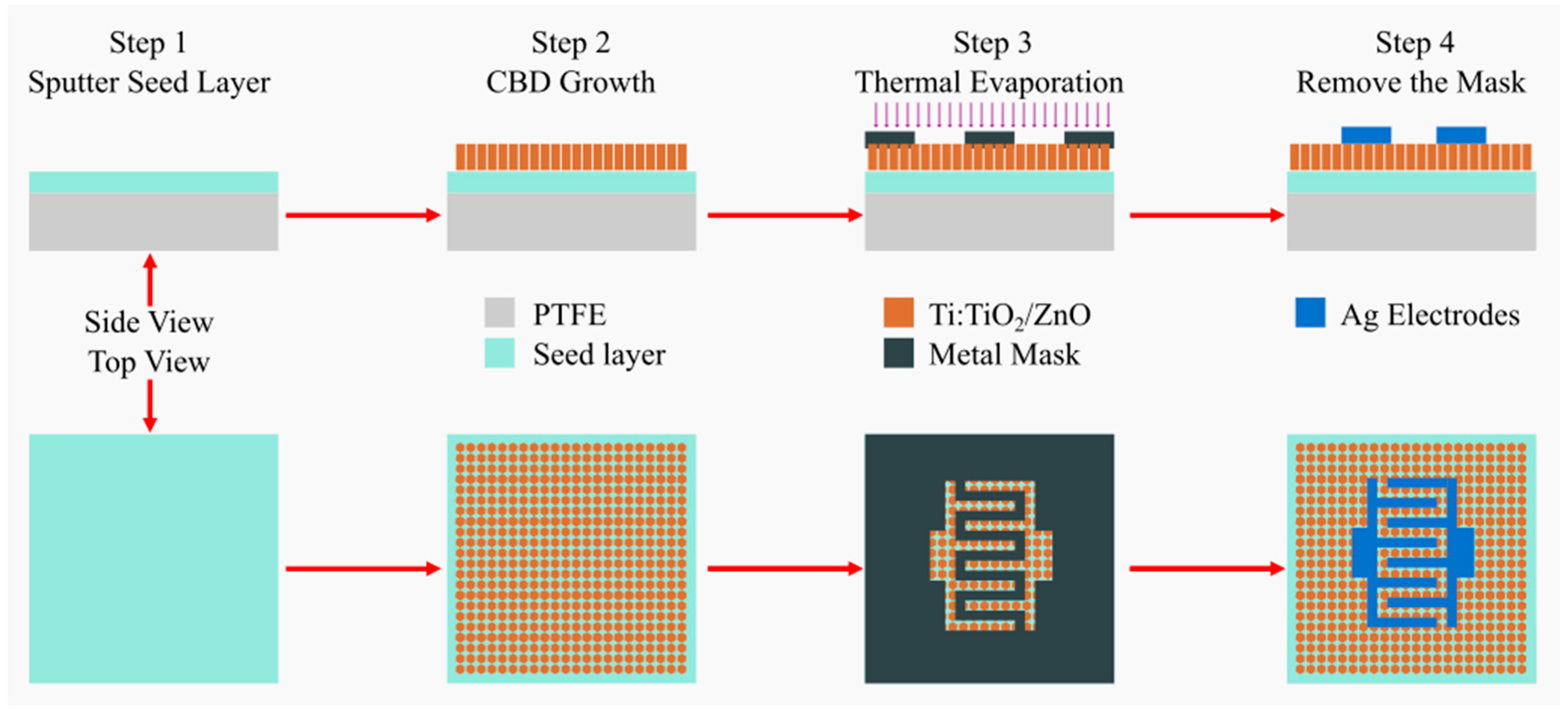
2.3. Fabrication of MSM Photodetectors

The fabrication of the MSM photodetectors can be summarized in four steps, as illustrated in Figure 1. The first and second steps were explained in the previous section, which includes ZnO TF seed layer sputtering and the CBD growth of the Ti:TiO2/ZnO layer. In the third step, a metal mask with interdigitated electrode (IDE) design was placed on the synthesized semiconductor layer. Vacuum thermal evaporation was used to deposit silver (Ag) electrodes on the top of the sample. The metal mask was then removed, leaving a printed IDE structure on the sample surface, as shown in the fourth step in Figure 1. The IDE consists of two electrodes with four fingers each that make up the MSM (Ag/Ti:TiO2/ZnO/Ag) photodetector; the distance between each finger is 0.4 mm, and each finger is 0.35 mm wide and 3.4 mm long. The procedure was applied for samples S1, S2, S3, and S4, representing photodetectors with TiO2:ZnO ratios of 1:7, 1:3, 3:5, and 1:1, respectively.

2.4. Characterization

Surface morphology characterization and composition analysis of the synthesized material was carried out on the prepared films using FESEM and EDX (FEI Nova NanoSEM 450, Hillsboro, Oregon, USA). Atomic Force Microscopy (AFM) (Model: Dimension EDGE, BRUKER, Hamburg, Germany) was used to study the surface roughness as well as the peak, valley, and topographical analysis. The phase and crystallinity of the films were examined using a high-resolution XRD instrument (PANalytical X’pert PRO, Netherlands) with CuKα (λ = 0.15406 nm) radiation source. Optical diffused and reflectance measurements were employed using Cary 5000 Agilent Tech UV–Vis–NIR spectrophotometer (Cary, Addison, IL, USA). Fourier-transform infrared (FTIR) spectroscopy (Perkin Elmer Spectrum GX FTIR, Buckinghamshire, UK) was utilized to determine the bonds between the molecules and the phonon properties. The photoresponse properties were obtained by exposing the samples to a UV source (2.83 mW/cm2, and 365 nm) and measuring the current–voltage (I–V) response using a semiconductor characterization system (Keithley-2400SCS (Keithley, Cleveland, OH, USA)) connected to PC for data analysis.

3. Results and Discussion

3.1. Formation Mechanisms of ZnO and Ti:TiO2/ZnO

The formation of the final composites can be explained in three stages: disassembling TiO2 through sonication, growth of ZnO, and dopant attachment. In the first stage, TiO2 nanoparticles (NPs) in the form of TiO2 nanofluid were created by sonicating a mixture of TiO2 powder and ethanol at a low temperature for five hours before conducting the CBD. The organic solution was used to disassemble TiO2 molecules by unbinding TiO2, yielding Ti ions accompanied by TiO2 residual NPs, and increasing the negativity of hydrocarbonate and hydroxyl groups, as shown in Equations (1) and (2). There is a possibility that T i 4 + ions resulted from Ti atoms along the process (Equation (3)), in which case the ions combined with H2O that had separated from the organic solvent and rebuilt TiO2 again in the form of NPs, as can be seen in Equation (4). Another possibility is that Ti atoms, which had been released from their bonds by sonication, joined with H2O molecules that were broken up from the organic solvent and resulted in TiO2 and negative charges, as described in Equation (5) [35,36]. The reaction balance of chemical equations is labeled with m, m*, n, n*, k, h, and j.
m ( TiO 2 ) + n ( C H O )   sonication ( TiO 2   NPs ) m .   ( C 2 H 6 O ) n
( TiO 2   NPs )   m .   ( C 2 H 6 O )   n   sonication   k ( Ti   ions )   +   h   ( TiO 2   residual   NPs )   +   j   ( negativity   hydrocarbonte   + hydroxil   groups )
Ti   sonication   Ti 4 + + 4 e
Ti 4 + + 2 H 2 O sonication   TiO 2 + 4 H +
Ti + 2 H 2 O sonication   TiO 2 + 4 H + + 4 e
In the second stage, the ZnO nanorods grew from their precursor at a specific temperature through nucleation. First, OH is produced from the hexamethylenetetramine, as described by Equations (6) and (7). Once the concentrations of Zn2+ (resulting from zinc nitrate hexahydrate) and OH reached saturation at the temperature of 96 °C, rapid nucleation of ZnO occurred, as described by Equations (8) and (9) [25].
C6H12N4 + 6H2O → 6HCHO + 4NH3
NH 3 + H 2 O     NH 4 + + OH
Zn 2 + + 2 OH     ZnO + H 2 O   ( nuclei )   +   H 2 O
Zn OH 4 2     ZnO + H 2 O + 2 OH
In the third stage, which occurs simultaneously as the ZnO NRs grow, Ti and TiO2 incorporate with ZnO in different mechanisms. Since the radius of the Ti4+ ion is less than the radius of the Zn2+ ion, there is a possibility that they joined each other while the other Ti ions were diffused in the ZnO, and thus Ti-doped ZnO (Ti:ZnO) was produced [37]. It is also possible that Ti might dope the nanocomposites through Ti ions self-doping TiO2 (Ti:TiO2) and Ti-doped TiO2/ZnO (Ti:TiO2/ZnO). The presence of Ti4+ has a significant effect on the activation in the photocatalytic process because it inhibits oxidation [38,39].

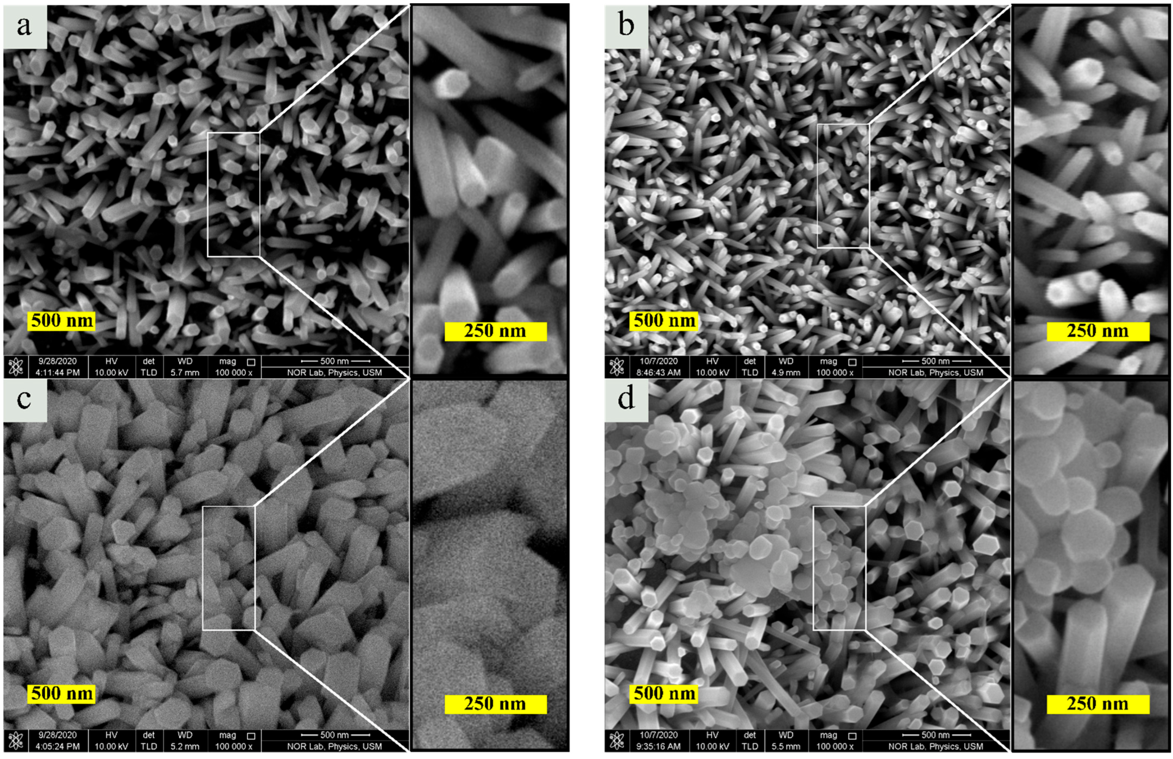
3.2. Morphology and Elemental Composition

Figure 2 shows the morphologies of the homoepitaxial and heteroepitaxial layers grown with the incorporation of nanocomposites on PTFE substrates at different volumetric ratios of TiO2 to ZnO. The images reveal that the growth of the nanocomposite samples has aligned and semi-aligned mixed nanorod (NR) arrays on the substrates due to the high thermal coefficient of the PTFE substrate [40,41]. It is evident that the increase in the density and size of the NRs appears as a result of the incorporation of Ti ions (cation) into the interstitial site of ZnO (anion) NRs through the progression of the deposition stages of the samples and due to the fact that the crystal radii of Ti ions are lower than Zn radii at wide coordinates [42,43]. The formed cation–anion compound is observed to have a proliferated growth, with an agglomeration of TiO2.
Table 1 and Figure 3 elucidate the variation in the atomic element percentages of all samples correlated with the present growth conditions acquired at energy up to 10 keV [44]. The abundance ratio of Zn is dominant, whereas the Ti element increased gradually and overlapped with oxygen. Taking into consideration the presence of Zn and Ti elements after 4 keV and comparing them to the FESEM images, it was observed that there was a relationship between the resulting protrusions in EDX spectrums, particularly in Ti, and the appearance of NPs at the sample surfaces in the corresponding sample. Zn was observed to have a higher atomic concentration than Ti, which is located beyond 8 keV. However, the atomic fraction of O varied, which could be attributed to dislocations in the crystal structure resulting in an alteration of the chemical composition of the TiO2. This observation is further clarified in the XRD analysis section. The elemental ratios, such as Ti/O, are further discussed by FTIR spectroscopy [45]. Elements corresponding to the PTFE substrate, such as C and F, were also observed and subtracted from the total atomic percentages since the focus is on the grown nanocomposites.

3.3. Atomic Force Microscopy (AFM)
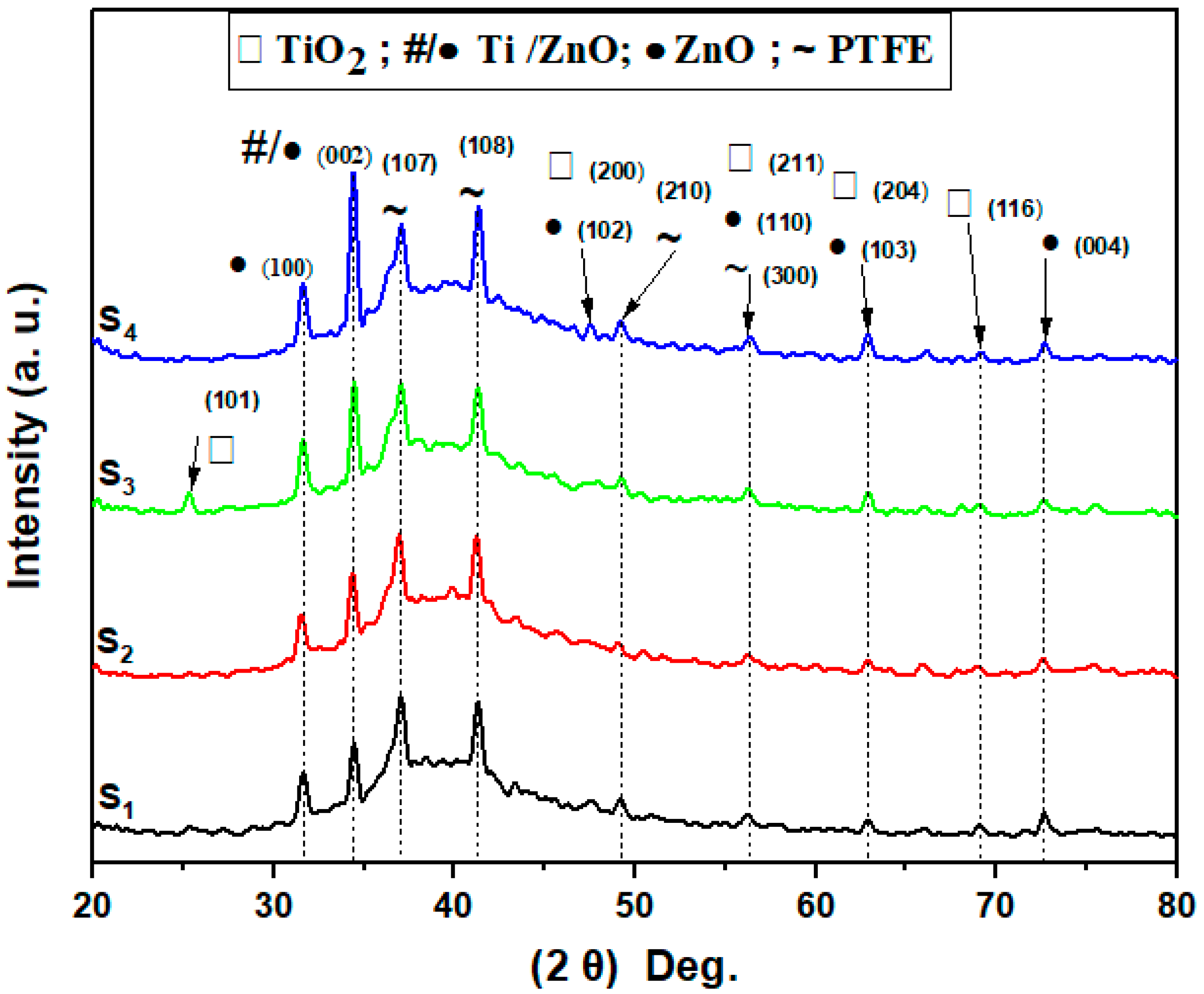
Figure 4 shows the AFM results taken at a topographical scan area of 10 × 10 µm2. First, no cracks were detected in the samples. Concerning each sample, it was observed that the direct addition of the TiO2 ratio was directly proportional to the increase in the grooves generated during doping. The root-mean-square surface roughness (Rq) in Table 2 quantitively describes the effect of the TiO2 percentage on the surface topography. Further, the increase in photocatalyst ratios during sample synthesis and its effect can be observed in the lateral lines where the variation in height increases with more peak–valley points. Consequentially, the topographies support the abovementioned FESEM and EDX results. Rough surfaces are desirable because they enhance multiple light reflections from the samples. Moreover, the absorptions and tandem reflections of radiation increase based on the effect of the wavelength accompanying the measurement, whereas vertical or patterned surfaces are necessary for the entire retention of incident light [46,47,48].

3.4. XRD Analysis

Figure 5 elucidates the XRD patterns of the nanocomposite on the PTFE substrates for all four samples. The patterns show peaks of ZnO, (Ti/ZnO) NRs in wurtzite structures, TiO2/ZnO, and TiO2 heterostructure peaks on all samples. The TiO2 peaks for the final two samples were shaped at jagged, indiscriminate, and diverse keel angles [25,45,49,50,51,52]. These peaks have been confirmed by relevant standard calibrations in agreement with JCPDS card number 01-080-0074. Equations (10)–(12) were used for the computation of crystalline size (D), lattice constant (c), and strain along the c-axis ( ε z z % ) , respectively [1,6,53].
D = 0.9 λ   β cos θ
c = λ sin θ
ε z z % = c c 0 c 0 %
where c 0 is the standard lattice constant (unstrained), λ is the wavelength of the X-ray source (λcu = 0.1541 nm), β is the full width at half maximum (FWHM), and θ is the peak angle position obtained by X-ray apparatus. The c 0 was enrolled as a function of semiconductors, where c 0 (ZnO) = 0.52098 nm; c 0 (Ti/ZnO) = 0.52125 nm [25,54]. The acquired data were tabulated in Table 3 for samples S1, S2, S3, and S4 correlated by the synthesis ratios of TiO2:ZnO as 1:7, 1:3, 3:5, and 1:1, respectively.
For the nanocomposites on PTFE substrates, the first peak is at around 31.25°. The c is found to be greater than c0, indicating that the axial structural frame is distorted (εzz% > 1%), which could be attributed to the tensile stress and partial incorporations between units of ZnO crystals. The second peak has εzz% = −0.12%, indicating compressive stress due to the high quality of the wurtzite structure. The distinguishable pointer arises from a narrow FWHM, which confirms that the Ti/ZnO incorporative crystalline is verified [1,6,55]. The third peak reveals the angle between hkl planes (∅) of TiO2 and ZnO at 30°. A relatively large D may indicate that TiO2 is constructed above and incorporated into ZnO NRs (TiO2/ZnO), which produces deformation in ZnO NRs of TiO2. This finding was supported by the value of εzz% (ZnO) = −36.8%, which was predicted owing to the agglomerated TiO2 affecting the quality of the wurtzite structure of ZnO NRs [50,52,56,57]. The interpreted formation of the fourth peak is similar to that shown in the third peak, except that the value is small and there is a sharp decrease in the D value. For both the fifth and seventh peaks, D values increased due to TiO2 agglomeration growth. At the eighth peak, ∅ = 63°, however, D shows the highest value, which is likely to be caused by the large TiO2 agglomerations that influence the εzz% value, as described at the third peak [25,50,52,56]. For the sixth peak, both D and εzz% (ZnO) were the smallest, which may be attributed to ZnO nanoparticles [58,59].

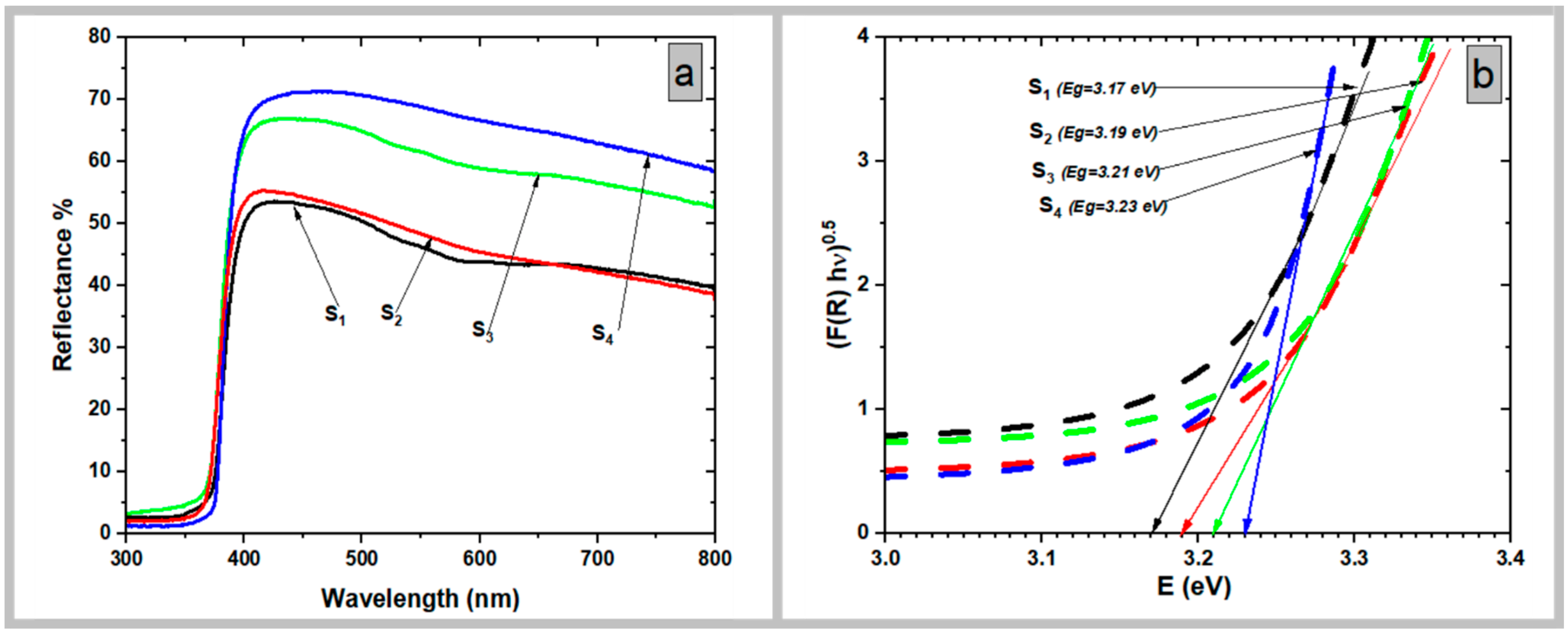
3.5. UV–Vis Diffuse Reflectance Spectra

Figure 6a displays the diffused reflectance spectra for the nanocomposites grown at ratios of TiO2 to ZnO of 1:7, 1:3, 3:5, and 1:1, representing samples S1, S2, S3, and S4, sequentially. The wavelength spectra were varied within the range of 300 to 800 nm. Based on the increasing ratio of TiO2, it was found that the sharp reflectance edges were slightly variegated, which implies the incorporation of the triple and quaternary of Ti ions within ZnO NRs, as well as the TiO2 enhancement, which causes the increase in reflectivity. The dopant addition process has arranged for the enhancement of oxygen vacancies, which may contribute to the raising of curves (i.e., reflectance enlargement axis). It is believed that the texture of PTFE also contributes to the photonic interaction due to the intrinsic optical characteristics of Teflon, such as refractive index, fluorine atom negativity, and capacitance parameter related to carbon [23]. The apparent effect of altitude on the reflectivity curve of sample S1 could be due to either the surface reflectivity contribution of the substrate or associated with the indirect transfer of photoelectrons in the nanocomposite [60,61,62,63].
Diffuse reflectance spectra and the well-known Kubelka–Munk function ( F R ) were used to calculate the bandgap energies. This function transforms reflectance ( R ) data to the absorption coefficient, as described by Equations (13)–(15) [64]:
F R = 1 R 2 2 R = K S
The scattering and absorption Kubelka–Munk coefficients were denoted by S and K , respectively. The absorption coefficient could be comparable to the Kubelka–Munk function in the following sense of Equation (14):
K = SF(R)
Hence, the bandgap energy is computed by the Tauc relation in Equation (15):
F R h v = A h v E g n
where n is equal to 2 for indirect band gap materials, v is the light frequency, and A is a proportionality constant. Extrapolating the ( F R h v )1/2 against the energy E e V plot to the axis cut-off yields the band gap. From Figure 6b, the expectation values of the band gap energy of the samples using diffuse reflectance spectra data and the Kubelka–Munk equation are 3.17 eV, 3.19 eV, 3.21 eV, and 3.23 eV for the samples S1, S2, S3, and S4, respectively. These values, in particular, differed around the typical bandgap energy values of TiO2 and ZnO. In this case, they may be interpreted from two logical probabilities: the first is due to doping influences resulting from enhanced photocatalyst synthesis ratios [6], and the second is ascribed to the locations of interstitial edges and internal commutative levels for TiO2/ZnO that correlate to heterostructure straddling (type-I) and staggered (type-II). For these reasons, the new band gap values could boost the potential of transferring photoelectrons through them, which affects the optical properties of the nanocomposites [60]. Although ZnO has been reported in the literature as a direct band gap semiconductor material, some studies reported indirect band gaps significantly if the ZnO was affected by external influencers such as doping. Based on the obtained UV–Vis data, the line fitting preferred an indirect band gap situation [60,65].

3.6. FTIR Analysis

Figure 7 shows the FTIR spectra and functional groups of the grown nanocomposites on PTFE substrates calibrated on the most vital significant vibrational phonon bonds. The vibrational phonon bonds were detailed in cm−1 units, where sample (S1) contained Ti–O at 448 and 480 cm−1, Zn–O at 379 and 415 cm−1, and Ti–O–Ti at 534 cm−1. For sample (S2), the vibrational phonon bonds included Ti–O at 448 cm−1, Zn–O at 379 and 560 cm−1, Ti–O–Ti at 534 cm−1, and TiO2–ZnO at 485 and 892 cm−1. Sample (S3) comprised Ti–O at 448 and 480 cm−1, Zn–O at 380 and 420 cm−1, Ti–O–Ti at 534 cm−1, Ti–O–O at 690 cm−1, and TiO2–ZnO at 890 and 1600 cm−1. Sample (S4) embraced Ti–O at 448 and 480 cm−1, Zn–O at 415 and 379 cm−1, Ti–O–Ti at 534 cm−1, and TiO2–ZnO at set (485, 892, 1081, and 1412 cm−1). However, the PTFE substrates have fixed peaks at around 1155 and 1215 cm−1, which may be attributed to non-vibration bonding in the IR range, emphasizing the IR non-absorber C–F surface [7,55,63,66,67,68,69,70,71,72]. It is observed that chemical bonding peaks varied through the TiO2:ZnO ratios of the mentioned samples, particularly the diverse vibrational peaks of TiO2–ZnO.
As can be referred from Table 1, the atomic relative ratios of Ti/O, Zn/O, and Ti/Zn are directly proportional to the applicable ratios of the TiO2 during the growth process. Based on the occurrences of IR vibration peaks, Table 4 demonstrates that the Ti/O result of each sample as a comparison was a low fraction of one, which indicates the possibility of increasing the Ti–O and Ti–O–Ti chemical bonds of the grown nanocomposites. This may be attributed to the abundance of oxygen and postulates of oxygen chemical joints. Zn/O may give oxygen vacancy variation, which supports optical properties and Zn–O bonds. In addition, the increasing values of Ti/Zn indicate successful doping, which is reported to enhance the photocatalytic performance of optoelectronics devices [3,26,45,73].

3.7. Characteristics of the UV Photodetectors

This section discusses the photoresponse and current–voltage properties of photodetector devices fabricated using S1, S2, S3, and S4, which CBD synthesized on the PTFE substrates. The photodetectors have an MSM structure with an IDE electrode printed on the samples that have been grown previously. The photodetectors were labeled with the same labels used for the grown samples (S1 = 1:7), (S2 = 1:3), (S3 = 3:5), and (S4 = 1:1).

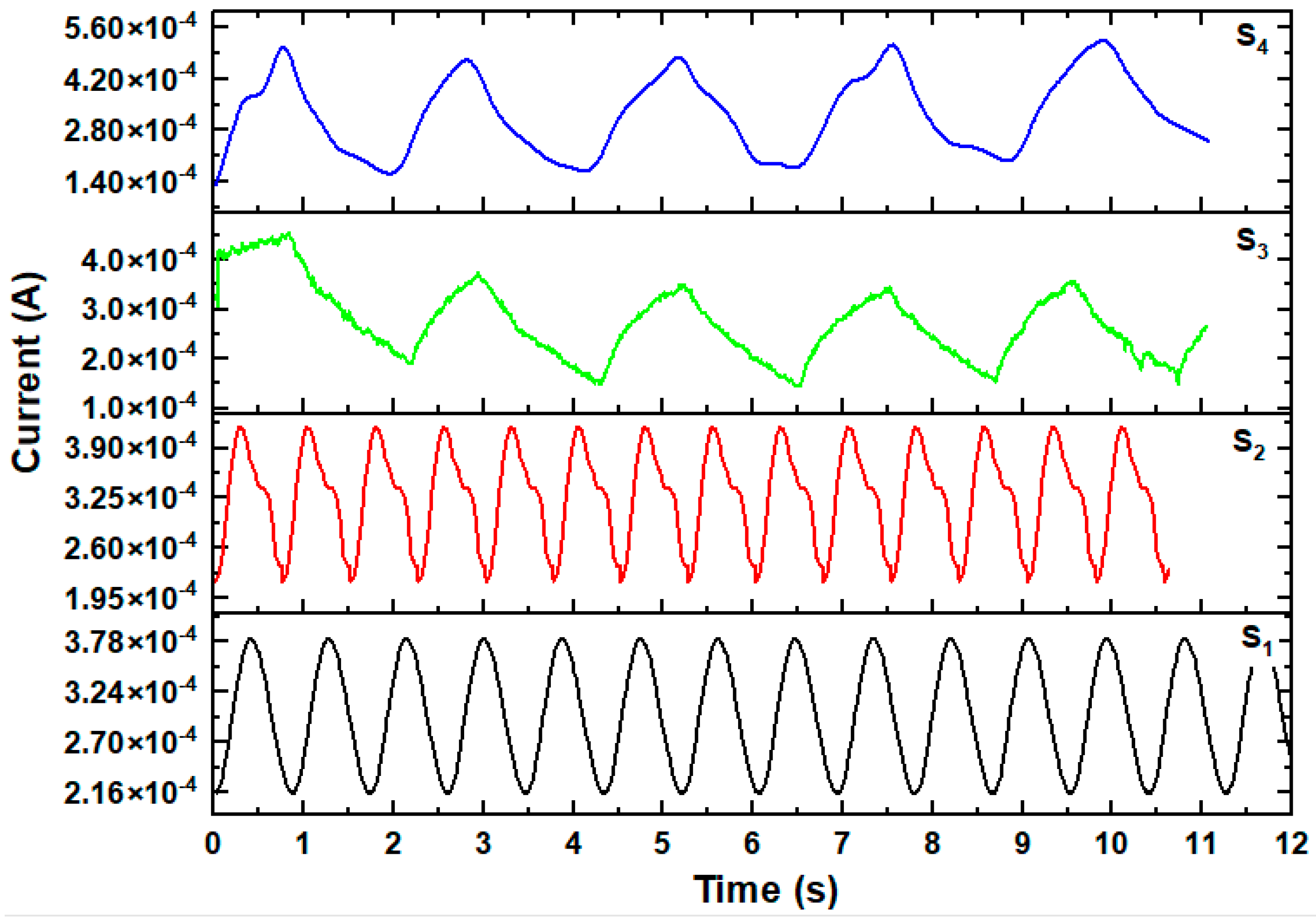
3.7.1. Photo-Response Properties

Figure 8 elucidates the current-to-time (I–t) response in the switched on/off states of UV light of 365 nm wavelength, 2.83 mW/cm2 power, and +3 V bias voltage for the S1, S2, S3, and S4 photodetector devices in ascending frames. The photocurrent curves of the devices began to vary and grow exponentially at the UV-ON status, from a semi-sinusoidal wave to a semi-sawtooth wave gradually, followed by an exponential reduction with the light at the UV-OFF status. The areas under photocurrent curves increased ascendingly, which could indicate gradual growth in the photocarrier charges per device. For example, photogenerated electron–hole pairs proliferated, increasing the likelihood of non-recombination [74]. The photodetectors based on the Ag IDE electrodes performed well with reproducibility and repeatability of photocurrent during the light on-off cycling. This is attributed to the fact that after the light is turned out, the photocurrent remains in each device for a long time (decay time) in direct proportion to the raised time. According to surface adsorption/desorption processes, the delayed decay time may result from the slow photocarrier relaxation behavior [75]. However, the characteristics of each device’s obtained raise and decay times exhibit outstanding reproducibility with slight variance, proving its good stability. In order to determine how quickly the detector reacts to a rapidly changing optical input, the photocurrent rise and fall times are investigated. The rise time (τr) is the amount of time required to increase the photocurrent from 10% to 90% of its maximum value (τr = τ90%τ10%), and the decay time (τd) is the amount of time required to decrease the photocurrent from 90% to 10% of its maximum value (τd = τ10%τ90%), where τ10% and τ90% are the amounts of time spent corresponding to the saturated photocurrent values of 10% and 90%, respectively [76].
The five significant metrics of photodetector devices are responsivity ( R ), photosensitivity ( S ), gain ( G ), detectivity ( D ), and external quantum efficiency ( E Q E ), determined using Equations (16)–(21), respectively [25,76,77].
I p h = I L I d
R = I p h A   P i n
S = I p h I d × 100 %
G = I L   I d
D = R A 2   e   I d
E Q E = h c R e   λ × 100 %
where I p h , I L ,   I d , A, P i n , h, e, c, and λ are the photocurrent, light current, dark current, illuminated area, incident optical power per unit area, Plank’s constant, unit of elementary charge, speed of light, and incident light wavelength, sequentially. Table 5 depicts the main electrical specifications of the photodetector devices fabricated using samples S1, S2, S3, and S4. The increase in the electrical properties could be attributed to the photocatalytic synthesis ratios [38] and the thickness of the precipitate, which affects the boost release of the photoelectrons [78]. It should be noted that frequently exposing the devices to light had no impact on the performance of the photodetectors, indicating excellent repeatability. Additionally, once the light was switched off for a while, the photocurrent persisted in each device for a period of time directly proportional to the doping concentration.
Table 6 compares the results obtained in this work, which are illustrated in Figure 8 and Table 5, to values obtained from the literature. However, there were several differences between the parameters in the literature and those in this study, such as those relevant to synthesis methods, electrode contact types, UV-exposed areas, self-constants of UV sources, and bias voltages. Accordingly, it can be demonstrated that the devices in this work have almost preferable UV detection data to the results found in the literature.

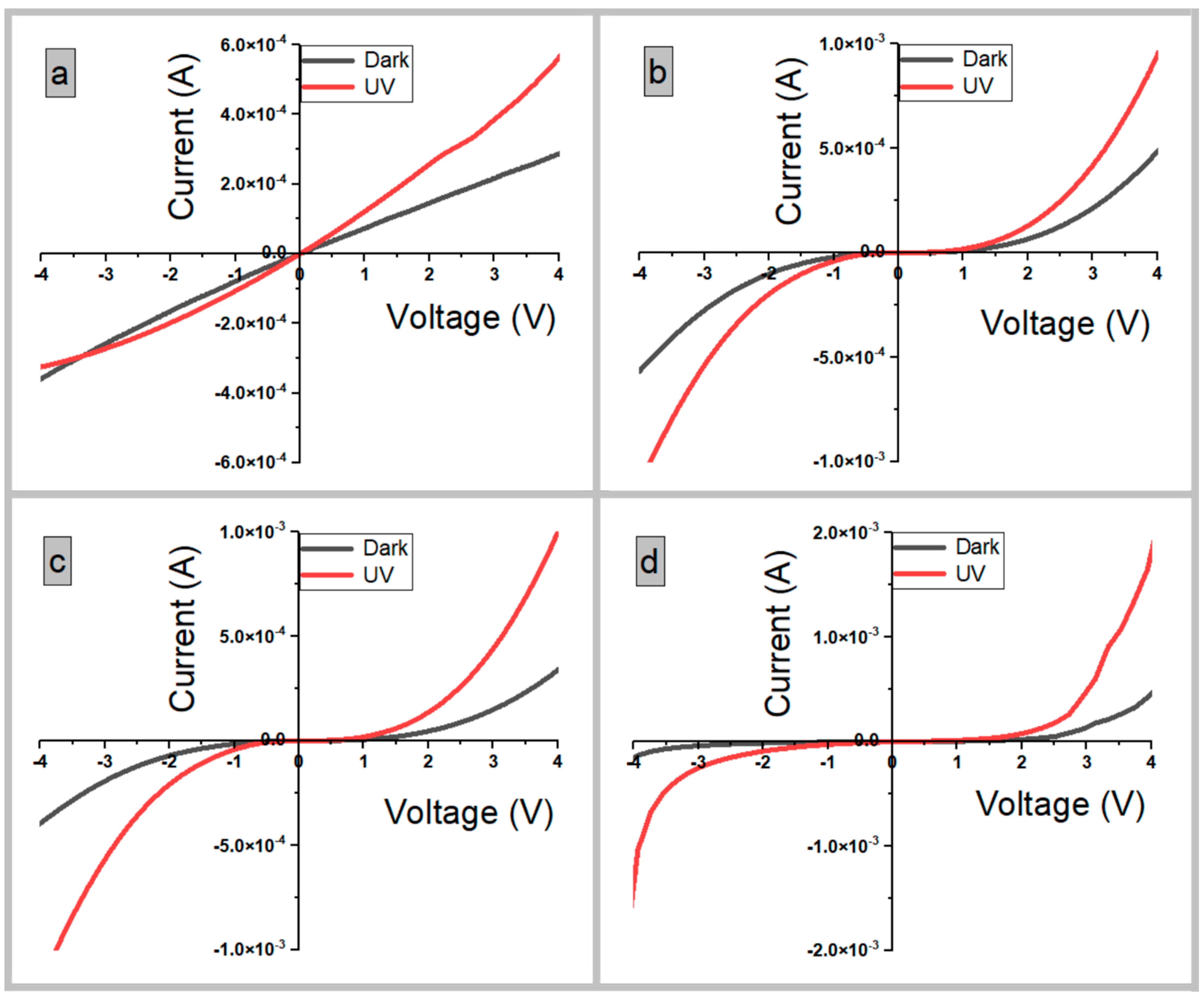
3.7.2. Current–Voltage Properties

Figure 9 elucidates the obtained results of current–voltage (I–V) characteristic curves of each photodetector device in the dark and UV illuminance mode using a UV source with the parameters of 365 nm and 2.83 mW/cm2 along an applied bias voltage ranging from −4V to +4V. The asymmetrical nonlinear I–V curves measured from the device fabricated using sample S1 appeared semi-ohmic, especially when exposed to UV light. The behavior of the asymmetric nonlinear I–V curve of the following three devices, whether in the dark or under UV irradiation at normal ambient conditions, indicated the formation of Schottky barrier junctions between the nanocomposite surface and the Ag electrodes [84]. This could be attributed to the Schottky contacts formed between the TiO2/ZnO heterojunction and the Ag electrode by reason of the work functions for each undoped ZnO, TiO2, and Ag range, which were individually recorded as 4.2 eV, 4.5 eV, and around 4.26 eV to 4.74 eV, respectively. The decrease in the work function could be exhibited by the occurrence of doping for ZnO and TiO2 in addition to their roles in forming the shared heterojunction. The changes in the work function of Ag while interfacing with the nanocomposite could be responsible for shifting the curves from semi-ohmic to asymmetric nonlinear Schottky junction, which was previously reported in the literature [85,86,87].
Further, I–V measurements of all the devices exhibited good reproducibility and were realized to be relatively increasing due to the direct proportion of photocatalytic synthesis ratios, which indicates their quality. For each photodetector device, the IL was comparatively greater than the Id at the forward bias voltage, incrementally in an exponential frame per device, while they were arising out in curves contrastingly at the backward bias voltage range. In these cases, the logical interpretation of the Id charge carrier mechanisms was related to the captured free electrons by the adsorbed oxygen molecules linked with the nanocomposites [88]; whereas the IL leads to the generation of photo-excited electron-hole pairs, the migrated holes combine with oxygen anions, resulting in the desorption of oxygen molecules from the surface [89]. This process results in an increment in the free carrier charges. Hence, IL increased upon light illumination compared to the Id that resulted from heterostructure forms associated with Ti-doped ZnO thin films such as Ti:TiO2/ZnO. It was also noted that the influence of Ti as a dopant depended on the increasing ratio of TiO2 and that the proposed synthesization procedures and electrode-type deposition impacted the measured values of Id and IL.

4. Conclusions

Ti:TiO2/ZnO nanocomposites have been synthesized on PTFE substrates by employing the CBD method in a thermodynamically closed system. The synthesis process of the composite involved volumetric control ratios between TiO2 nanofluid and ZnO precursor in order to enhance the photocatalytic properties of ZnO NRs. FESEM and EDX analysis revealed that the structure of the nanorods and the elemental atomic percentages were different based on the TiO2:ZnO ratio. The 2D and 3D topography images obtained by AFM showed a roughness increase with an increase in the TiO2 doping concentration from 66.8 nm to 107 nm. The XRD spectra revealed numerous distinguishable peaks for the nanocomposites grown on the PTFE substrates, particularly the unified wurtzite structure dopant peak (002). The UV–Vis reflectance curves illustrated bandgap variations from 3.17 eV to 3.23 eV (interfacial bandgaps of TiO2 and ZnO). The phonon vibrations from FTIR spectra revealed the presence of Ti–O and Zn–O bonds. Ag electrodes were deposited on the top of the grown TFs to serve as photodetectors in an MSM structure. It was worth noting that the influence of TiO2 contents in ZnO produced noticeable improvements in the photodetector’s electrical characteristics when compared to the literature. The nano-heterostructure might, as a result, indicate significant potential for optoelectronic applications.

Author Contributions

Conceptualization, Y.S.M.E.; Data curation, Y.S.M.E.; Formal analysis, Y.S.M.E.; Funding acquisition, M.R.H.; Methodology, Y.S.M.E.; Project administration, M.R.H.; Resources, M.R.H. and M.M.H.; Supervision, M.R.H. and M.M.H.; Validation, M.R.H., M.M.H. and A.A.; Writing—original draft, Y.S.M.E.; Writing—review and editing, M.R.H., M.M.H. and A.A. All authors have read and agreed to the published version of the manuscript.

Funding

This research was funded by the Ministry of Higher Education Malaysia, grant number FRGS/1/2020/STG07/USM/02/10. The APC was funded by Universiti Sains Malaysia.

Institutional Review Board Statement

Not applicable.

Informed Consent Statement

Not applicable.

Data Availability Statement

Not applicable.

Acknowledgments

The authors would like to acknowledge the funding by the Ministry of Higher Education Malaysia for the Fundamental Research Grant Scheme with Project Code: FRGS/1/2020/STG07/USM/02/10. In addition, extended appreciation to the staff of Nano-Optoelectronics Research and Technology Laboratory (NORLab), School of Physics, Universiti Sains Malaysia.

Conflicts of Interest

The authors declare no conflict of interest.

References

  1. Shaheera, M.; Girija, K.G.; Kaur, M.; Geetha, V.; Debnath, A.K.; Vatsa, R.K.; Muthe, K.P.; Gadkari, S.C. Elucidation of Structural, Morphological, Optical and Photoluminescence Properties of Single and (In, Ga) Co-Doped ZnO Nanocrystalline Thin Films. Bull. Mater. Sci. 2019, 42, 266. [Google Scholar] [CrossRef]
  2. Epie, E.N.; Chu, W.K. Ionoluminescence Study of Zn—and O—Implanted ZnO Crystals: An Additional Perspective. Appl. Surf. Sci. 2016, 371, 28–34. [Google Scholar] [CrossRef]
  3. Saikia, L.; Bhuyan, D.; Saikia, M.; Malakar, B.; Dutta, D.K.; Sengupta, P. Photocatalytic Performance of ZnO Nanomaterials for Self Sensitized Degradation of Malachite Green Dye under Solar Light. Appl. Catal. A Gen. 2015, 490, 42–49. [Google Scholar] [CrossRef]
  4. Zhang, Q.; Li, C. TiO2 Coated Zno Nanorods by Mist Chemical Vapor Deposition for Application as Photoanodes for Dye-Sensitized Solar Cells. Nanomaterials 2019, 9, 1339. [Google Scholar] [CrossRef] [PubMed]
  5. Mi, Y.; Weng, Y. Band Alignment and Controllable Electron Migration between Rutile and Anatase TiO2. Sci. Rep. 2015, 5, 11482. [Google Scholar] [CrossRef] [PubMed]
  6. Bidier, S.A.; Hashim, M.R.; Bououdina, M. Structural and Optical Characteristics of Ti-Doped ZnO Nanorods Deposited by Simple Chemical Bath Deposition. J. Mater. Sci. Mater. Electron. 2017, 28, 11178–11185. [Google Scholar] [CrossRef]
  7. Ilkhechi, N.N.; Mozammel, M.; Khosroushahi, A.Y. Antifungal Effects of ZnO, TiO2 and ZnO-TiO2 Nanostructures on Aspergillus Flavus. Pestic. Biochem. Physiol. 2021, 176, 104869. [Google Scholar] [CrossRef]
  8. Sahrin, N.T.; Nawaz, R.; Chong, F.K.; Lee, S.L.; Wirzal, M.D.H. Current Perspectives of Anodized TiO2 Nanotubes towards Photodegradation of Formaldehyde: A Short Review. Environ. Technol. Innov. 2021, 22, 101418. [Google Scholar] [CrossRef]
  9. Gupta, T.; Samriti; Cho, J.; Prakash, J. Hydrothermal Synthesis of TiO2 Nanorods: Formation Chemistry, Growth Mechanism, and Tailoring of Surface Properties for Photocatalytic Activities. Mater. Today Chem. 2021, 20, 100428. [Google Scholar] [CrossRef]
  10. Seshan, K. Handbook of Thin Film Deposition Techniques Principles, Methods, Equipment and Applications, 2nd ed.; CRC Press: Boca Raton, FL, USA, 2002; ISBN 9780429076749. [Google Scholar]
  11. Enríquez, J. Influence of the Thickness on Structural, Optical and Electrical Properties of Chemical Bath Deposited CdS Thin Films. Sol. Energy Mater. Sol. Cells 2003, 76, 313–322. [Google Scholar] [CrossRef]
  12. Lopez Garcia, A.J.; Sico, G.; Montanino, M.; Defoor, V.; Pusty, M.; Mescot, X.; Loffredo, F.; Villani, F.; Nenna, G.; Ardila, G. Low-temperature Growth of Zno Nanowires from Gravure-Printed Zno Nanoparticle Seed Layers for Flexible Piezoelectric Devices. Nanomaterials 2021, 11, 1430. [Google Scholar] [CrossRef]
  13. Kumar, A.; Kumar, M.; Bhatt, V.; Mukherjee, S.; Kumar, S.; Sharma, H.; Yadav, M.K.; Tomar, S.; Yun, J.H.; Choubey, R.K. Highly Responsive and Low-Cost Ultraviolet Sensor Based on ZnS/p-Si Heterojunction Grown by Chemical Bath Deposition. Sens. Actuators A Phys. 2021, 331, 112988. [Google Scholar] [CrossRef]
  14. Poornajar, M.; Marashi, P.; Haghshenas Fatmehsari, D.; Kolahdouz Esfahani, M. Synthesis of ZnO Nanorods via Chemical Bath Deposition Method: The Effects of Physicochemical Factors. Ceram. Int. 2016, 42, 173–184. [Google Scholar] [CrossRef]
  15. Zhang, Z.; Hu, Y.; Qin, F.; Ding, Y. DC Sputtering Assisted Nano-Branched Core-Shell TiO 2 /ZnO Electrodes for Application in Dye-Sensitized Solar Cells. Appl. Surf. Sci. 2016, 376, 10–15. [Google Scholar] [CrossRef]
  16. Pawar, V.; Kumar, M.; Dubey, P.K.; Singh, M.K.; Sinha, A.S.K.; Singh, P. Influence of Synthesis Route on Structural, Optical, and Electrical Properties of TiO2. Appl. Phys. A Mater. Sci. Process. 2019, 125, 657. [Google Scholar] [CrossRef]
  17. Kolodziejczak-Radzimska, A.; Jesionowski, T. Zinc Oxide—From Synthesis to Application: A Review. Materials 2014, 7, 2833–2881. [Google Scholar] [CrossRef]
  18. Muhammad, A.; Mohammad, S.M.; Hassan, Z.; Rajamanickam, S.; Abed, S.M.; Ashiq, M.G.B. Fabrication of Fluorine and Silver Co-Doped ZnO Photodetector Using Modified Hydrothermal Method. Microelectron. Int. 2022, 40. [Google Scholar] [CrossRef]
  19. Wisz, G.; Sawicka-Chudy, P.; Wal, A.; Potera, P.; Bester, M.; Płoch, D.; Sibiński, M.; Cholewa, M.; Ruszała, M. TiO2:ZnO/CuO Thin Film Solar Cells Prepared via Reactive Direct-Current (DC) Magnetron Sputtering. Appl. Mater. Today 2022, 29, 101673. [Google Scholar] [CrossRef]
  20. Huang, J.Y.; Wang, Y.; Fei, G.T.; Xu, S.H.; Zeng, Z.; Wang, B. TiO2/ZnO Double-Layer Broadband Antireflective and Down-Shifting Coatings for Solar Applications. Ceram. Int. 2022. [Google Scholar] [CrossRef]
  21. Alfakes, B.; Garlisi, C.; Villegas, J.; Al-Hagri, A.; Tamalampudi, S.; Rajput, N.S.; Lu, J.Y.; Lewin, E.; Sá, J.; Almansouri, I.; et al. Enhanced Photoelectrochemical Performance of Atomic Layer Deposited Hf-Doped ZnO. Surf. Coatings Technol. 2020, 385, 125352. [Google Scholar] [CrossRef]
  22. Ahmad, H.; Naderi, N. Enhanced Optoelectrical Performance of Ultraviolet Detectors Based on Self-Assembled Porous Zinc Oxide Nanostructures. Ceram. Int. 2022. [Google Scholar] [CrossRef]
  23. Dhanumalayan, E.; Joshi, G.M. Performance Properties and Applications of Polytetrafluoroethylene (PTFE)—A Review. Adv. Compos. Hybrid Mater. 2018, 1, 247–268. [Google Scholar] [CrossRef]
  24. Edinger, S.; Bansal, N.; Bauch, M.; Wibowo, R.A.; Hamid, R.; Trimmel, G.; Dimopoulos, T. Comparison of Chemical Bath-Deposited ZnO Films Doped with Al, Ga and In. J. Mater. Sci. 2017, 52, 9410–9423. [Google Scholar] [CrossRef]
  25. Farhat, O.F.; Halim, M.M.; Ahmed, N.M.; Oglat, A.A.; Abuelsamen, A.A.; Bououdina, M.; Qaeed, M.A. A Study of the Effects of Aligned Vertically Growth Time on ZnO Nanorods Deposited for the First Time on Teflon Substrate. Appl. Surf. Sci. 2017, 426, 906–912. [Google Scholar] [CrossRef]
  26. Farhat, O.F.; Halim, M.M.; Abdullah, M.J.; Ali, M.K.M.; Ahmed, N.M.; Allam, N.K. Growth of Vertically Aligned ZnO Nanorods on Teflon as a Novel Substrate for Low-Power Flexible Light Sensors. Appl. Phys. A Mater. Sci. Process. 2015, 119, 1197–1201. [Google Scholar] [CrossRef]
  27. Farhat, O.F.; Halim, M.M.; Ahmed, N.M.; Qaeed, M.A. ZnO Nanofiber (NFs) Growth from ZnO Nanowires (NWs) by Controlling Growth Temperature on Flexible Teflon Substrate by CBD Technique for UV Photodetector. Superlattices Microstruct. 2016, 100, 1120–1127. [Google Scholar] [CrossRef]
  28. Ade, R.; Kumar, S.S.; Valanarasu, S.; Kumar, S.S.; Sasikumar, S.; Ganesh, V.; Bitla, Y.; Algarni, H.; Yahia, I.S. Enhanced Optoelectronic Properties of Ti-Doped ZnO Nanorods for Photodetector Applications. Ceram. Int. 2021, 47, 24031–24038. [Google Scholar] [CrossRef]
  29. Dao, T.D.; Dang, C.T.T.; Han, G.; Hoang, C.V.; Yi, W.; Narayanamurti, V.; Nagao, T. Chemically Synthesized Nanowire TiO2/ZnO Core-Shell P-N Junction Array for High Sensitivity Ultraviolet Photodetector. Appl. Phys. Lett. 2013, 103, 193119. [Google Scholar] [CrossRef]
  30. Shaikh, S.K.; Ganbavle, V.V.; Inamdar, S.I.; Rajpure, K.Y. Multifunctional Zinc Oxide Thin Films for High-Performance UV Photodetectors and Nitrogen Dioxide Gas Sensors. RSC Adv. 2016, 6, 25641–25650. [Google Scholar] [CrossRef]
  31. Nguyen, X.H.; Luong, H.N.; Pham, H.A.; Nguyen, N.M.; Dang, V.Q. Visible Photodetector Based on Transition Metal-Doped ZnO NRs/PEDOT:PSS Hybrid Materials. RSC Adv. 2021, 11, 36340–36347. [Google Scholar] [CrossRef]
  32. Zhou, M.; Wu, B.; Zhang, X.; Cao, S.; Ma, P.; Wang, K.; Fan, Z.; Su, M. Preparation and UV Photoelectric Properties of Aligned ZnO-TiO2and TiO2-ZnO Core-Shell Structured Heterojunction Nanotubes. ACS Appl. Mater. Interfaces 2020, 12, 38490–38498. [Google Scholar] [CrossRef] [PubMed]
  33. Alwadai, N.; Mitra, S.; Hedhili, M.N.; Alamoudi, H.; Xin, B.; Alaal, N.; Roqan, I.S. Enhanced-Performance Self-Powered Solar-Blind UV-C Photodetector Based on N-ZnO Quantum Dots Functionalized by P-CuO Micro-Pyramids. ACS Appl. Mater. Interfaces 2021, 13, 33335–33344. [Google Scholar] [CrossRef] [PubMed]
  34. Ali, H.M.; Babar, H.; Shah, T.R.; Sajid, M.U.; Qasim, M.A.; Javed, S. Preparation Techniques of TiO2 Nanofluids and Challenges: A Review. Appl. Sci. 2018, 8, 587. [Google Scholar] [CrossRef]
  35. Tiple, A.; Sinhmar, P.S.; Gogate, P.R. Improved Direct Synthesis of TiO2 Catalyst Using Sonication and Its Application for the Desulfurization of Thiophene. Ultrason. Sonochem. 2021, 73, 105547. [Google Scholar] [CrossRef] [PubMed]
  36. Sánchez-Tovar, R.; Blasco-Tamarit, E.; Fernández-Domene, R.M.; Villanueva-Pascual, M.; García-Antón, J. Electrochemical Formation of Novel TiO2-ZnO Hybrid Nanostructures for Photoelectrochemical Water Splitting Applications. Surf. Coat. Technol. 2020, 388, 125605. [Google Scholar] [CrossRef]
  37. Truong, D.C.; Thaowonkaew, S.; Muthitamongkol, P.; Horprathum, M.; Kumar, M.; Le, T.B.N.; Pham, A.T.T.; Seetawan, T.; Vora-ud, A.; Phan, T.B. Relaxation of Residual Stress-Controlled Thermopower Factor in Transparent-Flexible Ti-Doped ZnO Thin Films. Ceram. Int. 2022, 48, 2605–2613. [Google Scholar] [CrossRef]
  38. Fu, R.; Wang, Q.; Gao, S.; Wang, Z.; Huang, B.; Dai, Y.; Lu, J. Effect of Different Processes and Ti/Zn Molar Ratios on the Structure, Morphology, and Enhanced Photoelectrochemical and Photocatalytic Performance of Ti3+ Self-Doped Titanium-Zinc Hybrid Oxides. J. Power Sources 2015, 285, 449–459. [Google Scholar] [CrossRef]
  39. Na, S.; Seo, S.; Lee, H. Recent Developments of Advanced Ti3+-Self-Doped TiO2 for Efficient Visible-Light-Driven Photocatalysis. Catalysts 2020, 10, 679. [Google Scholar] [CrossRef]
  40. Watanabe, H.; Yamada, N.; Okaji, M. Linear Thermal Expansion Coefficient of Silicon from 293 to 1000 K. Int. J. Thermophys. 2004, 25, 221–236. [Google Scholar] [CrossRef]
  41. Lima, M.F.S.; Villeti, M.; Samios, D. Thermodynamical Behaviour of Deformed Semicrystalline Polymers in Temperatures between Tg and Tm. J. Polym. Eng. 1997, 17, 75–94. [Google Scholar] [CrossRef]
  42. Jamil, A.; Fareed, S.; Tiwari, N.; Li, C.; Cheng, B.; Xu, X.; Rafiq, M.A. Effect of Titanium Doping on Conductivity, Density of States and Conduction Mechanism in ZnO Thin Film. Appl. Phys. A Mater. Sci. Process. 2019, 125, 238. [Google Scholar] [CrossRef]
  43. Hsiang, H.I.; Liu, Y.L. Electrical Properties of Copper and Titanium-Codoped Zinc Ferrites. J. Alloys Compd. 2009, 472, 516–520. [Google Scholar] [CrossRef]
  44. Lou, Z.; Deng, J.; Wang, L.; Wang, R.; Fei, T.; Zhang, T. A Class of Hierarchical Nanostructures: ZnO Surface-Functionalized TiO 2 with Enhanced Sensing Properties. RSC Adv. 2013, 3, 3131–3136. [Google Scholar] [CrossRef]
  45. Tayel, A.; Ramadan, A.R.; El Seoud, O.A. Titanium Dioxide/graphene and Titanium Dioxide/graphene Oxide Nanocomposites: Synthesis, Characterization and Photocatalytic Applications for Water Decontamination. Catalysts 2018, 8, 491. [Google Scholar] [CrossRef]
  46. Butalid, R.J.B.; Cristobal, A.P.S.; Montallana, A.D.S.; Vasquez, M.R. Stability of TiO2 -Coated ZnO Photocatalytic Thin Films for Photodegradation of Methylene Blue. J. Vac. Sci. Technol. B 2020, 38, 62205. [Google Scholar] [CrossRef]
  47. Mokkapati, S.; Beck, F.J.; De Waele, R.; Polman, A.; Catchpole, K.R. Resonant Nano-Antennas for Light Trapping in Plasmonic Solar Cells. J. Phys. D Appl. Phys. 2011, 44, 185101. [Google Scholar] [CrossRef]
  48. Martínez, L.; García-Salgado, G.; Morales-Morales, F.; Campillo, B.; Hernández, A.G.; Karthik, T.V.K.; Jiménez-Vivanco, M.R.; Campos-álvarez, J. Zno Films Incorporation Study on Macroporous Silicon Structure. Materials 2021, 14, 3697. [Google Scholar] [CrossRef]
  49. Al-Ruqeishi, M.S.; Mohiuddin, T. Growth of Single-Sided ZnO nanocombs/ML Graphene Heterostructures. Arab. J. Chem. 2019, 12, 2774–2781. [Google Scholar] [CrossRef]
  50. Praveen, P.; Viruthagiri, G.; Mugundan, S.; Shanmugam, N. Structural, Optical and Morphological Analyses of Pristine Titanium Di-Oxide Nanoparticles—Synthesized via Sol-Gel Route. Spectrochim. Acta Part A Mol. Biomol. Spectrosc. 2014, 117, 622–629. [Google Scholar] [CrossRef]
  51. Surmenev, R.A.; Surmeneva, M.A.; Grubova, I.Y.; Chernozem, R.V.; Krause, B.; Baumbach, T.; Loza, K.; Epple, M. RF Magnetron Sputtering of a Hydroxyapatite Target: A Comparison Study on Polytetrafluorethylene and Titanium Substrates. Appl. Surf. Sci. 2017, 414, 335–344. [Google Scholar] [CrossRef]
  52. Dobromir, M.; Konrad-Soare, C.T.; Stoian, G.; Semchenko, A.; Kovalenko, D.; Luca, D. Surface Wettability of Zno-Loaded TiO2 Nanotube Array Layers. Nanomaterials 2020, 10, 1901. [Google Scholar] [CrossRef] [PubMed]
  53. Aguilar-Marín, P.; Angelats-Silva, L.; Noriega-Diaz, E.; Chavez-Bacilio, M.; Verde-Vera, R. Understanding the Phenomenon of X-ray Diffraction by Crystals and Related Concepts. Eur. J. Phys. 2020, 41, 045501. [Google Scholar] [CrossRef]
  54. Hanaor, D.A.H.; Sorrell, C.C. Review of the Anatase to Rutile Phase Transformation. J. Mater. Sci. 2011, 46, 855–874. [Google Scholar] [CrossRef]
  55. Bidier, S.A.; Hashim, M.R.; Al-Diabat, A.M.; Bououdina, M. Effect of Growth Time on Ti-Doped ZnO Nanorods Prepared by Low-Temperature Chemical Bath Deposition. Phys. E Low-Dimens. Syst. Nanostruct. 2017, 88, 169–173. [Google Scholar] [CrossRef] [PubMed]
  56. John, K.I.; Adenle, A.A.; Adeleye, A.T.; Onyia, I.P.; Amune-Matthews, C.; Omorogie, M.O. Unravelling the Effect of Crystal Dislocation Density and Microstrain of Titanium Dioxide Nanoparticles on Tetracycline Removal Performance. Chem. Phys. Lett. 2021, 776, 138725. [Google Scholar] [CrossRef]
  57. Garcia, V.J.; Pelicano, C.M.; Yanagi, H. Low Temperature-Processed ZnO Nanorods-TiO2 Nanoparticles Composite as Electron Transporting Layer for Perovskite Solar Cells. Thin Solid Film. 2018, 662, 70–75. [Google Scholar] [CrossRef]
  58. Koutu, V.; Ojhab, P.; Shastri, L.; Malik, M.M. Study of the Effect of Temperature Gradient on the Thermal and Electrical Properties of ZnO Nanoparticles. AIP Conf. Proc. 2018, 1953, 030278. [Google Scholar] [CrossRef]
  59. Premkumar, S.; Nataraj, D.; Bharathi, G.; Ramya, S.; Thangadurai, T.D. Highly Responsive Ultraviolet Sensor Based on ZnS Quantum Dot Solid with Enhanced Photocurrent. Sci. Rep. 2019, 9, 18704. [Google Scholar] [CrossRef]
  60. López, R.; Gómez, R. Band-Gap Energy Estimation from Diffuse Reflectance Measurements on Sol-Gel and Commercial TiO2: A Comparative Study. J. Sol-Gel Sci. Technol. 2012, 61, 1–7. [Google Scholar] [CrossRef]
  61. Muhamad, S.; Kamari, H.M.; Al-Hada, N.M.; Abdullah, C.A.C.; Nidzam, N.N.S. Fabrication of Binary (ZnO)x(TiO2)1−x Nanoparticles via Thermal Treatment Route and Evaluating the Impact of Various Molar Concentrations on the Structure and Optical Behaviors. Appl. Phys. A Mater. Sci. Process. 2020, 126, 587. [Google Scholar] [CrossRef]
  62. Sharma, S.; Periasamy, C.; Chakrabarti, P. Thickness Dependent Study of RF Sputtered ZnO Thin Films for Optoelectronic Device Applications. Electron. Mater. Lett. 2015, 11, 1093–1101. [Google Scholar] [CrossRef]
  63. Mofokeng, S.J.; Kumar, V.; Kroon, R.E.; Ntwaeaborwa, O.M. Structure and Optical Properties of Dy3+ Activated Sol-Gel ZnO-TiO2 Nanocomposites. J. Alloys Compd. 2017, 711, 121–131. [Google Scholar] [CrossRef]
  64. Norouzzadeh, P.; Mabhouti, K.; Golzan, M.M.; Naderali, R. Investigation of Structural, Morphological and Optical Characteristics of Mn Substituted Al-Doped ZnO NPs: A Urbach Energy and Kramers-Kronig Study. Optik 2020, 204, 164227. [Google Scholar] [CrossRef]
  65. Zhang, Y.; Wen, Y.H.; Zheng, J.C.; Zhu, Z.Z. Direct to Indirect Band Gap Transition in Ultrathin ZnO Nanowires under Uniaxial Compression. Appl. Phys. Lett. 2009, 94, 113114. [Google Scholar] [CrossRef]
  66. Padmanabhan, S.C.; Pillai, S.C.; Colreavy, J.; Balakrishnan, S.; McCormack, D.E.; Perova, T.S.; Gun’ko, Y.; Hinder, S.J.; Kellys, J.M. A Simple Sol—Gel Processing for the Development of High-Temperature Stable Photoactive Anatase Titania. Chem. Mater. 2007, 19, 4474–4481. [Google Scholar] [CrossRef]
  67. Wang, H.; Wen, Y.; Peng, H.; Zheng, C.; Li, Y.; Wang, S.; Sun, S.; Xie, X.; Zhou, X. Grafting Polytetrafluoroethylene Micropowder via In Situ Electron Beam Irradiation-Induced Polymerization. Polymers 2018, 10, 503. [Google Scholar] [CrossRef]
  68. Tsiourvas, D.; Tsetsekou, A.; Arkas, M.; Diplas, S.; Mastrogianni, E. Covalent Attachment of a Bioactive Hyperbranched Polymeric Layer to Titanium Surface for the Biomimetic Growth of Calcium Phosphates. J. Mater. Sci. Mater. Med. 2011, 22, 85–96. [Google Scholar] [CrossRef]
  69. Kim, K.H.; Umakoshi, T.; Abe, Y.; Kawamura, M.; Kiba, T. Morphological Properties of Al-Doped ZnO Nano/Microstructures. Superlattices Microstruct. 2016, 91, 188–192. [Google Scholar] [CrossRef]
  70. Pant, H.R.; Pant, B.; Sharma, R.K.; Amarjargal, A.; Kim, H.J.; Park, C.H.; Tijing, L.D.; Kim, C.S. Antibacterial and Photocatalytic Properties of Ag/TiO2/ZnO Nano-Flowers Prepared by Facile One-Pot Hydrothermal Process. Ceram. Int. 2013, 39, 1503–1510. [Google Scholar] [CrossRef]
  71. Chougala, L.S.; Yatnatti, M.S.; Linganagoudar, R.K.; Kamble, R.R.; Kadadevarmath, J.S. A Simple Approach on Synthesis of TiO2 Nanoparticles and Its Application in Dye Sensitized Solar Cells. J. Nano Electron. Phys. 2017, 9, 04005. [Google Scholar] [CrossRef]
  72. Shooshtari, M.; Salehi, A.; Vollebregt, S. Effect of Temperature and Humidity on the Sensing Performance of TiO2 Nanowire-Based Ethanol Vapor Sensors. Nanotechnology 2021, 32, 325501. [Google Scholar] [CrossRef] [PubMed]
  73. Shen, G.; Bandog, Y.; Lee, C.J. Growth of Self-Organized Hierarchical ZnO Nanoarchitectures by a Simple In/In2S3 Controlled Thermal Evaporation Process. J. Phys. Chem. B 2005, 109, 10779–10785. [Google Scholar] [CrossRef] [PubMed]
  74. Hao, B.; Guo, J.; Zhang, L.; Ma, H. Cr-Doped TiO2/CuO Photocatalytic Nanofilms Prepared by Magnetron Sputtering for Wastewater Treatment. Ceram. Int. 2022, 48, 7106–7116. [Google Scholar] [CrossRef]
  75. Chen, C.Y.; Chen, M.W.; Hsu, C.Y.; Lien, D.H.; Chen, M.J.; He, J.H. Enhanced Recovery Speed of Nanostructured ZnO Photodetectors Using Nanobelt Networks. IEEE J. Sel. Top. Quantum Electron. 2012, 18, 1807–1811. [Google Scholar] [CrossRef]
  76. Pawong, W.; Wasapinyokul, K. Impressive Response of Spin-Coated ZnO Nanoparticle UV-Sensitive Devices with Various Thicknesses under Different UV Intensities. J. Electron. Mater. 2021, 50, 5375–5386. [Google Scholar] [CrossRef]
  77. Saleh Al-Khazali, S.M.; Al-Salman, H.S.; Hmood, A. Low Cost Flexible Ultraviolet Photodetector Based on ZnO Nanorods Prepared Using Chemical Bath Deposition. Mater. Lett. 2020, 277, 128177. [Google Scholar] [CrossRef]
  78. Ibrahim, A.S.; Alex, K.V.; Latha, M.B.; Sathish, K.K.S.; Sekhar, K.C. Effect of the Thickness on the Photocatalytic and the Photocurrent Properties of ZnO Films Deposited by Spray Pyrolysis. Discov. Mater. 2022, 2, 10. [Google Scholar] [CrossRef]
  79. Lahewil, A.S.Z.; Zyoud, S.H.; Ahmed, N.M.; Omar, A.F.; Azman, N.Z.N. Synthesis ZnO Nanoclusters Micro Active Area Using Continues Wave Blue Laser-Assisted Chemical Bath Deposition Based on UV Photodetector. Optik 2022, 260, 169099. [Google Scholar] [CrossRef]
  80. Abd-Alghafour, N.M.; Kadhim, I.H.; Naeem, G.A. UV Detector Characteristics of ZnO Thin Film Deposited on Corning Glass Substrates Using Low-Cost Fabrication Method. J. Mater. Sci. Mater. Electron. 2021, 33, 23888–23899. [Google Scholar] [CrossRef]
  81. Low, K.T.; Yam, F.K.; Beh, K.P.; Abd Manaf, A.; Beh, K.K. Characteristics and Sensing of Sol-Gel Derived Titanium Dioxide-Based Ultraviolet Photodetector on Flame Retardant-4 Board. Sens. Actuators A Phys. 2021, 323, 112654. [Google Scholar] [CrossRef]
  82. Hammed, N.A.; Aziz, A.A.; Usman, A.I.; Qaeed, M.A. The Sonochemical Synthesis of Vertically Aligned ZnO Nanorods and Their UV Photodetection Properties: Effect of ZnO Buffer Layer. Ultrason. Sonochem. 2019, 50, 172–181. [Google Scholar] [CrossRef]
  83. Shewale, P.S.; Lee, N.K.; Lee, S.H.; Kang, K.Y.; Yu, Y.S. Ti Doped ZnO Thin Film Based UV Photodetector: Fabrication and Characterization. J. Alloys Compd. 2015, 624, 251–257. [Google Scholar] [CrossRef]
  84. Gayen, R.N.; Paul, R.; Biswas, S. Schottky Enabled Enhanced UV Detection by Graphene Oxide Composited Transparent ZnO Thin Films. Appl. Surf. Sci. 2020, 533, 147149. [Google Scholar] [CrossRef]
  85. Soumya, K.; Selvam, I.P.; Vinod, C.P.; Potty, S.N. Tuning of Work Function of ZnO by Doping and Co-Doping: An Investigation Using X-ray Photoelectron Spectroscopy. Thin Solid Film. 2022, 761, 139538. [Google Scholar] [CrossRef]
  86. Li, Y.; Zhang, P.; Wan, D.; Xue, C.; Zhao, J.; Shao, G. Direct Evidence of 2D/1D Heterojunction Enhancement on Photocatalytic Activity through Assembling MoS2 Nanosheets onto Super-Long TiO2 Nanofibers. Appl. Surf. Sci. 2020, 504, 144361. [Google Scholar] [CrossRef]
  87. Anjum, F.; Nasir, H.; Lee, J.; Kim, H.J. Fabrication and Characterization of Silver Polycrystalline Photocathode. Optik 2022, 269, 169906. [Google Scholar] [CrossRef]
  88. Nair, V.G.; Jayakrishnan, R.; John, J.; Salam, J.A.; Anand, A.M.; Raj, A. Anomalous Photoconductivity in Chemical Spray Pyrolysis Deposited Nano-Crystalline ZnO Thin Films. Mater. Chem. Phys. 2020, 247, 122849. [Google Scholar] [CrossRef]
  89. Chinnasamy, M.; Balasubramanian, K. Enhanced UV Photodetection Behavior of Cr Doped Wurtzite ZnO Crystalline Nanorods. Opt. Mater. 2020, 110, 110492. [Google Scholar] [CrossRef]
Figure 1. The fabrication steps of the MSM photodetectors.
Coatings 13 00379 g001
Figure 2. FESEM images show the morphology of the grown samples at different concentrations of TiO2/ZnO on PTFE substrates: (a) S1, (b) S2, (c) S3, and (d) S4.
Coatings 13 00379 g002
Figure 3. EDX spectrums for the synthesis of nanocomposites on PTFE substrates: (a) S1, (b) S2, (c) S3, and (d) S4.
Coatings 13 00379 g003
Figure 4. The 3D, 2D, and lateral lines obtained by AFM spectroscopy across an area of 10 × 10 µm2 for samples: (a) S1, (b) S2, (c) S3, and (d) S4.
Coatings 13 00379 g004
Figure 5. XRD patterns for samples S1, S2, S3, and S4.
Coatings 13 00379 g005
Figure 6. (a) UV–Vis diffusion reflection spectra for samples S1, S2, S3, and S4. (b) (F(R)) 0.5 versus E (eV) and corresponding fitting line for samples S1, S2, S3, and S4.
Coatings 13 00379 g006
Figure 7. FTIR spectra for the synthesis of nanocomposites on PTFE substrates: (a) S1, (b) S2, (c) S3, and (d) S4.
Coatings 13 00379 g007
Figure 8. Photocurrent response for a set of photodetector devices S1, S2, S3, and S4 upon exposure to 365 nm light at +3 V bias voltage.
Coatings 13 00379 g008
Figure 9. I–V curves for photodetector devices S1, S2, S3, and S4 under dark and UV illumination (365 nm, 2.83 mW/cm2) at applied bias voltage from −4 V to +4 V. (a) S1, (b) S2, (c) S3, and (d) S4.
Coatings 13 00379 g009
Table 1. EDX atomic percentages for the synthesis of nanocomposites on PTFE substrates (S1) 1:7, (S2) 1:3, (S3) 3:5, and (S4) 1:1.
SamplesAtomic%
Zn%O%Ti%
S145.2753.71.03
S252.5845.022.4
S356.2840.083.64
S4 45.4350.564.01
Table 2. Surface roughness for the synthesis of nanocomposites on PTFE substrates (S1) 1:7, (S2) 1:3, (S3) 3:5, and (S4) 1:1.
SamplesRq (nm)
S166.8
S276.7
S388.1
S4107
Table 3. XRD characteristics of S1, S2, S3, and S4 samples.
Peak no.Nanocomposite Peak2 θ (hkl)FWHM (°)D
(nm)
C
(nm)
ε z z   %
1ZnO31.251000.196841.90.5729.79
2Ti/ZnO34.430020.147656.40.5206−0.12
3TiO2/ZnO55.8211/110 = 30 ° 0.0999.9(ZnO) = 0.3292(ZnO) = −36.8
4TiO2/ZnO62.9204/103 = 8 ° 0.393623.7(ZnO) = 0.2952(ZnO) = −43.3
5TiO269.21160.09107.2--
6ZnO72.50040.7213.7(ZnO) = 0.2605(ZnO) = −50
7 (c)TiO225.241010.0990.5--
8 (d)TiO2/ZnO47.2200/102 = 63 ° 0.01867(ZnO) = 0.3848(ZnO) = −26.1
Table 4. The atomic relative ratios for the synthesis for S1, S2, S3, and S4.
SamplesAtomic Relative Ratios
T i / Z n Z n / O T i / O
S10.0211.0690.023
S20.0391.420.055
S30.0631.6340.103
S40.0880.9110.08
Table 5. The significant parameters for a set of considered four devices based on UV photodetectors S1, S2, S3, and S4.
Photodetector Deviceτr/τd (s)R (AW−1)S %GD* × 108
(Jones)
EQE%
S10.17/0.270.23676.041.761.4080
S20.23/0.360.2994.861.951.7498.8
S30.52/0.850.419195.332.953.00142.76
S40.63/0.990.495247.143.473.68168.59
Table 6. Comparison of electrical parameters of photodetectors reported in the literature and the best result obtained from this work.
Materials I p h Bias Voltage (V) λ
n m
τ r / τ d
(s)
R
(AW−1)
S
%
GD* × 108 (jones)EQE
%
Ref.
ZnO NC’s196303950.84/0.660.216100.62.060.71468[79]
ZnO thin film1.3253803.7/5.34.243---[80]
TiO2-5365100–182/
122–170
0.0066142764---[81]
ZnO NRs/Ti/ZnO/Zn360536525.74/36.730.878-3--[82]
Ti-doped ZnO 112.685365-/~1350.051----[83]
Ti (5%) doped ZnO NRs 0.5353651/2.50.094-8.521032[28]
(Ti:TiO2/ZnO)@ZnO TFs34633650.63/0.990.495247.143.473.68168.59This work
Disclaimer/Publisher’s Note: The statements, opinions and data contained in all publications are solely those of the individual author(s) and contributor(s) and not of MDPI and/or the editor(s). MDPI and/or the editor(s) disclaim responsibility for any injury to people or property resulting from any ideas, methods, instructions or products referred to in the content.

