
Performance Improvement of Dye-Sensitized Solar Cells with Pressed TiO2 Nanoparticles Layer


Abstract
:1. Introduction
2. Materials and Methods
2.1. Materials
2.2. Electrolyte Fabrication
2.3. Photoanode Fabrication
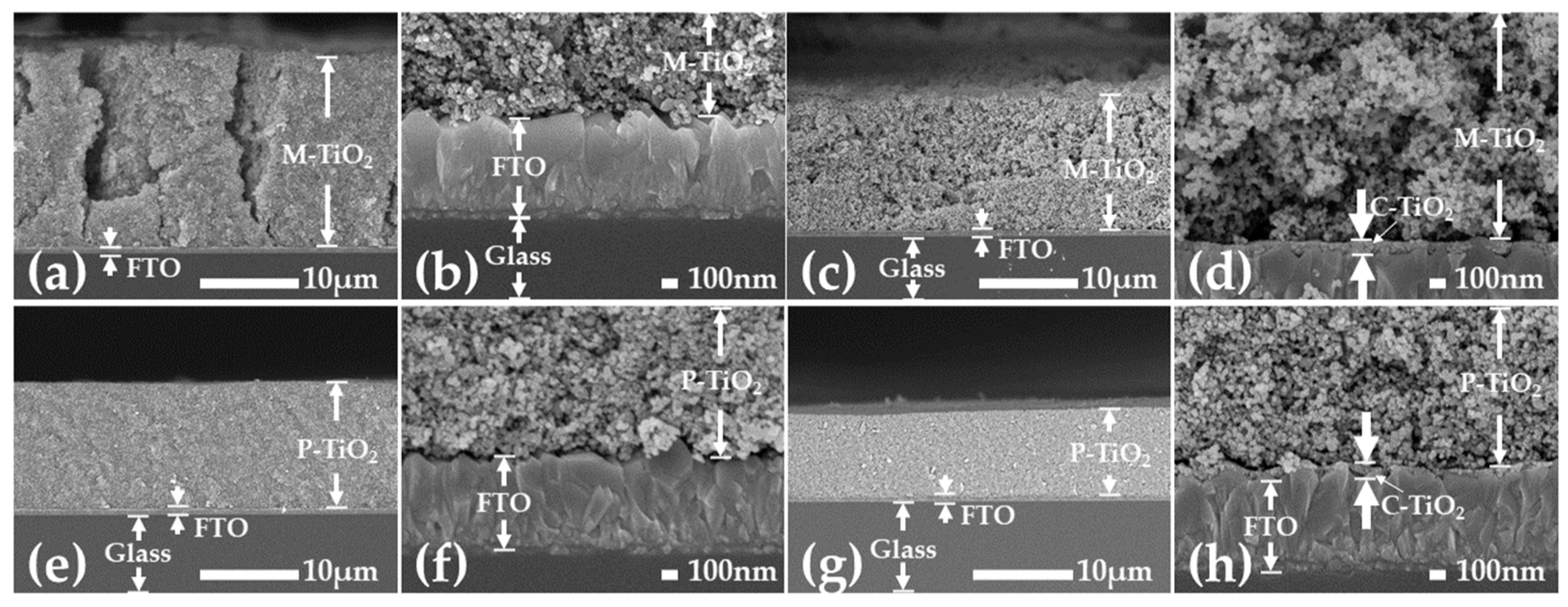
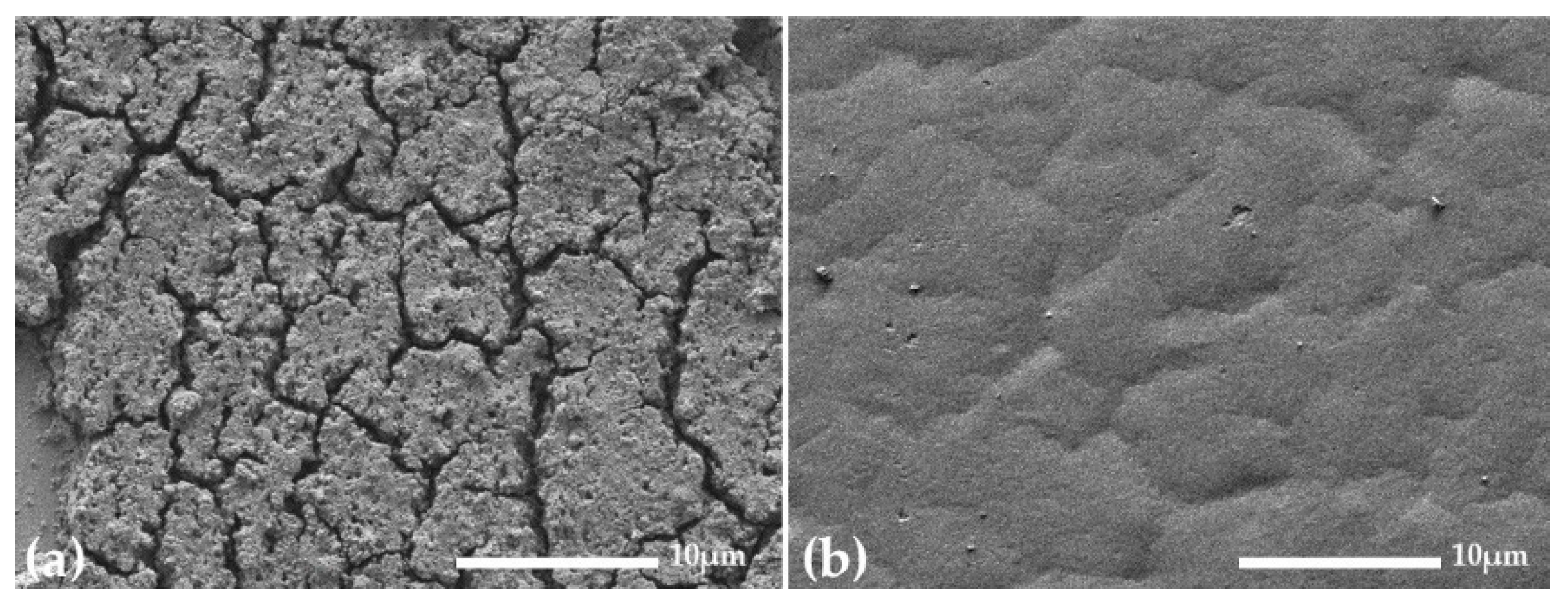
2.3.1. Preparation of Mesoporous TiO2 NPs Layer
2.3.2. Preparation of Compact TiO2 Thin Film
2.3.3. Preparation of Pressed TiO2 NPs Layer
2.4. DSSC Fabrication
2.5. Characterization
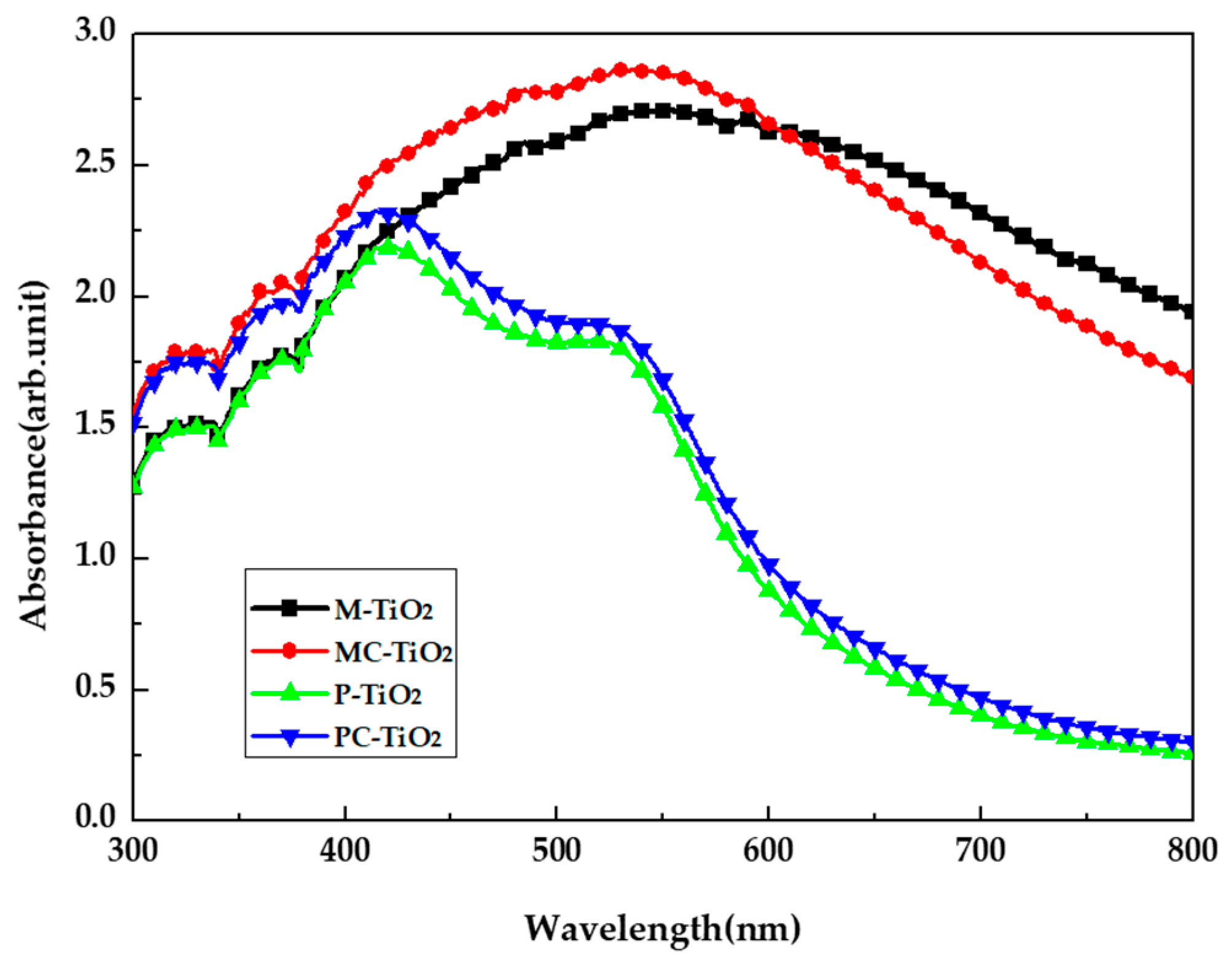
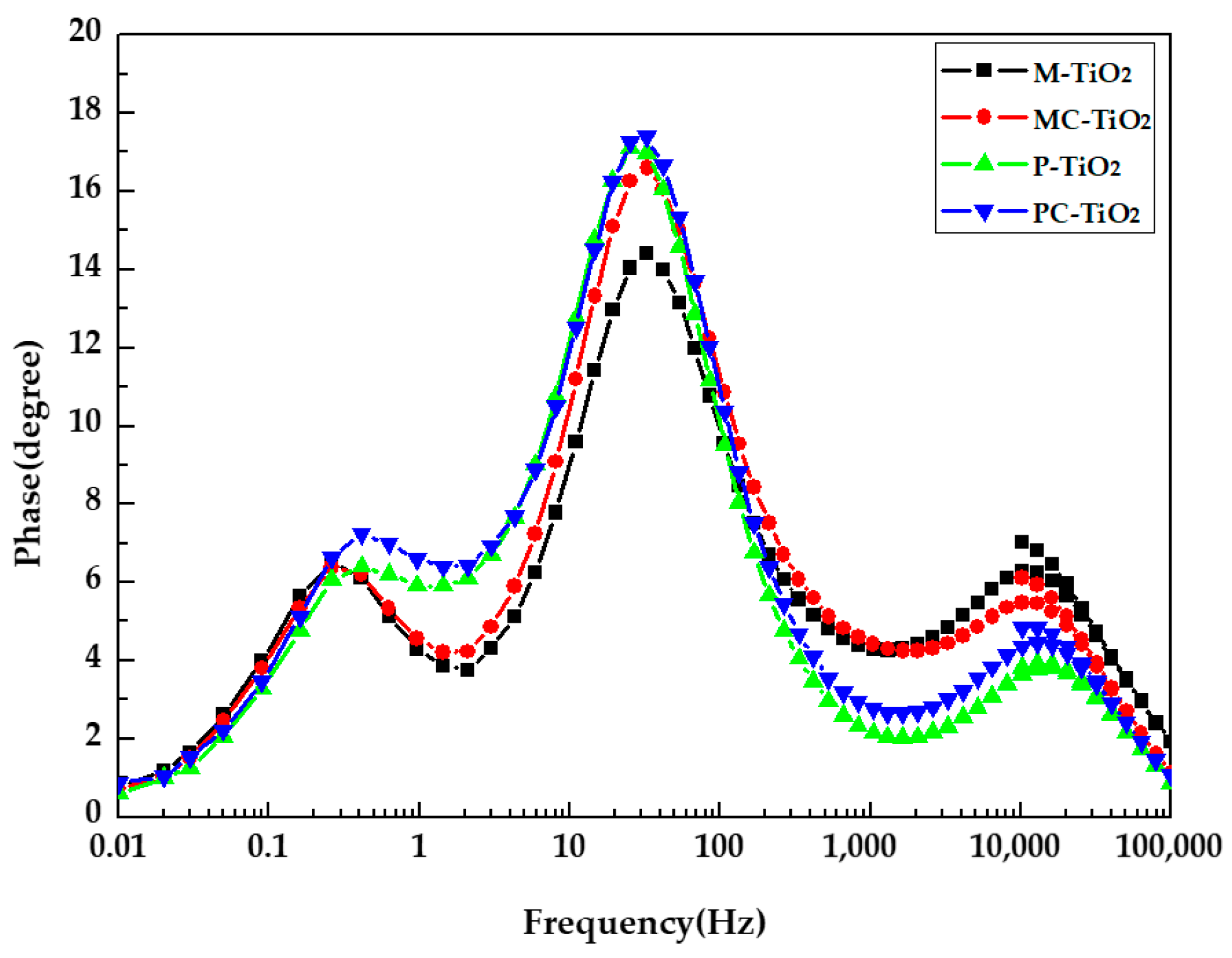
3. Results
4. Conclusions
Author Contributions
Funding
Institutional Review Board Statement
Informed Consent Statement
Data Availability Statement
Conflicts of Interest
References
- Lewis, N.S.; Crabtree, G.; Nozik, A.J.; Wasielewski, M.R.; Alivisatos, P.; Kung, H.; Spitler, M. Basic Research Needs for Solar Energy Utilization. Report of the Basic Energy Sciences Workshop on Solar Energy Utilization, 18–21 April 2005; USDOE Office of Science (SC): Washington, D.C., USA, 2005. [CrossRef]
- Rathore, N.; Panwar, N.L.; Yettou, F.; Gama, A. A comprehensive review of different types of solar photovoltaic cells and their applications. Int. J. Ambient. Energy 2021, 42, 1200–1217. [Google Scholar] [CrossRef]
- Gong, J.; Sumathy, K.; Qiao, Q.; Zhou, Z. Review on dye sensitized solar cells (DSSCs): Advanced techniques and research trends. Renew. Sustain. Energy Rev. 2017, 68, 234–246. [Google Scholar] [CrossRef]
- Karim, N.A.; Mehmood, U.; Zahid, H.F.; Asif, T. Nanostructured photoanode and counter electrode materials for efficient Dye-Sensitized Solar Cells (DSSCs). Sol. Energy 2019, 185, 165–188. [Google Scholar] [CrossRef]
- Mustafa, M.N.; Sulaiman, Y. Review on the effect of compact layers and light scattering layers on the enhancement of dye sensitized solar cells. Sol. Energy 2021, 215, 26–43. [Google Scholar] [CrossRef]
- Kim, M.H.; Kwon, Y.U. Semiconductor CdO as a Blocking Layer Material on DSSC Electrode: Mechanism and Application. J. Phys. Chem. C 2009, 113, 17176–17182. [Google Scholar] [CrossRef]
- Krumpmann, A.; Dervaux, J.; Derue, L.; Douhéret, O.; Lazzaroni, R.; Snyders, R.; Decroly, A. Influence of a sputtered compact TiO2 layer on the properties of TiO2 nanotube photoanodes for solid state DSSCs. Mater. Des. 2017, 120, 298–306. [Google Scholar] [CrossRef]
- Wang, J.; Wang, J.; Ding, J.; Wei, Y.; Zhang, J. Preparation of ZnO compact layer using vacuum ultraviolet for dye sensitized solar cells. Solid State Sci. 2022, 127, 106860. [Google Scholar] [CrossRef]
- Gnida, P.; Slodek, A.; Chulkin, P.; Vasylieva, M.; Pająk, A.K.; Seweryn ASchab Balcerzak, E. Schab-Balcerzak E. Impact of blocking layer on DSSC performance based on new dye-indolo [3, 2, 1-jk] carbazole derivative and N719. Dye. Pigment. 2022, 200, 110166. [Google Scholar] [CrossRef]
- Chang, H.; Chen, C.H.; Kao, M.J.; Chien, S.H.; Chou, C.Y. Photoelectrode thin film of dye sensitized solar cell fabricated by anodizing method and spin coating and electrochemical impedance properties of DSSC. Appl. Surf. Sci. 2013, 275, 252–257. [Google Scholar] [CrossRef]
- Nisticò, R.; Scalarone, D.; Magnacca, G. Sol gel chemistry, templating and spin coating deposition: A combined approach to control in a simple way the porosity of inorganic thin films/coatings. Microporous Mesoporous Mater. 2017, 248, 18–29. [Google Scholar] [CrossRef]
- Niu, H.; Xie, Y.; Shao, J.; Ye, T.; Li, T.W. Synergy light trapping enhanced solar energy conversion in DSSCs containing texture pit and silver nanoparticles. Mater. Sci. Semicond. Process. 2022, 148, 106774. [Google Scholar] [CrossRef]
- Ahmed AS, A.; Xiang, W.; Hashem FS, M.; Zhao, X. Screen printed carbon black/SiO2 composite counter electrodes for dye sensitized solar cells. Sol. Energy 2021, 230, 902–911. [Google Scholar] [CrossRef]
- Rubino, A.; Queirós, R. Electrochemical determination of heavy metal ions applying screen printed electrodes based sensors. A review on water and environmental samples analysis. Talanta Open 2023, 7, 100203. [Google Scholar] [CrossRef]
- Tsai, J.K.; Hsu, W.D.; Wu, T.C.; Meen, T.H.; Chong, W.J. Effect of compressed TiO2 nanoparticle thin film thickness on the performance of dye sensitized solar cells. Nanoscale Res. Lett. 2013, 8, 459. [Google Scholar] [CrossRef] [PubMed]
- Meen, T.H.; Tsai, J.K.; Tu, Y.S.; Wu, T.C.; Hsu, W.D.; Chang, S.J. Optimization of the dye sensitized solar cell performance by mechanical compression. Nanoscale Res. Lett. 2014, 9, 523. [Google Scholar] [CrossRef] [PubMed]
- Huang, W.M.; Tsai, J.K.; Wu, T.C.; Meen, T.H. Improvement of Dye sensitized Solar Cells by Using Compact and Pressed Layer of TiO2. In Proceedings of the 2022 IEEE 5th International Conference on Knowledge Innovation and Invention (ICKII ), Yunlin, Taiwan, 22–24 July 2022. [Google Scholar]
- Oku, T.; Ohishi, Y.; Suzuki, A.; Miyazawa, Y. Effects of NH4Cl addition to perovskite CH3NH3PbI3 photovoltaic devices. J. Ceram. Soc. Jpn. 2017, 125, 303–307. [Google Scholar] [CrossRef]
- Taleb, A.; Mesguish, F.; Yanpeng, X. Effect of cracking and aggregation on the efficiency of DSSC. In Proceedings of the International Renewable and Sustainable Energy Conference (IRSEC), Ouazazate, Morocco, 17–19 October 2014. [Google Scholar]
- Chang, H.; Su, H.T.; Chen, W.A.; David Huang, K.; Chien, S.H.; Chen, S.L.; Chen, C.C. Fabrication of multilayer TiO2 thin films for dye sensitized solar cells with high conversion efficiency by electrophoresis deposition. Sol. Energy 2010, 84, 130–136. [Google Scholar] [CrossRef]
- Jang, S.R.; Vittal, R.; Lee, J.; Jeong, N.; Kim, K.J. Linkage of N3 dye to N3 dye on nanocrystalline TiO2 through trans 1,2 bis(4 pyridyl)ethylene for enhancement of photocurrent of dye sensitized solar cells. Chem. Commun. 2006, 1, 103–105. [Google Scholar] [CrossRef] [PubMed]
- Zhao, X.G.; Park, J.Y.; Jin, E.M.; Gu, H.B. Tuning the Interfacial Area and Porosity of TiO2 Film for Enhanced Light Harvesting in DSSC. J. Electrochem. Soc. 2015, 162, E1. [Google Scholar] [CrossRef]
- Huang, J.J.; Ou, S.L.; Hsu, C.F.; Shen, X.Q. The effect of boric acid concentration on the TiO2 compact layer by liquid phase deposition for dye sensitized solar cell. Appl. Surf. Sci. 2019, 477, 7–14. [Google Scholar] [CrossRef]
- Huang, J.S. Dynamics of Metal Free Organic Dyes under Various Conditions and Their Applications in Dye Sensitized Solar Cells; M. S. Program, Department of Applied Chemistry, National Chiao Tung University: Hsinchu, Taiwan, 2011. [Google Scholar] [CrossRef]


| TiO2 Layer | RS (Ω) | RPT (Ω) | RK (Ω) | RD (Ω) | (s−1) | τeff (ms) |
|---|---|---|---|---|---|---|
| Mesoporous TiO2 NPs layer | 14.78 | 3.78 | 12.94 | 5.26 | 25.32 | 6.287 |
| Mesoporous TiO2 NPs layer on compact TiO2 thin film | 13.04 | 2.54 | 13.57 | 4.28 | 25.32 | 6.287 |
| Pressed TiO2 NPs layer | 13.74 | 2.00 | 14.66 | 6.75 | 19.37 | 8.217 |
| Pressed TiO2 NPs layer on compact TiO2 thin film | 12.89 | 2.20 | 13.53 | 6.20 | 19.37 | 8.217 |
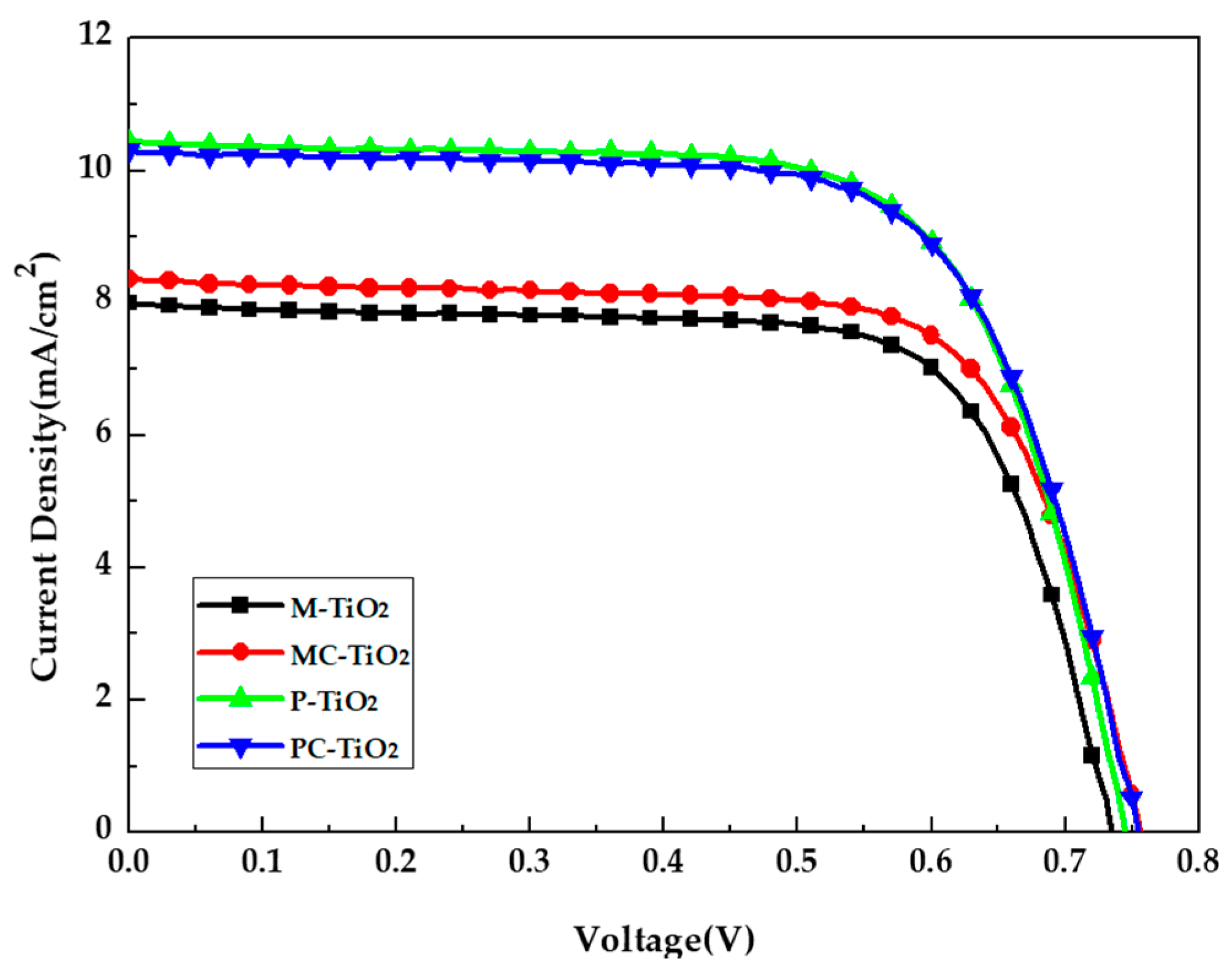
| TiO2 Layer | VOC (V) | JSC (mA/cm2) | F.F. (%) | PCE (%) |
|---|---|---|---|---|
| Mesoporous TiO2 NPs layer | 0.74 | 7.66 | 71.66 | 4.08 |
| Mesoporous TiO2 NPs layer on compact TiO2 thin film | 0.76 | 8.36 | 71.31 | 4.51 |
| Pressed TiO2 NPs layer | 0.74 | 10.43 | 69.54 | 5.40 |
| Pressed TiO2 NPs layer on compact TiO2 thin film | 0.75 | 10.30 | 69.01 | 5.36 |
Disclaimer/Publisher’s Note: The statements, opinions and data contained in all publications are solely those of the individual author(s) and contributor(s) and not of MDPI and/or the editor(s). MDPI and/or the editor(s) disclaim responsibility for any injury to people or property resulting from any ideas, methods, instructions or products referred to in the content. |
© 2023 by the authors. Licensee MDPI, Basel, Switzerland. This article is an open access article distributed under the terms and conditions of the Creative Commons Attribution (CC BY) license (https://creativecommons.org/licenses/by/4.0/).
Share and Cite
Wu, T.-C.; Huang, W.-M.; Meen, T.-H.; Tsai, J.-K. Performance Improvement of Dye-Sensitized Solar Cells with Pressed TiO2 Nanoparticles Layer. Coatings 2023, 13, 907. https://doi.org/10.3390/coatings13050907
Wu T-C, Huang W-M, Meen T-H, Tsai J-K. Performance Improvement of Dye-Sensitized Solar Cells with Pressed TiO2 Nanoparticles Layer. Coatings. 2023; 13(5):907. https://doi.org/10.3390/coatings13050907
Chicago/Turabian StyleWu, Tian-Chiuan, Wei-Ming Huang, Teen-Hang Meen, and Jenn-Kai Tsai. 2023. "Performance Improvement of Dye-Sensitized Solar Cells with Pressed TiO2 Nanoparticles Layer" Coatings 13, no. 5: 907. https://doi.org/10.3390/coatings13050907