Communication

Adsorption and Surface Diffusion of Atomic Ru on TiN and SiO2: A First-Principles Study

Department of Chemical Engineering, Hongik University, Seoul 04066, Republic of Korea
*
Authors to whom correspondence should be addressed.
Coatings 2023, 13(6), 1020; https://doi.org/10.3390/coatings13061020
Submission received: 9 May 2023 / Revised: 26 May 2023 / Accepted: 29 May 2023 / Published: 31 May 2023
(This article belongs to the Special Issue Advanced Films and Coatings Based on Atomic Layer Deposition)

Abstract

:
Ruthenium (Ru) has been suggested as one of the promising materials for nanoscale interconnects to substitute copper (Cu) that is currently used in the semiconductor industry. Through density functional theory (DFT) calculations, we present the rationales for varying deposition behavior of Ru on different types of substrates. For the SiO2 and TiN substrates, with and without adsorbed hydrogen, our calculation results reveal the adsorption sites and their adsorption energy, the surface diffusion paths and their activation energy, and the surface diffusion coefficients. We confirm that the adsorption of Ru is more stable on TiN than on SiO2 substrates, and that the surface diffusion of Ru adatom is faster on TiN than on SiO2 surface.

1. Introduction

Electronic devices have evolved into highly integrated low-power driving devices due to scaling down. Transistors have been continuously developed from a two-dimensional planar structure to three-dimensional structures such as FinFET and GAA (gate all around), whose minimal pitch size is approaching the thickness of tens of atoms. Accordingly, metal interconnects within such nanoscale electronic devices must also be fabricated at nm scale. The interconnect materials for the future semiconductor devices also have to satisfy the characteristics of thermal stability, good adhesion to substrates, low resistivity, high reliability, and ease of pattern formation [1,2]. By virtue of its low resistivity, copper (Cu) has been the widespread material for metallization of interconnects in semiconductor devices. However, diffusion of Cu through insulation layers can occur, requiring additional diffusion barrier layers such as TiN or TaN [3]. While the feature width of the interconnects has been scaled down in recent devices, the thickness of the diffusion barrier could not be reduced in accordance. In addition, as the width of the interconnects decreases, the current density within the interconnects increases, causing electromigration and a rapid increase in specific resistance. Furthermore, the electron mean free path of bulk Cu is large, such that when Cu is used with a linewidth of several nm, its specific resistance rapidly increases according to grain boundary scattering. Accordingly, research on various alternative interconnect materials whose specific resistance is less increased even at nanoscale linewidths is actively being conducted. Among them, ruthenium (Ru) may be a promising material due to its relatively shorter electron mean free path [4,5,6]. In addition, Ru may not require a diffusion barrier layer like Cu. Therefore, together with its higher melting point than Cu, Ru is considered an alternative nanoscale interconnect material.
On the other hand, achieving a high-aspect-ratio structure in the semiconductor fabrication process is highly challenging. To overcome such difficulty, the area-selective deposition (ASD) technique is being developed, which allows deposition to take place only on a specific, desired surface according to the difference in chemistry of the substrate surface via chemical vapor deposition (CVD) or atomic layer deposition (ALD) [7,8]. When it comes to the deposition of Ru, selectivity between SiO2 and TiN substrates is often desirable, as the former is an interlayer dielectric (ILD) material preventing the metal wiring from interference, while the latter is deposited as a diffusion barrier for the metal into the ILD. Previous experimental studies have often shown that deposition of Ru exhibited more significant nucleation delay or island-type growth on SiO2 substrates, whereas less nucleation delay and fast nucleation were achieved on TiN substrates [9,10,11,12,13,14]. While there is continuing debate on the underlying mechanisms that govern the deposition selectivity of Ru on different substrates, such as the adsorption chemistry of the precursors, differences in electronegativity, and differences in the interfacial energy, the relative rate of surface diffusion has been recently suggested to play a role [15,16,17,18]. Since strong dependence on the substrate materials is often observed during the initial nucleation of Ru thin films for either physical deposition methods such as sputtering and chemical deposition methods such as CVD or ALD [19,20,21], it can be suspected that surface-dependent adsorption is a significant fundamental property of Ru.
Surface and interface diffusion is crucial in a variety of applications including thin-film growth, fabrication of microelectronic devices, and material corrosion processes [22]. The rate of surface diffusion tends to be highly dependent on the temperature as enough thermal energy needs to be supplied to the diffusing atoms to overcome the activation energy barriers. The activation energy of surface diffusion, which needs to be overcome when the metal atoms diffuse from one adsorption site to another, can be modified when the type or condition of the substrate surface differs. Therefore, the surface diffusion rate, as well as its behavior, obviously depends on the substrate materials and their surface preparation conditions [23]. Atomistic simulations based on first-principles calculations are often shown to be powerful in estimating the diffusion coefficients [24,25], as recent studies on technologically important surfaces such as TiN and SiO2 have shown [26,27,28,29,30,31,32,33,34,35,36,37].
In this study, we explored the adsorption and surface diffusion of atomic Ru on surfaces of TiN and SiO2. With different substrate conditions regarding hydrogenation, we analyzed the difference in the adsorption and surface diffusion mechanisms using density functional theory (DFT). Our results quantitatively confirmed the deposition characteristics on each different substrates, indicating that deposition of Ru on TiN would be preferred over that on SiO2.

2. Methods

Vienna ab initio simulation package (VASP) version 5.4.4 [38] was used for DFT calculations. The Perdew–Burke–Ernzerhof (PBE) functional [39] based on generalized gradient approximation (GGA) was used to calculate the electron density, together with the D3 method, applying Becke–Johnson damping for dispersion correction [40]. From benchmark studies in the literature, it is known that the performance of the PBE-D3 method toward the estimation of surface adsorption energies is comparable to other functionals [41,42]. To model the substrates, the most stable bulk structures of α-quartz SiO2 (001) [43] and cubic TiN (100) [44] were obtained [45]. SiO2 with full coverage of hydroxyls (OH) and TiN with 50% H coverage, where the hydrogen adatoms are present on top of the nitrogen sites, were additionally created. A vacuum of 15 Å was formed on the z-axis to optimize the slab structure. The SiO2 substrate was optimized with a cutoff energy of 400 eV and Monkhorst-Pack k-point mesh of 3 × 3 × 1, while the TiN substrate was optimized with a cutoff energy of 450 eV and Monkhorst-Pack k-point mesh 5 × 5 × 1. The adsorption energy ΔEads, designated to the adsorption site for ruthenium atoms, was calculated using the following equation:
E a d s = E m o l e . a d s E s l a b + E R u ,
where Emole.ads is the ground-state energy in the state where a ruthenium atom is adsorbed on the slab surface, and Eslab and ERu represent the energy of each slab and ruthenium atom, respectively. The transition states for the diffusion process were analyzed using the climbing image nudged elastic band (CI-NEB) method [46] to evaluate the diffusion barrier along the surface diffusion path of ruthenium atoms. The following relational expression was used for calculating the activation energy (Ea) for the surface diffusion:
E a = E t r a n s E m o l e . a d s ,
where Etrans is the transition state energy obtained from the CI-NEB calculation. The surface diffusion coefficient D can be calculated using the following equation [47]:
D = ν a 2 4 e E a / k b T ,
where ν is the jump frequency (assumed to be 1013 s−1), a is the step distance (assumed to be 0.3 nm), kb is the Boltzmann constant, and T is the deposition temperature.

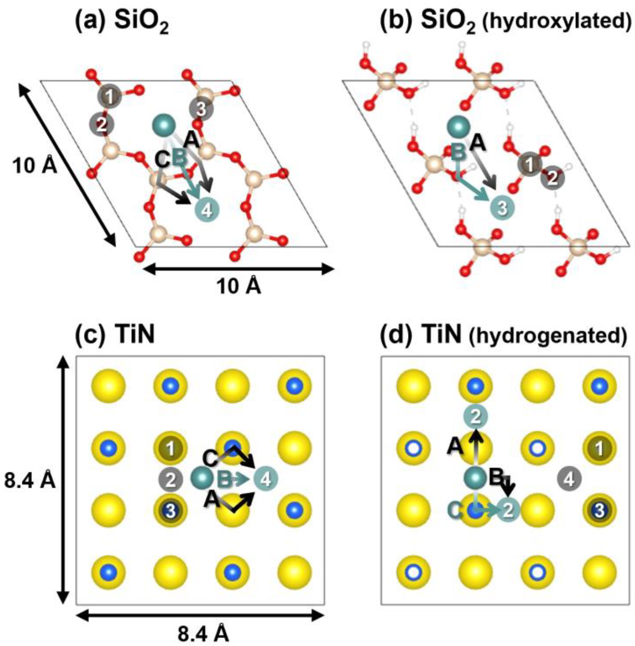
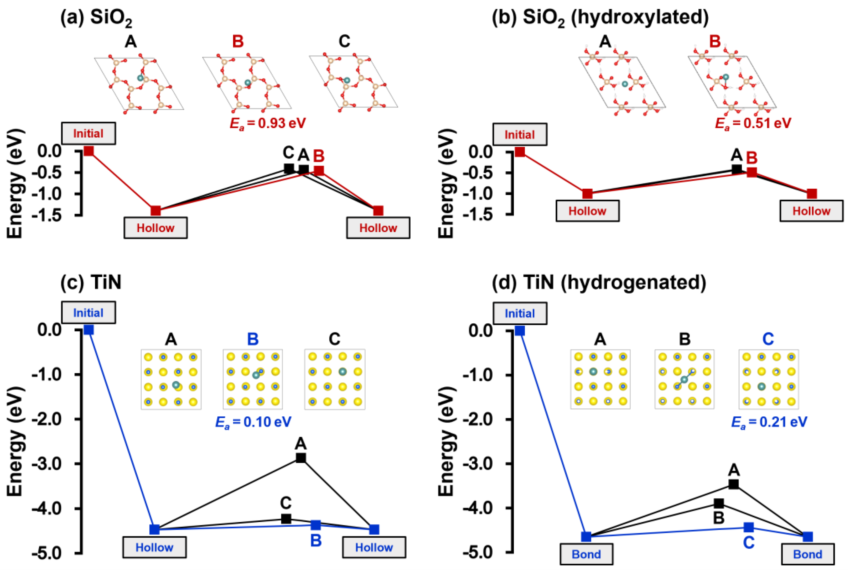
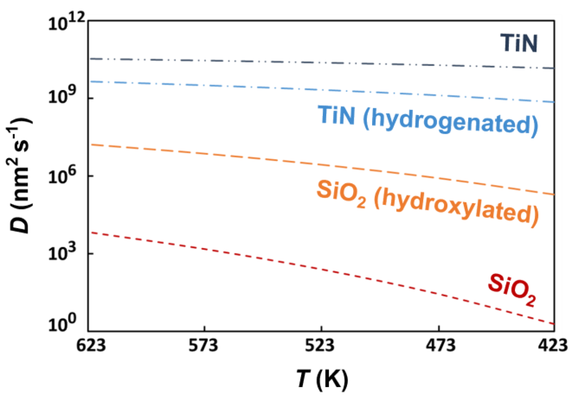
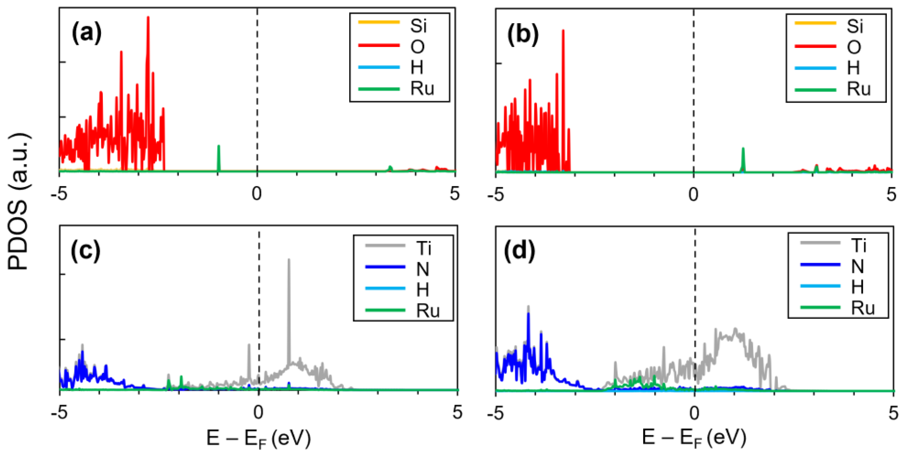
3. Results and Discussion

Labeled with digits in Figure 1, the possible adsorption sites for Ru atoms are presented for the SiO2 and TiN substrates. For the SiO2 substrate, four different adsorption sites are identified: Si atom, O atom, Si–O bond, and hollow; the adsorption site at the Si–O bond is excluded for the hydroxylated SiO2 substrate, since such a structure could not be properly optimized. Similarly, the TiN substrate, with or without hydrogen doping, provides four adsorption sites for ruthenium atoms: N atom, Ti–N bond, Ti atom, and hollow.
To find the most stable adsorption site for Ru adatoms, the adsorption energy ΔEads was calculated and compared for the different sites on each substrate (Table 1). The hollow site was confirmed as the most stable adsorption site for both pristine and hydroxylated SiO2 substrates. The results also indicate that the other sites in the SiO2 substrates were relatively unstable. While the pristine TiN substrate provided the lowest adsorption energy at the hollow site similarly to the SiO2 cases, the hydrogenated TiN presented the most stable adsorption site at the Ti–N bond. This implies that the hydrogen doping may present an impact on the change in local atomic and electronic structures of substrate materials, which leads to the difference in the adsorption chemistry of ruthenium atoms. In addition, the TiN substrates exhibit about fourfold higher adsorption energy of ca. 4.5 eV than those on the SiO2 substrates of ca. 1.2 eV. Such results suggest that the TiN substrates would show better adhesion characteristics for the Ru thin films [48], as well as preferential adsorption and deposition than the SiO2 substrates, which corroborates previous experimental results.
On the basis of the analysis regarding the adsorption sites, the available paths of a Ru adatom for the surface diffusion are examined for each substrate as shown in Figure 1 (labelled with letters). The surface diffusion paths are assumed such that a Ru adatom on the most stable adsorption site diffuses to the closest identical adsorption site.
In Figure 2, the most favorable path is confirmed by calculating the activation energy Ea for the surface diffusion of a Ru atom. For both pristine and hydroxylated SiO2 substrates, the lowest activation energy is achieved when the ruthenium atom diffuses over an oxygen atom. The pristine TiN substrate shows the minimal diffusion barrier for the diffusion across a Ti–N bond, while the hydrogenated TiN presents it for the diffusion over a nitrogen atom. By decreasing the activation energy, the hydrogen doping quantitatively changes the diffusion barrier of the ruthenium atoms on the SiO2 substrates. Hydrogen-adsorbed TiN, on the other hand, shows smaller Ea for Ru diffusion compared to bare TiN, although the difference according to presence of H is only in the order of 0.1 eV. Overall, the Ea values for surface diffusion of Ru along the most favorable paths are significantly smaller on TiN substrates (0.1–0.2 eV) compared to SiO2 substrates (0.5–0.9 eV).
Figure 3 presents the calculated surface diffusion coefficients of Ru adatoms for each substrate over a range of temperature. The highest surface diffusion coefficient is achieved on the pristine TiN substrate, whereas the pristine SiO2 substrate provides the lowest one, which is consistent with our discussion above, as well as the aforementioned experimental results. If both TiN and SiO2 surfaces are covered by hydrogen adatoms, the surface diffusion coefficient of Ru is at least 200-fold larger on TiN than on SiO2; if both surfaces are bare without H adatoms, the surface diffusion coefficient on TiN can be more than 5 × 10⁶-fold greater than that on the SiO2 surface. The relative difference in the surface diffusion coefficients between SiO2 and TiN substrates is large enough over typical temperature ranges for Ru ALD of around 450–650 K [49], such that the area-selective deposition of Ru may be accomplished by means of surface diffusion on substrates patterned with SiO2/TiN.
The analysis on the adsorption sites and their adsorption energy, the surface diffusion paths and their activation energy, and the surface diffusion coefficient enables us to suggest the rationales for different deposition natures of Ru on the SiO2 and TiN substrates. The low surface diffusion coefficient of Ru for the SiO2 substrates, which is derived from the high activation energy for the surface diffusion, can explain the island growth of Ru on them, while the opposite results are used to clarify how the layer-by-layer deposition is achieved on the TiN substrates.
In order to explore the electronic structures of the Ru-adsorbed substrates, the projected density of state (PDOS) of the most stable adsorption configurations of Ru on each surface is obtained, as summarized in Figure 4. While SiO2 substrates are insulating with significant bandgaps (Figure 4a,b), the TiN surfaces indicate a metallic nature without a measurable bandgap (Figure 4c,d). It is found that the position of Ru orbitals on SiO2 is dependent on the presence of H atoms on the surface, although the most stable adsorption site for Ru was determined for both bare and hydroxylated SiO2 surfaces. On bare SiO2, a sharp peak of the Ru 4d state is observed under EF (Fermi level) of ca. −0.97 eV, while, on hydroxylated SiO2, Ru 4d peaks at 1.25 eV above EF. On the other hand, in the case of TiN, the Ru states are distributed over the range of ca. −2.5 to −1 eV under EF, regardless of hydrogenation. Thus, there exists a fundamental difference in the chemical mechanism for adsorption of Ru adatom on SiO2 and TiN surfaces, which may deserve future research attention.

4. Conclusions

In this study, we analyzed the adsorption and diffusion behavior of ruthenium atoms on SiO2 and TiN surfaces. DFT calculations were performed for the adsorption site-dependent adsorption energy, the activation energy dependent to surface diffusion paths, and the surface diffusion coefficient. We confirmed that the adsorption of Ru atoms is significantly more stable on the TiN substrates than the SiO2 substrates regardless of pre-existing hydrogen, such that the adsorption energy of Ru on TiN is ca. fourfold larger than on SiO2. Moreover, the surface diffusion of Ru on TiN is several orders faster than on SiO2 surfaces. Our analysis can be used to explain the reported experimental results that the SiO2 substrates often show island growth during Ru deposition, while the TiN substrates exhibit layer-by-layer deposition of Ru, as well as the finding that adhesion of Ru is stronger on TiN than on SiO2.

Author Contributions

Conceptualization, B.S.; Methodology, C.A. and J.H.J.; Software, C.A.; Validation, C.A. and J.H.J.; Formal analysis, C.A., J.H.J., J.J.K. and D.-C.L.; Investigation, C.A. and J.H.J.; Resources, C.A., J.H.J. and B.S.; Data curation, C.A., J.H.J. and B.S.; Writing—original draft, C.A. and J.H.J.; Writing—review & editing, J.J.K., D.-C.L. and B.S.; Visualization, C.A., J.H.J. and D.-C.L.; Supervision, B.S.; Project administration, B.S.; Funding acquisition, B.S. All authors have read and agreed to the published version of the manuscript.

Funding

This research was supported by the MOTIE (Ministry of Trade, Industry, and Energy, RS-2023-00236667) and KSRC (Korea Semiconductor Research Consortium, 20024793) support program for the development of the future semiconductor device, by a Korea Institute for Advancement of Technology (KIAT) grant funded by the Korea Government (MOTIE; P0012451, The Competency Development Program for Industry Specialist), and by the National Research Foundation of Korea (NRF) funded by the Korean Government (MSIT, RS-2023-00210186).

Institutional Review Board Statement

Not applicable.

Informed Consent Statement

Not applicable.

Data Availability Statement

Not applicable.

Conflicts of Interest

The authors declare no conflict of interest.

References

  1. Lee, M.H.; Shue, W.S. The Overview of Current Interconnect Technology Challenges and Future Opportunities. In Proceedings of the 2020 IEEE International Electron Devices Meeting (IEDM), San Francisco, CA, USA, 12–18 December 2020; pp. 32.1.1–32.1.4. [Google Scholar]
  2. Baklanov, M.R.; Adelmann, C.; Zhao, L.; Gendt, S.D. Advanced Interconnects: Materials, Processing, and Reliability. ECS J. Solid State Sci. Technol. 2014, 4, Y1. [Google Scholar] [CrossRef]
  3. Li, Z.; Tian, Y.; Teng, C.; Cao, H. Recent Advances in Barrier Layer of Cu Interconnects. Materials 2020, 13, 5049. [Google Scholar] [CrossRef]
  4. Adelmann, C.; Sankaran, K.; Dutta, S.; Gupta, A.; Kundu, S.; Jamieson, G.; Moors, K.; Pinna, N.; Ciofi, I.; Van Eishocht, S.; et al. Alternative Metals: From Ab Initio Screening to Calibrated Narrow Line Models. In Proceedings of the 2018 IEEE International Interconnect Technology Conference (IITC), Santa Clara, CA, USA, 4–7 June 2018; pp. 154–156. [Google Scholar]
  5. Gall, D. The Search for the Most Conductive Metal for Narrow Interconnect Lines. J. Appl. Phys. 2020, 127, 050901. [Google Scholar] [CrossRef]
  6. Dutta, S.; Moors, K.; Vandemaele, M.; Adelmann, C. Finite Size Effects in Highly Scaled Ruthenium Interconnects. IEEE Electron Device Lett. 2018, 39, 268–271. [Google Scholar] [CrossRef]
  7. Mackus, A.J.M.; Merkx, M.J.M.; Kessels, W.M.M. From the Bottom-Up: Toward Area-Selective Atomic Layer Deposition with High Selectivity. Chem. Mater. 2019, 31, 2–12. [Google Scholar] [CrossRef]
  8. Parsons, G.N.; Clark, R.D. Area-Selective Deposition: Fundamentals, Applications, and Future Outlook. Chem. Mater. 2020, 32, 4920–4953. [Google Scholar] [CrossRef]
  9. Kim, S.K.; Han, J.H.; Kim, G.H.; Hwang, C.S. Investigation on the Growth Initiation of Ru Thin Films by Atomic Layer Deposition. Chem. Mater. 2010, 22, 2850–2856. [Google Scholar] [CrossRef]
  10. Han, J.H.; Lee, S.W.; Kim, S.K.; Han, S.; Lee, W.; Hwang, C.S.; Dussarat, C.; Gatineau, J. Study on Initial Growth Behavior of RuO2 Film Grown by Pulsed Chemical Vapor Deposition: Effects of Substrate and Reactant Feeding Time. Chem. Mater. 2012, 24, 1407–1414. [Google Scholar] [CrossRef]
  11. Jung, H.J.; Han, J.H.; Jung, E.A.; Park, B.K.; Hwang, J.-H.; Son, S.U.; Kim, C.G.; Chung, T.-M.; An, K.-S. Atomic Layer Deposition of Ruthenium and Ruthenium Oxide Thin Films from a Zero-Valent (1,5-Hexadiene)(1-Isopropyl-4-Methylbenzene)Ruthenium Complex and O2. Chem. Mater. 2014, 26, 7083–7090. [Google Scholar] [CrossRef]
  12. Popovici, M.; Groven, B.; Marcoen, K.; Phung, Q.M.; Dutta, S.; Swerts, J.; Meersschaut, J.; van den Berg, J.A.; Franquet, A.; Moussa, A.; et al. Atomic Layer Deposition of Ruthenium Thin Films from (Ethylbenzyl) (1-Ethyl-1,4-Cyclohexadienyl) Ru: Process Characteristics, Surface Chemistry, and Film Properties. Chem. Mater. 2017, 29, 4654–4666. [Google Scholar] [CrossRef]
  13. Hwang, J.M.; Han, S.-M.; Yang, H.; Yeo, S.; Lee, S.-H.; Park, C.W.; Kim, G.H.; Park, B.K.; Byun, Y.; Eom, T.; et al. Atomic Layer Deposition of a Ruthenium Thin Film Using a Precursor with Enhanced Reactivity. J. Mater. Chem. C 2021, 9, 3820–3825. [Google Scholar] [CrossRef]
  14. Claessens, N.; Khan, Z.Z.; Haghighi, N.R.; Delabie, A.; Vantomme, A.; Vandervorst, W.; Meersschaut, J. Quantification of Area-Selective Deposition on Nanometer-Scale Patterns Using Rutherford Backscattering Spectrometry. Sci. Rep. 2022, 12, 17770. [Google Scholar] [CrossRef] [PubMed]
  15. Yim, S.-S.; Lee, D.-J.; Kim, K.-S.; Kim, S.-H.; Yoon, T.-S.; Kim, K.-B. Nucleation Kinetics of Ru on Silicon Oxide and Silicon Nitride Surfaces Deposited by Atomic Layer Deposition. J. Appl. Phys. 2008, 103, 113509. [Google Scholar] [CrossRef]
  16. Soethoudt, J.; Grillo, F.; Marques, E.A.; van Ommen, J.R.; Tomczak, Y.; Nyns, L.; Van Elshocht, S.; Delabie, A. Diffusion-Mediated Growth and Size-Dependent Nanoparticle Reactivity during Ruthenium Atomic Layer Deposition on Dielectric Substrates. Adv. Mater. Interfaces 2018, 5, 1800870. [Google Scholar] [CrossRef]
  17. Soethoudt, J.; Hody, H.; Spampinato, V.; Franquet, A.; Briggs, B.; Chan, B.T.; Delabie, A. Defect Mitigation in Area-Selective Atomic Layer Deposition of Ruthenium on Titanium Nitride/Dielectric Nanopatterns. Adv. Mater. Interfaces 2019, 6, 1900896. [Google Scholar] [CrossRef]
  18. Grillo, F.; Soethoudt, J.; Marques, E.A.; de Martín, L.; Van Dongen, K.; van Ommen, J.R.; Delabie, A. Area-Selective Deposition of Ruthenium by Area-Dependent Surface Diffusion. Chem. Mater. 2020, 32, 9560–9572. [Google Scholar] [CrossRef]
  19. Kang, S.Y.; Hwang, C.S.; Kim, H.J. Improvements in Growth Behavior of CVD Ru Films on Film Substrates for Memory Capacitor Integration. J. Electrochem. Soc. 2004, 152, C15. [Google Scholar] [CrossRef]
  20. Coloma Ribera, R.; van de Kruijs, R.W.E.; Sturm, J.M.; Yakshin, A.E.; Bijkerk, F. In Vacuo Growth Studies of Ru Thin Films on Si, SiN, and SiO2 by High-Sensitivity Low Energy Ion Scattering. J. Appl. Phys. 2016, 120, 065303. [Google Scholar] [CrossRef]
  21. Kim, H.-M.; Lee, J.-H.; Lee, S.-H.; Harada, R.; Shigetomi, T.; Lee, S.; Tsugawa, T.; Shong, B.; Park, J.-S. Area-Selective Atomic Layer Deposition of Ruthenium Using a Novel Ru Precursor and H2O as a Reactant. Chem. Mater. 2021, 33, 4353–4361. [Google Scholar] [CrossRef]
  22. Antczak, G.; Ehrlich, G. Surface Diffusion: Metals, Metal Atoms, and Clusters; Cambridge University Press: Cambridge, UK, 2010; ISBN 978-0-521-89983-3. [Google Scholar]
  23. Seebauer, E.G.; Allen, C.E. Estimating Surface Diffusion Coefficients. Prog. Surf. Sci. 1995, 49, 265–330. [Google Scholar] [CrossRef]
  24. Kaxiras, E. Review of Atomistic Simulations of Surface Diffusion and Growth on Semiconductors. Comput. Mater. Sci. 1996, 6, 158–172. [Google Scholar] [CrossRef]
  25. Ratsch, C.; Scheffler, M. Density-Functional Theory Calculations of Hopping Rates of Surface Diffusion. Phys. Rev. B 1998, 58, 13163–13166. [Google Scholar] [CrossRef]
  26. Tholander, C.; Alling, B.; Tasnádi, F.; Greene, J.E.; Hultman, L. Effect of Al Substitution on Ti, Al, and N Adatom Dynamics on TiN(001), (011), and (111) Surfaces. Surf. Sci. 2014, 630, 28–40. [Google Scholar] [CrossRef]
  27. Guo, F.; Wang, J.; Du, Y.; Wang, J.; Shang, S.-L.; Li, S.; Chen, L. First-Principles Study of Adsorption and Diffusion of Oxygen on Surfaces of TiN, ZrN and HfN. Appl. Surf. Sci. 2018, 452, 457–462. [Google Scholar] [CrossRef]
  28. Vakula, N.I.; Kuramshina, G.M.; Gorb, L.G.; Hill, F.; Leszczynski, J. Adsorption and Diffusion of a Silver Atom and Its Cation on α-SiO2 (001): Comparison of a Pure Surface with a Surface Containing an Al Defect. Chem. Phys. Lett. 2013, 567, 27–33. [Google Scholar] [CrossRef]
  29. Sangiovanni, D.G.; Edström, D.; Hultman, L.; Petrov, I.; Greene, J.E.; Chirita, V. Ab Initio and Classical Molecular Dynamics Simulations of N2 Desorption from TiN(001) Surfaces. Surf. Sci. 2014, 624, 25–31. [Google Scholar] [CrossRef]
  30. Sangiovanni, D.G.; Edström, D.; Hultman, L.; Petrov, I.; Greene, J.E.; Chirita, V. Ti Adatom Diffusion on TiN(001): Ab Initio and Classical Molecular Dynamics Simulations. Surf. Sci. 2014, 627, 34–41. [Google Scholar] [CrossRef]
  31. Sangiovanni, D.G.; Tasnádi, F.; Hultman, L.; Petrov, I.; Greene, J.E.; Chirita, V. N and Ti Adatom Dynamics on Stoichiometric Polar TiN(111) Surfaces. Surf. Sci. 2016, 649, 72–79. [Google Scholar] [CrossRef]
  32. Kwon, J.A.; Kim, M.-S.; Shin, D.Y.; Kim, J.Y.; Lim, D.-H. First-Principles Understanding of Durable Titanium Nitride (TiN) Electrocatalyst Supports. J. Ind. Eng. Chem. 2017, 49, 69–75. [Google Scholar] [CrossRef]
  33. Tosoni, S.; Pacchioni, G. Influence of Surface Hydroxylation on the Ru Atom Diffusion on the ZrO2(101) Surface: A DFT Study. Surf. Sci. 2017, 664, 87–94. [Google Scholar] [CrossRef]
  34. Cottom, J.; Bochkarev, A.; Olsson, E.; Patel, K.; Munde, M.; Spitaler, J.; Popov, M.N.; Bosman, M.; Shluger, A.L. Modeling of Diffusion and Incorporation of Interstitial Oxygen Ions at the TiN/SiO2 Interface. ACS Appl. Mater. Interfaces 2019, 11, 36232–36243. [Google Scholar] [CrossRef]
  35. Kondati Natarajan, S.; Nies, C.-L.; Nolan, M. Ru Passivated and Ru Doped ε-TaN Surfaces as a Combined Barrier and Liner Material for Copper Interconnects: A First Principles Study. J. Mater. Chem. C 2019, 7, 7959–7973. [Google Scholar] [CrossRef]
  36. Das, T.; Tosoni, S.; Pacchioni, G. Role of Support in Tuning the Properties of Single Atom Catalysts: Cu, Ag, Au, Ni, Pd, and Pt Adsorption on SiO2/Ru, SiO2/Pt, and SiO2/Si Ultrathin Films. J. Chem. Phys. 2021, 154, 134706. [Google Scholar] [CrossRef] [PubMed]
  37. Nies, C.-L.; Kondati Natarajan, S.; Nolan, M. Control of the Cu Morphology on Ru-Passivated and Ru-Doped TaN Surfaces—Promoting Growth of 2D Conducting Copper for CMOS Interconnects. Chem. Sci. 2022, 13, 713–725. [Google Scholar] [CrossRef]
  38. Hafner, J. Ab-Initio Simulations of Materials Using VASP: Density-Functional Theory and Beyond. J. Comput. Chem. 2008, 29, 2044–2078. [Google Scholar] [CrossRef] [PubMed]
  39. Perdew, J.P.; Burke, K.; Ernzerhof, M. Generalized Gradient Approximation Made Simple. Phys. Rev. Lett. 1996, 77, 3865–3868. [Google Scholar] [CrossRef]
  40. Grimme, S.; Ehrlich, S.; Goerigk, L. Effect of the Damping Function in Dispersion Corrected Density Functional Theory. J. Comput. Chem. 2011, 32, 1456–1465. [Google Scholar] [CrossRef]
  41. Sharada, M.S.; Karlsson, R.K.B.; Maimaiti, Y.; Voss, J.; Bligaard, T. Adsorption on Transition Metal Surfaces: Transferability and Accuracy of DFT Using the ADS41 Dataset. Phys. Rev. B 2019, 100, 035439. [Google Scholar] [CrossRef]
  42. Rehak, F.R.; Piccini, G.; Alessio, M.; Sauer, J. Including Dispersion in Density Functional Theory for Adsorption on Flat Oxide Surfaces, in Metal–Organic Frameworks and in Acidic Zeolites. Phys. Chem. Chem. Phys. 2020, 22, 7577–7585. [Google Scholar] [CrossRef]
  43. Goumans, T.P.M.; Wander, A.; Brown, W.A.; Catlow, C.R.A. Structure and Stability of the (001) α-Quartz Surface. Phys. Chem. Chem. Phys. 2007, 9, 2146–2152. [Google Scholar] [CrossRef]
  44. Marlo, M.; Milman, V. Density-Functional Study of Bulk and Surface Properties of Titanium Nitride Using Different Exchange-Correlation Functionals. Phys. Rev. B 2000, 62, 2899–2907. [Google Scholar] [CrossRef]
  45. Jung, J.H.; Oh, H.; Shong, B. Fluorination of TiN, TiO2, and SiO2 Surfaces by HF toward Selective Atomic Layer Etching (ALE). Coatings 2023, 13, 387. [Google Scholar] [CrossRef]
  46. Henkelman, G.; Uberuaga, B.P.; Jónsson, H. A Climbing Image Nudged Elastic Band Method for Finding Saddle Points and Minimum Energy Paths. J. Chem. Phys. 2000, 113, 9901–9904. [Google Scholar] [CrossRef]
  47. Gomer, R. Diffusion of Adsorbates on Metal Surfaces. Rep. Prog. Phys. 1990, 53, 917. [Google Scholar] [CrossRef]
  48. Hosseini, M.; Schaekers, M.; van der Veen, M.H.; Teugels, L.; Batuk, D.; Martinez, G.T.; Yu, H.; Jourdan, N.; Schleicher, F.; Debruyn, H.; et al. Ru as an Alternative Material for Advanced Contacts. In Proceedings of the 2020 IEEE International Interconnect Technology Conference (IITC), San Jose, CA, USA, 5–8 October 2020; pp. 157–159. [Google Scholar]
  49. Kotsugi, Y.; Han, S.-M.; Kim, Y.-H.; Cheon, T.; Nandi, D.K.; Ramesh, R.; Yu, N.-K.; Son, K.; Tsugawa, T.; Ohtake, S.; et al. Atomic Layer Deposition of Ru for Replacing Cu-Interconnects. Chem. Mater. 2021, 33, 5639–5651. [Google Scholar] [CrossRef]
Figure 1. Available adsorption sites (labeled with digits, as defined in Table 1) and surface diffusion paths (labeled with letters) of ruthenium atoms on different substrates: (a) SiO2; (b) hydroxylated SiO2; (c) TiN; (d) hydrogenated TiN. The most stable adsorption sites and the most favorable surface diffusion paths are highlighted in turquoise. Ru = green, Si = tan, O = red, H = white, Ti = yellow, N = blue.
Coatings 13 01020 g001
Figure 2. Diffusion energy diagrams of Ru atoms for each substrate: (a) SiO2; (b) hydroxylated SiO2; (c) TiN; (d) hydrogenated TiN. The most favorable surface diffusion path with its activation energy is highlighted in color for each substrate.
Coatings 13 01020 g002
Figure 3. Calculated surface diffusion coefficients of Ru atoms for each substrate.
Coatings 13 01020 g003
Figure 4. Projected density of states (PDOS) plots of the Ru adsorption structures on different substrates: (a) SiO2 (hollow); (b) hydroxylated SiO2 (hollow); (c) TiN (hollow); (d) hydrogenated TiN (Ti–N bond).
Coatings 13 01020 g004
Table 1. Adsorption energy of Ru atom on each adsorption site as shown on Figure 1.
SubstrateAdsorption SiteAdsorption Energy (eV)
(a) SiO2① Si atom−0.61
② O atom−0.62
③ Si-O bond−0.61
④ Hollow−1.39
(b) SiO2 (hydroxylated)① Si atom−0.53
② O atom−0.43
③ Hollow−1.00
(c) TiN① Ti atom−2.98
② Ti–N bond−4.24
③ N atom−4.39
④ Hollow−4.47
(d) TiN (hydrogenated)① Ti atom−3.47
② Ti–N bond−4.65
③ N atom−4.45
④ Hollow −3.91
Disclaimer/Publisher’s Note: The statements, opinions and data contained in all publications are solely those of the individual author(s) and contributor(s) and not of MDPI and/or the editor(s). MDPI and/or the editor(s) disclaim responsibility for any injury to people or property resulting from any ideas, methods, instructions or products referred to in the content.

