Article

Atomic Layer Deposition of Ultra-Thin Crystalline Electron Channels for Heterointerface Polarization at Two-Dimensional Metal-Semiconductor Heterojunctions

by
Mohammad Karbalaei Akbari
1,2,*,
Nasrin Siraj Lopa
1,2 and
Serge Zhuiykov
1,2
1
Department of Solid-State Sciences, Faculty of Science, Ghent University, Krijgslaan 281/S1, B-9000 Ghent, Belgium
2
Center For Environmental and Energy Research, Ghent University Global Campus, 119-5 Songdomunhwa-ro, Incheon 21985, Republic of Korea
*
Author to whom correspondence should be addressed.
Coatings 2023, 13(6), 1041; https://doi.org/10.3390/coatings13061041
Submission received: 1 May 2023 / Revised: 29 May 2023 / Accepted: 31 May 2023 / Published: 3 June 2023
(This article belongs to the Special Issue Advanced Films and Coatings Based on Atomic Layer Deposition)

Abstract

:
Atomic layer deposition (ALD) has emerged as a promising technology for the development of the next generation of low-power semiconductor electronics. The wafer-scaled growth of two-dimensional (2D) crystalline nanostructures is a fundamental step toward the development of advanced nanofabrication technologies. Ga2O3 is an ultra-wide bandgap metal oxide semiconductor for application in electronic devices. The polymorphous Ga2O3 with its unique electronic characteristics and doping capabilities is a functional option for heterointerface engineering at metal-semiconductor 2D heterojunctions for application in nanofabrication technology. Plasma-enhanced atomic layer deposition (PE-ALD) enabled the deposition of ultra-thin nanostructures at low-growth temperatures. The present study used the PE-ALD process for the deposition of atomically thin crystalline ß-Ga2O3 films for heterointerface engineering at 2D metal-semiconductor heterojunctions. Via the control of plasma gas composition and ALD temperature, the wafer-scaled deposition of ~5.0 nm thick crystalline ß-Ga2O3 at Au/Ga2O3-TiO2 heterointerfaces was achieved. Material characterization techniques showed the effects of plasma composition and ALD temperature on the properties and structure of Ga2O3 films. The following study on the electronic characteristics of Au/Ga2O3-TiO2 2D heterojunctions confirmed the tunability of this metal/semiconductor polarized junction, which works as functional electron channel layer developed based on tunable p-n junctions at 2D metal/semiconductor interfaces.

1. Introduction

Nanofabrication technologies are aimed at developing novel 2D heterointerfaces to boost the functionalities of low-power electronic devices [1]. The heterointerface polarization at metal-semiconductor junctions is one of the main approaches to the enhancement of the performance of nanoelectronics devices [2]. The high-frequency electronic devices and photonic systems particularly benefit from the polarized 2D heterointerfaces [3]. This tunable polarization plays an important role in the enhanced charge carrier separation and increased mobility at 2D electron channels in metal-semiconductor heterointerface components of high-frequency photonic devices [4]. For example, it is highly demanding in enhancing the optical-to-terahertz conversion efficiencies and, also, in elevating the performance efficiency of photonic devices via various material fabrication techniques and design technologies [5]. For example, the photoconductive electrodes are expected to mitigate the quantum efficiency of terahertz photonic systems [6]. In these devices, the generated charges are transferred through the nanoscaled heterointerfaces within a duration of picoseconds [7]. Heterointerface engineering is one of the main approaches in the fabrication of electron channels in electronic and photoelectronic systems [8]. The 2D nanostructures can efficiently alter the electronic characteristics of metal/semiconductor heterointerfaces. As an example, the 2D polarized heterointerfaces at plasmonic metal/semiconductor junctions are expected to enhance the separation of photogenerated electron/hole pairs and, therefore, enhance the efficiency of plasmonic photoconductive emitters for high-frequency spectroscopy, sensing and imaging systems [9]. Regarding the atomic-scale dimensions of polarized heterointerfaces, it is required to develop reliable nanofabrication technologies for the development of functional heterointerfaces in low-power electronic devices.
ALD is a vapor phase deposition technique for the growth of ultra-thin nanostructured films over geometrically complex substrates based on the laminar gas flow driven by rotary pumping [10]. The ALD process takes advantage of temporally separated and self-limiting reactions of two or more reactive precursors due to its cyclic nature. This technique can successfully deposit angstrom-level thick semiconductor structures on high aspect ratio substrates with wafer-scaled uniformity [11,12]. The deposition of thin films at temperatures lower than 250 °C has several advantages; however; most of the deposited films are amorphous and need the subsequent heat treatment process to achieve crystalline phases [13]. Generally speaking, when the flexible polymeric substrates are employed in the ALD process, the temperature of the ALD technique should preferably be lower than 250 °C to prevent the reflow of the polymer [14]. Furthermore, high-temperature deposition or the following annealing techniques can both geometrically and structurally change the metallic substrates or plasmonic metallic nanoantennas of photonic systems. During the ALD process on the nanostructured materials, higher processing temperatures may cause considerable alterations and changes in the preferable crystalline faces of specific substrates. As an example, when the Au nanostructures are employed as substrates for plasmonic and photocatalysis applications, the preferable crystalline faces can considerably affect the light-assisted performances of these plasmonic nanostructures. Higher ALD temperatures (T > 250 °C) considerably alter the crystalline faces on nanostructured substrates, affecting the properties of fabricated metal-semiconductor structures. To prevent the changes in the crystalline faces of a specific substrate (similar to Au nanoparticles), it is preferable to use lower ALD processing temperatures (T < 200 °C~250 °C). Within this range of ALD, most of the deposited metal oxide films are amorphous. Our previous studies on ultra-thin TiO2 [11], WO3 [15], Ga2O3 [16], In2O3 [7], MoO3 [12] and SnO2 [17] films deposited on an Au substrate at the ALD window of 100 °C to 250 °C under O2 plasma confirmed the semi-amorphous nature of these films.
The plasma-enhanced atomic layer deposition is an energy-enhanced thin-film fabrication technique that can promote phase controllability over a wide range of compositions via controlling the parameters of plasma in the ALD process [18,19]. The high-energy ionized plasma enables the low-temperature growth of the amorphous, crystalline and metastable phases with the desired characteristics [18,19]. PE-ALD was found to be a capable technique for the deposition of various types of metal oxide semiconductor thin films [16,20,21]. Via changing the parameters of the PE-ALD technique, it is possible to deposit various polymorphous structures of an individual material [16,22]. Up to the advent of atomically thin materials and their integration into electronic systems, the development and engineering of 2D heterointerfaces in functional electronic systems has become highly important [23]. PE-ALD is recognized as a capable technique with atomic-scale controllability for the development of large-area heterostructured films. Via this technique, it is possible to develop ultra-thin metal/semiconductor and semiconductor/semiconductor heterojunctions. In this field of nanotechnology, the fabrication of 2D electron channels is a promising approach to the development of high-frequency electronic systems. Therefore, the material selection and fabrication process play fundamental roles in the development of 2D functional heterointerfaces. For example, Ga2O3 is a high-bandgap metal oxide semiconductor with six identified polymorphs [24,25]. ß-Ga2O3 is the most stable polymorph of gallium oxide for functional applications, and therefore, it is the most studied gallium oxide structure among the other polymorphs of Ga2O3 film [26]. α-Ga2O3 with a rhombohedral structure and 5.3 eV bandgap has shown an improved performance in the design of Schottky barrier diodes compared with that of ß-Ga2O3 [27]. Therefore, the correct design of the PE-ALD technique enables direct band engineering and the modulation of heterointerfaces for functional applications via well-selected Ga2O3 structures. In the case of Ga2O3 deposited by using tris (2,2,6,6-tetramethyl-3,5-heptanedionato) gallium (III) or [Ga(TMHD)3] under pure O2 plasma, the films remain fully amorphous at the ALD window of 100 °C to 400 °C [16,21]. This is a technical challenge that suppresses the application of PE-ALD for the deposition of crystalline Ga2O3 films at temperatures lower than 300 °C. The present study has developed a PE-ALD recipe for the moderate-temperature deposition of a crystalline ß-Ga2O3 film a few nanometers thick on wafer-scaled Au substrates for the development of photonic systems. This study shows the capability of the PE-ALD technique in the deposition of crystalline Ga2O3 phases via the control of plasma gas and ALD temperature. This crystalline ß-Ga2O3 film acts as 2D low-resistance photoelectron channels for facile separation and the transfer of photogenerated plasmonic charge carriers at metal-semiconductor heterojunctions. Consequently, polarized 2D structures are developed for the fabrication of low-resistance heterointerfaces for application in photoelectrodes used in high-frequency infrared photonic systems.

2. Materials and Methods

Four-inch-diameter Si wafers (resistivity of 1 kΩ·cm) with a 150 nm CVD grown SiO2 layer were used as the substrate. To fabricate the plasmonic Au electrodes, electron beam (EB) evaporation technology was employed to pattern 150 nm thick crystalline Au on the SiO2/Si substrate. PE-ALD was employed to deposit ~5.0-nm-thick gallium oxide films over Au electrodes. tris (2,2,6,6-tetramethyl-3,5-heptanedionato) gallium (III), [Ga(TMHD)3] (Strem Chemicals Newburyport, MA, United States, 99%) and O2 plasma were used in the PE-ALD process. The precursor delivery system included ALD valves and automatic pressure control valves (APC) that were kept at 150 °C. Plasma delivery was used to create a laminar flow of the precursors. The precursor pulse time was 2.0 s, followed by plasma operation for 5.0 s. Two different gas compositions of pure O2 and a mixture of Ar and O2 (Ar/O2 = 4:1) were employed individually. The flow rate of the carrier gas for the precursors to the chamber was 30 sccm. The automatic pressure controller was adjusted to provide a deposition pressure of 200 mTorr. The Ga2O3 films were deposited at 150 °C and 250 °C. In the subsequent PE-ALD process, the ~20.0-nm-thick amorphous TiO2 films were deposited on the Ga2O3 layer by PE-ALD (tetrakisdimethylamino titanium “TDMAT” and O2 plasma) at a temperature of 150 °C. In the PE-ALD process of TiO2 films, the TDMAT and O2 plasma durations were set at 0.1 s and 0.6 s, respectively. The purge time was 8.0 s. The film thickness was measured both in situ and ex situ by optical spectroscopy. The ex situ measurements were carried out on the Si witness sample using a Woollam spectroscopic ellipsometer at measurement wavelengths of λ = 200~1700 nm at incident angles of 60, 65, 70 and 75°. The measured values were fitted with a tri-layer stack Cauchy model. A micro-Raman spectrometer (HORIBA Lab Ram ARAMIS) equipped with λ= 320 nm and 280 nm lasers was employed to extract the Raman and photoluminescence (PL) spectra of the ALD films. XPS studies were used to evaluate the chemical compositions, as well as to determine the valence band maximum (VBM) of the ALD films (XPS, Thermo Scientific theta probe, MA United States). The absorbance spectra of the samples were measured using a UV–Visible spectrometer (Shimadzu 2600, Kyoto, Japan) to evaluate the bandgap of the heterostructured films. To this aim, all films were deposited onto highly transparent glass substrates. The focused ion beam system (FIB) was employed to fabricate the lamella samples for studying the cross-sections of PE-ALD films. Field emission SEM (FESEM, JEOL 7800F) and high-resolution TEM microscopes (TEM, JEM-2100Plus) were employed to investigate the structural characteristics of the synthesized nanostructures. EDS spectrometers of the electron microscopes were employed to analyze the elemental compositions of the heterointerfaces. Hall-Effect measurements (Ecopia, Anyang, Republic of Korea) were employed to measure the conductivity of the samples. An Autolab Metrohm (PGSTAT204) instrument was used to evaluate the performances of the devices. Tunable LED laser drivers (λ = 750 nm) in combination with the Autolab signal analyzer (PGSTAT204) were employed to measure the photoresistance of photonic devices and resistance of electron channels at metal-semiconductor heterointerfaces.

3. Results

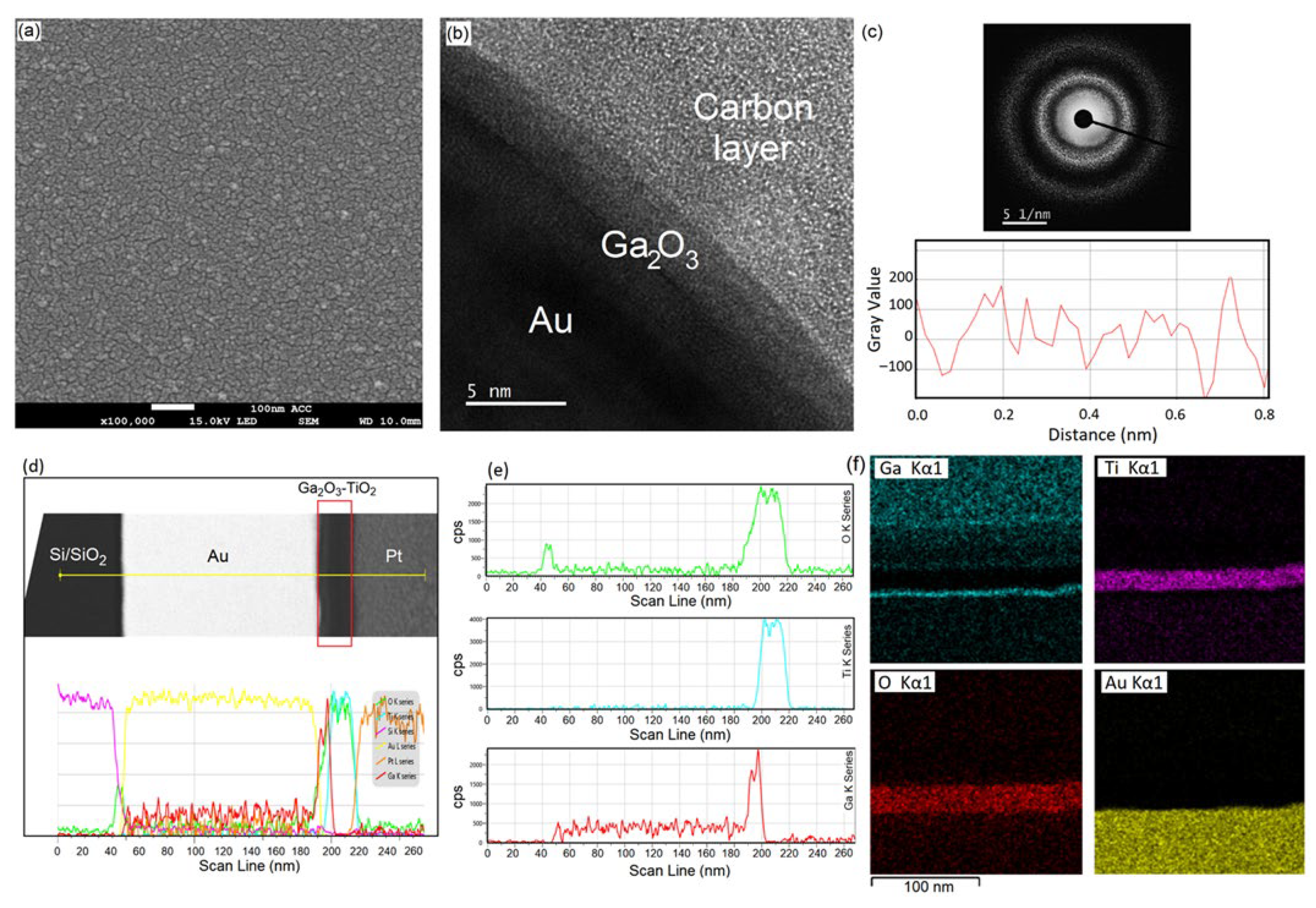
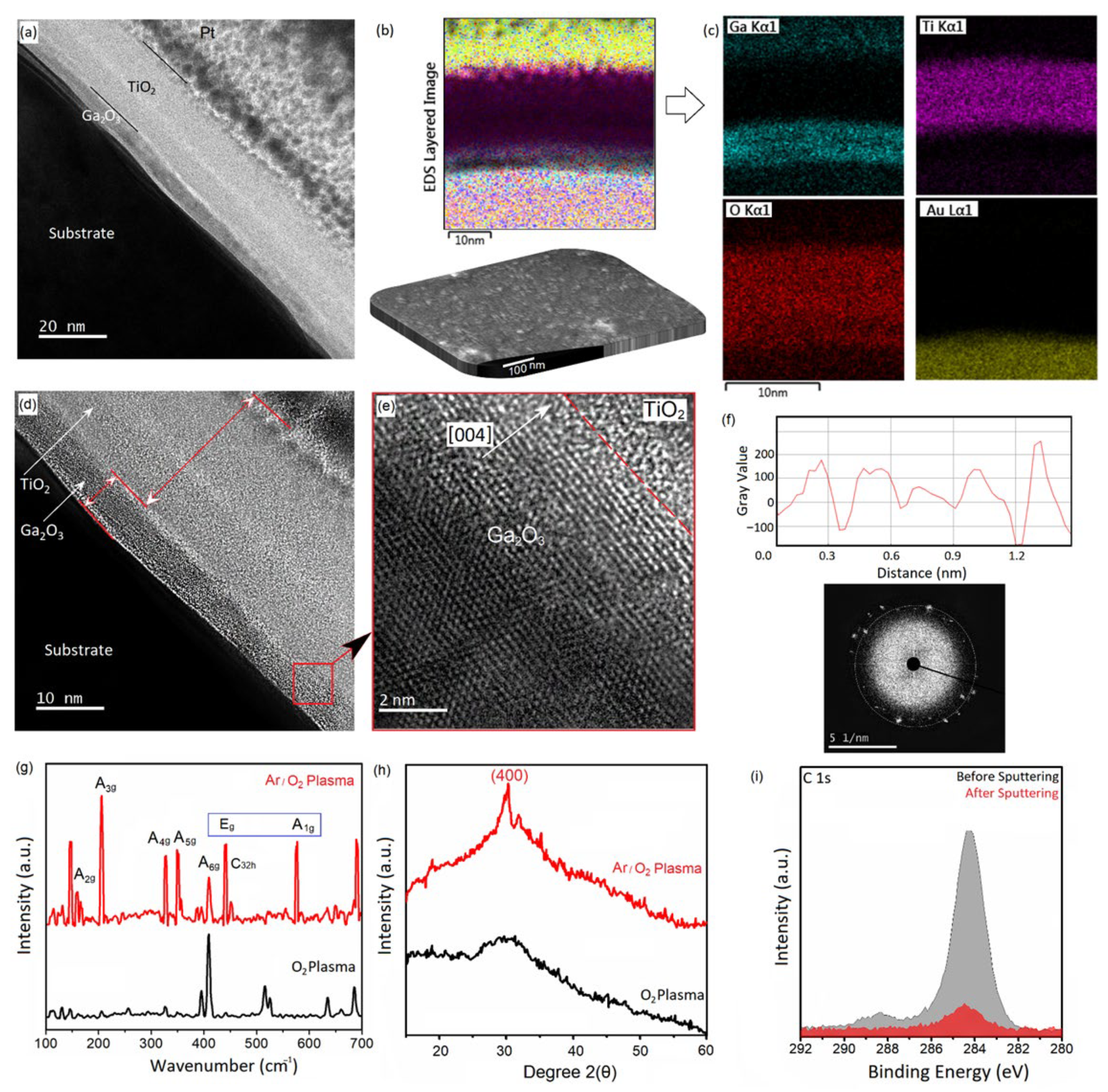
3.1. PE-ALD of Ga2O3 and TiO2

Figure 1a depicts the graphical scheme of the custom-made PE-ALD machine, where the ALD cycles and recipe are employed to deposit the Ga2O3 and TiO2 films. The ALD reactor was equipped with an in situ ellipsometer, turbo pump and inductively coupled with a 300 W plasma generator fed with ultra-high purity oxygen gas (UHP, O2) or Ar/O2 compound gases. Figure 1b depicts the molecular structure of the ALD precursor of gallium oxide. The partial pressure of the precursor was 200 mTorr, and the flow rate was 30 sccm. Two different gas compositions of pure O2 and a mixture of Ar and O2 (Ar/O2 = 4:1) were employed individually inside of the ALD chamber to investigate the effect the composition of gas has in the ALD process. Before each individual PE-ALD cycle, a 20 s wait time was included to reach to a stable conformal flow before using the plasma. A sequential residual flow of 20 s was employed in each individual stage. Figure 1c shows the saturation curves for the Ga2O3 precursor (Ga(TMHD)3) with constant O2 plasma exposure. The results showed that a pulse time of 1 s at a pressure of 0.003 mbar was sufficient to reach saturation growth under O2 plasma radiation (Figure 1c). It was observed that the growth rate was independent of the composition of the gas inside of the ALD chamber. The measured growth rate was 0.1 Å/cycle (Figure 1c). The inset in Figure 1c shows the typical linear increase of the Ga2O3 film thickness during 200 PE-ALD cycles. This constant growth rate was previously measured and reported for an entire temperature range between 100 °C and 400 °C, confirming a large PE-ALD window for this precursor and designed recipe [16]. The in situ ellipsometer recorded an increase in thickness of the Ga2O3 film vs. the number of PE-ALD cycles. We further investigated the thickness profile of as-deposited films on the surfaces of four-inch wafers after the PE-ALD process. These ellipsometry maps were collected at the incident angle of 65°. Figure 1d depicts the ellipsometry map of the Ga2O3 films after deposition on the Au substrate. The average thickness values of the Ga2O3 layer changed between 47.02 Å and 48.41 Å (Figure 1d), depicting a high level of controllability of the thickness in this ALD process. In the case of the Ga2O3 film, there was only a 2.6% difference in thickness over the area of the four-inch diameter wafer (Figure 1d). The ellipsometry map also showed the variations in thickness of the TiO2 film on the four-inch Au wafers (Figure 1g). In the case of TiO2 films, the thickness variations over 70% of the ALD film were less than 1.2% (Figure 1g). With the variable angle spectroscopy technique, we used four incident angles to investigate the changes in the polarization of lights that were reflected from the surfaces of the ALD films. These values were measured and expressed via two values of Ψ (Psi) and Δ (Delta) [28]. Figure 1e,f depict the variations of Ψ and Δ for the Ga2O3 film vs. the light wavelengths measured at four different incident angles of 60°, 65°, 70° and 75°. The same results for the TiO2 ALD film are presented in Figure 1h,i. It was observed that the practical values of Ψ and Δ were in high agreement with the predicted model (dashed black lines). The spectral dependencies of Ψ and Δ were fitted in the model to extract the film thickness using the least squares regression analysis and the weighted root mean square error (MSE) function. MSE described the difference between experimental data and model predicted data. The normal fit was based on Levenberg-Marquart regression algorithm to minimize the least squares difference between the experimental and model generated data [28]. Our fitted results showed that the MSE was 4.31 arbitrary units for the Ga2O3 film and 5.18 arbitrary units for the TiO2 layer, indicating a high level of consistency between the practical results and generated model data.
It was observed that the PE-ALD conditions directly affected the structure and properties of deposited Ga2O3 films. The ALD conditions resulted in the growth of either amorphous or crystalline structures. When the ALD process was conducted under O2 plasma atmosphere and at a low temperature of 150 °C, the extracted film was not crystalline. Figure 2a shows a typical FESEM image of the surface of Ga2O3 film a few nanometers thick on the Au substrate deposited under O2 plasma and at the ALD temperature of 150 °C. The FESEM study demonstrated an ultra-smooth film, which is the characteristics of amorphous ALD films before the annealing process. The TEM instrument was employed to investigate the regions of interest in the cross-sections. The cross-sectional TEM image from the heterointerface between the Au sublayer and Ga2O3 films depicted a sharp heterojunction with no clear indication of the crystalline structures (Figure 2b). The collected SAED patterns showed halo rings (Figure 2c). The diffraction patterns from an amorphous phase will be a ring pattern, but the rings will be rather diffuse (Figure 2c). Therefore, we estimate that this PE-ALD condition resulted in the growth of an amorphous Ga2O3 thin film. The measurement of the atomic interlayer distance did not show distinctive interlayer orders and arranged structures, confirming the non-crystalline nature of this ultra-thin Ga2O3 film (Figure 2c). After deposition of the TiO2 film, we analyzed the cross-sections of the Si/SiO2/Au/Ga2O3-TiO2 heterostructures with EDS equipment from a TEM machine. Figure 2d shows the cross-sectional views of the heterostructures accompanied by their corresponding EDS line elemental analysis. The detailed results of the EDS elemental line analyses showed the distribution of oxygen, titanium and gallium at the Ga2O3-TiO2 heterointerfaces (Figure 2e). The following EDS map analysis results in Figure 2f confirmed the growth of heterostructured Ga2O3-TiO2 films with distinguished sharp heterointerfaces. Furthermore, it was observed that the changes in the Ar/O2 composition at a constant ALD temperature of 150 °C did not affect the level of crystallinity of the as-deposited Ga2O3 films. In the present study, it was found that the ALD parameters had major impacts on the structures of the as-deposited Ga2O3 films a few nanometers thick. Here, it was observed that the increase in ALD temperature had a direct impact on the growth of the crystalline phases in the PE-ALD process.
Figure 3a shows the cross-sectional image of Au/Ga2O3-TiO2 heterostructures. A TEM study showed the distinguishable heterointerfaces between the Au substrate, Ga2O3 crystalline film and amorphous TiO2 structure. In this sample, an ALD temperature of 250 °C was employed during the deposition process of the Ga2O3 film under Ar/O2 plasma. The SEM image from the surface of the Ga2O3 film showed the growth of crystalline grains of Ga2O3 on the surface of the Au substrate. A tangible difference was observed between the surface morphology of this sample and the surface characteristics of the Ga2O3 film deposited at 150 °C and under pure O2 plasma (SEM images in Figure 3b vs. Figure 2a). The EDS analysis of the cross-section of the Au/Ga2O3-TiO2 heterointerfaces by TEM depicted the elemental distribution of the Ga, O, and Ti elements on the Au substrate (Figure 3c). It was observed that an increase in PE-ALD temperature did not affect the growth rate of the Ga2O3 film (0.1 Å/cycle). A wide ALD window was also observed previously in the PE-ALD process of Ga2O3 films by tris (2,2,6,6-tetramethyl-3,5-heptanedionato) gallium (III) or the [Ga(TMHD)3] precursor [16]. Via changing the ALD parameters, the structure of the Ga2O3 films considerably changed from an amorphous to a crystalline state. At the PE-ALD temperature of 250 °C and plasma gas composition of Ar/O2 = 4:1, fully crystalline Ga2O3 films grew on the Au substrate. The ellipsometry measurements showed a refractive index of 1.78 at an incident angle of 630 nm for this film. To compare the refractive index of as-deposited crystalline Ga2O3 films with the conventional annealed Ga2O3 nanostructures, we further operated rapid thermal annealing (RTA) on as-deposited amorphous Ga2O3 films and then measured the refractive index of these films. RTA was performed in an Ar atmosphere and at 550 °C for 5 min. A refractive index of 1.83 was measured for the annealed Ga2O3 film, which was a close number to the refractive index of the as-deposited crystalline Ga2O3 film of the present study. The refractive index of ultra-thin films can be affected by various factors, including stoichiometry, crystallinity and surface morphology. Since higher PE-ALD temperatures changed the level of crystallinity of the Ga2O3 films, it could be concluded that the ideal refractive index of as-deposited Ga2O3 film originated from a higher crystallinity level of this film (ALD temperature of 250 °C). We further measured the optical bandgap values of the as-deposited Ga2O3 films via the UV–Vis technique. The bandgap value of the film deposited at 150 °C was 4.5 eV, which was similar to the bandgap of the amorphous Ga2O3 film [29], while the measured bandgap of the as-deposited Ga2O3 film at 250 °C was 4.71 eV, which was a close number to the reported bandgap of the ß-Ga2O3 film [30]. Therefore, we used TEM equipment to generate high-resolution images from the heterointerface between the Ga2O3 and TiO2 films (Figure 3d). The Ga2O3 film was deposited at 250 °C, while the TiO2 film was deposited at 150 °C to gain an amorphous morphology of this oxide of titanium. Consequently, a clear heterointerface was detected at Au/Ga2O3-TiO2 junctions between the crystalline and amorphous structures (Figure 3e). The amorphous TiO2 is a functional material for application in a wide range of electronic and photonic devices. Metal/semiconductor heterojunctions play a fundamental role in a wide range of functional electronic and photonic systems, including RF electronics [31], metamaterials [32], memristors and artificial synaptic systems [33,34,35]. The heterointerface between the amorphous oxide structure and metal component plays a fundamental role in the performance of nanoelectronics systems. As an example, the junction between the Au plasmonic structure and amorphous TiO2 layer has witnessed a considerable charge trapping phenomenon due to the formation of a high Schottky barrier height at the heterointerfaces between the amorphous metal oxide semiconductor and Au-based components [36]. In this condition, the transfer of plasmonic-generated hot electrons from Au nanostructures to the TiO2 component of a semiconductor device is hindered at low applied voltages [6,36]. Therefore, the development of low-energy electronic systems faces technical challenges. To design tunable metal-semiconductor heterointerfaces with low-resistance characteristics, we aimed to develop a crystalline two-dimensional Ga2O3 electron channel layer between an amorphous TiO2 film and an Au sublayer. Figure 3e shows the atomic arrangement at the Ga2O3-TiO2 heterointerfaces. A clear crystalline pattern was observed in the Ga2O3 film with the interlayer distance of 0.3 nm, attributed to the (004) plane of ß-Ga2O3 [37]. The interlayer distance of the crystalline plane was also measured and is shown in Figure 3f, which was close to the value of ~0.3 nm. The collected SAED patterns by TEM probe showed a clear crystalline orientation, which was indexed as the (004) crystalline plane of ß-Ga2O3 [37] (Figure 3f).
To investigate the characteristics of the as-deposited Ga2O3 film, a Raman spectrometer was used to analyze the deposited ultra-thin films. Figure 3g depicts the Raman spectra of the Ga2O3 film deposited under pure O2 plasma (deposited at 150 °C) and the Raman spectra of the other Ga2O3 sample deposited under the mixed Ar/O2 gas with a 4:1 composition (deposited at 250 °C). The structure of the first sample was amorphous, while the second sample showed the highest level of crystallinity among all deposited samples. The Raman spectra of the as-deposited crystalline Ga2O3 film showed the characteristics of ß-Ga2O3. The A2g, A3g, A4g, A5g, A6g and C32h characteristic Raman peaks of ß-Ga2O3 are shown in Figure 3g. The Ag peaks at different Raman wavenumbers were caused by the vibration of lighter oxygen atoms perpendicular to the c-axis of crystalline ß-Ga2O3 [38,39]. The Raman peak at ~450 cm−1 was associated with the C32h space group of crystalline ß-Ga2O3. This peak specifically represented the bending of the GaO4 tetrahedral structure of ß-Ga2O3 [38]. Furthermore, two other peaks were distinguished at ~430 cm−1 and ~576 cm−1, attributed to the vibrational mode of the Ga atoms in α-Ga2O3 [40]. The obtained Raman modes from the crystalline film of Ga2O3 were in close agreement with the theoretical and experimental observations of previous studies [41]. Furthermore, the observation of the characteristic Raman modes of the α-Ga2O3 structure confirmed the presence of this polymorphous Ga2O3 in the composition of the thin films. These peaks were not detected in the Raman spectra of the Ga2O3 film deposited at 150 °C and under a pure O2 atmosphere of the plasma. We further investigated the structure of these two films by HRXRD. The XRD spectra of the Ga2O3 film deposited at 250 °C and under an Ar/O2 plasma atmosphere (4:1) showed an individual peak related to the (400) plane of ß-Ga2O3 [42]. These results were in harmony with the observed results of SAED patterns, confirming the growth of crystalline-stable ß-Ga2O3 films in these specific ALD conditions. The elemental compositions of the Ga2O3 films were also investigated to understand the effect of the ALD parameters on the quality of the as-deposited ALD films. Carbon was one of the main contaminants that might enter the structures of the ALD semiconductors from the organic ligands of the ALD precursors and, therefore, degrade the high quality of the ALD films. One of the main drawbacks of low-temperature ALD is the presence of residual carbon in ALD films. Therefore, high-resolution C 1s spectra were collected from the surfaces of the Ga2O3 films before and after Ar sputtering in the XPS test (Figure 3i). Despite the presence of atmospheric carbon contamination on the surfaces of ALD films, a trace of residual carbon was not found in any of the deposited films at 150 °C and 250 °C. This could confirm that O2 plasma successfully removed the metal organic ligands and their corresponding carbons during the ALD process. We also did not detect the presence of other contaminants in the XPS survey spectra of the ALD films.
Figure 4a shows the high-resolution Au 4f5/2 and Au 4f7/2 XPS peaks at the vicinity of 87 eV and 83 eV. These peaks were collected after the deposition of ~5 nm thick Ga2O3 films in different ALD conditions. It was observed that the Au 4f XPS peaks shifted to higher binding energies in the samples deposited under Ar/O2 plasma atmosphere and at the ALD temperature of 250 °C compared with those of the same samples deposited under O2 plasma at 150 °C. A positive shift was the indication of the development of different types of heterojunctions. The morphology of the Au substrates were the same in both samples; therefore, the shift in the core level of the Au 4f peak to a higher binding energy was evidence of a strong interaction between Au and the Ga2O3 thin films deposited under different ALD conditions. One can consider that the main difference between the film deposited under Ar/O2 plasma and the other Ga2O3 films (O2 plasma) was the presence of ionic defect sites of Ga in the film deposited under Ar/O2 [43]. Therefore, the shift of the Au 4f peak after deposition of a Ga2O3 film could be due to the presence of defect sites in the PE-ALD Ga2O3 film. Furthermore, it could be attributed to the rearrangement of the Au/Ga2O3 heterointerfaces in the crystalline states. The Ga2O3 films deposited under pure O2 plasma at 150 °C had amorphous structures, while the film deposited under pure O2 plasma at 250 °C had a crystalline structure. Therefore, the binding structure was totally different in these two cases. It was expected that the electron donation from the Ga2O3 side to the Au substrate was responsible for this shift of the Au 4f peaks to higher binding energies. We further investigated the Ga 3d peaks in these two samples to understand the possible interactions between Au and the Ga2O3 films. Figure 4b depicts the Ga 3d core-level spectra of the Ga2O3 films deposited by O2 and Ar/O2 plasma. The Ga3d peak shifted slightly to lower binding energies for the samples deposited under Ar/O2 plasma, which could be an indication of electron transfer between Au and the Ga2O3 films (Figure 4b). This could further support the previous concept of an electron transfer from the Ga2O3 films to the Au sublayer.
To investigate the oxidation state of the ALD films, the O 1s spectra were collected and are shown in Figure 4c. The O 1s core level was deconvoluted into two components. The peak at 530.4 eV (upper graph) was attributed to the Ga-O bonds in the Ga2O3 lattice. This peak represented the number of oxygen atoms surrounding the oxidized gallium atoms in the lattice of Ga2O3. The other peak at 531.2 eV belonged to the oxygen vacancies in the Ga2O3 lattice, representing the oxygen deficiency within the Ga2O3 matrix [44]. It was observed that the position of these peaks shifted to different binding energies at different ALD conditions, representing the effect of O2 or Ar/O2 plasma on the formation energy of Ga-O bonds in the ALD films. The shift in the positions of these peaks toward lower or higher binding energies, relative to those of other Ga2O3 films, could originate from differences in stoichiometry, nature and the degree of interactions among various species of thin films. The investigation on the O 1s XPS spectra of these films showed that the film deposited under Ar/O2 plasma had a higher level of oxygen vacancies (Figure 4c). It was possible that deposition under an Ar/O2 atmosphere induced a higher level of Ga3+ with an associated increase in the oxygen vacancies, especially on the surfaces of the ultra-thin Ga2O3 films. We further investigated the Ti 2p peaks after the deposition of the TiO2 film on the amorphous and crystalline Ga2O3 films. Figure 4d depicts the Ti 2p peaks of the Ga2O3-TiO2 and ß-Ga2O3-TiO2 heterostructures fabricated at different plasma atmospheres. The study of the XPS spectra of heterostructured Ga2O3-TiO2 films showed a gradual shift in the Ti 2p peaks to higher binding energies after deposition of the TiO2 film on crystalline ß-Ga2O3. The crystalline ß-Ga2O3 film was deposited under Ar/O2 plasma at 250 °C. This gradual shift of the Ti 4f peaks was evidence of an electron exchange between the crystalline Ga2O3 and TiO2 films (Figure 4d).
We further investigated the light–matter interactions in the as-deposited Ga2O3 films. Figure 4e depicts the calculated bandgap of the ß-Ga2O3-TiO2 films, which was extracted from the outcomes of the UV–Vis measurements. A bandgap of 3.35 eV was attributed to the TiO2 film, while a bandgap of 4.71 eV was characteristic of the ß-Ga2O3 film [45,46]. We further investigated the PL spectra of the ß-Ga2O3 film to better understand the photonic properties of the as-deposited crystalline ß-Ga2O3 film. The typical PL spectra of the as-deposited ß- Ga2O3 films are shown in Figure 4f. The PL spectra were characterized by several peaks from the UV to visible and near infrared regions (UV–Vis). Two sharp peaks were centered at ~291 nm and ~378 nm of the UV region, and two other peaks were centered at ~442 nm and ~474.1 nm in the blue regions (Figure 4f). A singular peak was also detected at 542.0 nm in the green region of the spectrum, and another peak was also distinguishable at 619.9 nm in the red regions. The relative intensity of the green luminescence was considerably higher than that of the peaks at the blue and red regions (Figure 4f). The PL emission could be attributed to the transition of an electron from the donor band to the acceptor and valance bands of Ga2O3 [47]. In the PL spectra of Figure 4f, the major emission bands were detected at 378.0 nm (L1, 3.2 eV), 442.0 nm (L2, 2.8 eV), 474.0 nm (L3, 2.60 eV), 542.0 nm (L4, 2.20 eV) and an individual peak at ~291.0 nm (L5, 4.26 eV). The detection of UV emission in the ß-Ga2O3 film could be explained by a model that suggested the electron and holes could be de-trapped due to photoexcitation [48,49]. The migration and incidence of these electron/hole pairs formed self-trapped excitons. These excitons recombined and emitted UV photons [47,48]. A similar mechanism for UV emission was previously reported for nanostructured ß-Ga2O3 [49,50]. The UV–green emission in the ß-Ga2O3 structure was related to the recombination of an electron on the donor band of Ga2O3 with another hole formed in the acceptor band of this material [51]. The oxygen vacancies and Ga2+ formed a donor band, while the acceptor band was formed by a gallium vacancy and pairs of gallium–oxygen vacancy [48]. A simplified model was extracted from the PL spectra of the ß-Ga2O3 film of the present study and is shown in Figure 4f. The donor band (E1) was located 0.04 eV below the conduction band minimum (CBM), which was attributed to the formed oxygen vacancies [48,49,50]. The electron photoexcitation from the conduction band to the valence band was accompanied by the electron relaxation, where the electron could freely move from the conduction band to the donor band before the occurrence of the radiative recombination phenomenon. The following electron/hole recombination between the donor and acceptor bands yielded the generation of UV–green emission in the PL spectra of the ultra-thin ß-Ga2O3 films (Figure 4f). The corresponding analysis of the energy levels in the bandgap of ß-Ga2O3 is presented in the following lines and is depicted in Figure 4f.
E (L1) − E (L2) = 0.4 eV
E (L3) − E (L4) = 0.4 eV
E (L1) − E (L3) = 0.6 eV
E (L2) − E (L4) = 0.6 eV
Eg (4.7 eV) − E1 − E2 = 4.26 eV
The calculated value in (5) was equal to 4.26 eV, which was consistent with the energy level of the detected peak at ~291 nm. This emission was related to the recombination of electrons in the donor band with the holes in the valence band edge [48]. The red emission at 619.9 eV could be attributed to the Au substrate and its coupling with the ß-Ga2O3 semiconductor film. The PL spectra of the ß-Ga2O3-TiO2 heterostructure also showed two characteristic peaks in the UV regions (Figure 4g). To investigate the type of conductivity of the as-deposited ß-Ga2O3 film by the Hall-Effect measurement technique, the samples were studied at various current ranges, and the results are presented in Figure 4h. The Hall coefficient values experienced a sharp decline from positive values to negative values when the applied current increased and then remained constant for a wide range of applied currents, with slight changes. This observation was evidence of p-type conductivity, which was the characteristic property of the ß-Ga2O3 film in the present study [26]. The study on the valence band maximum (VBM) of the ALD films presented valuable information on the electronic characteristics of the ALD films (Figure 4i). Our studies showed that the Ga2O3 film developed at 150 °C and under pure O2 plasma had the VBM value of 0.49 eV, while the VBM of the ß-Ga2O3 film deposited at 250 °C and under Ar/O2 plasma was −0.24 eV. This negative VBM indicated the presence of energy states extruding deeper in the band energy of the ß-Ga2O3 film and was an indication of the p-type conductivity of this film [26,51]. We further studied the VBM of the heterostructured films. It was found that the remarkable difference in the VBM values of the ß-Ga2O3 and TiO2 films resulted in the shift of VBM of the Ga2O3-TiO2 metal-oxide heterojunctions into lower values in the ß-Ga2O3-TiO2 heterostructured films. This was more evidence of the formation of the p-n junction at 2D heterointerfaces between p-type Ga2O3 and n-type TiO2 films. Therefore, the correct materials selection and well-designed fabrication process let us develop a sharp 2D crystalline channel between Au and the amorphous TiO2 film. In this structure, the atomic-scale thin p-type interlayer ß-Ga2O3 film acted as the electron polarization channel. The impediment studies resulted in insights into the heterointerface resistance at the Au/Ga2O3-TiO2 junction. Figure 4j depicts the results of the impedance measurements of the Ga2O3 and Ga2O3-TiO2 heterojunctions. The Ga2O3 film deposited at 150 °C and under O2 plasma showed a larger Nyquist semicircle plot with a measured Ret of ~1550 Ω, while the Ga2O3 film deposited at 250 °C and under Ar/O2 plasma atmosphere showed a lower value of 1267 Ω (Figure 4j). It is believed that the higher level of crystallinity of ß-Ga2O3 was responsible for the lower resistance at the Au/ß-Ga2O3 heterointerfaces. Table 1 provides detailed information on the ALD conditions and properties of the developed all-oxide heterostructured films.

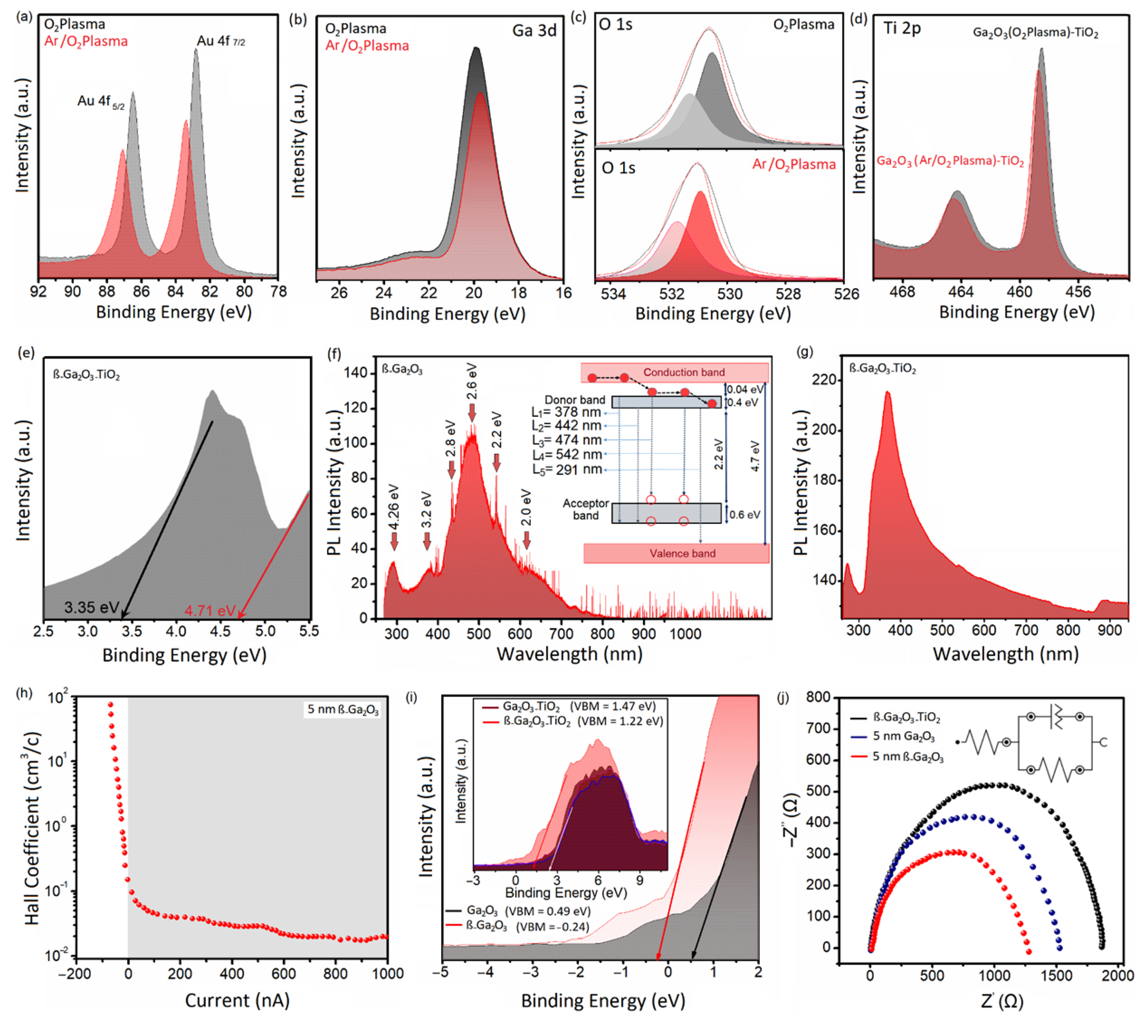
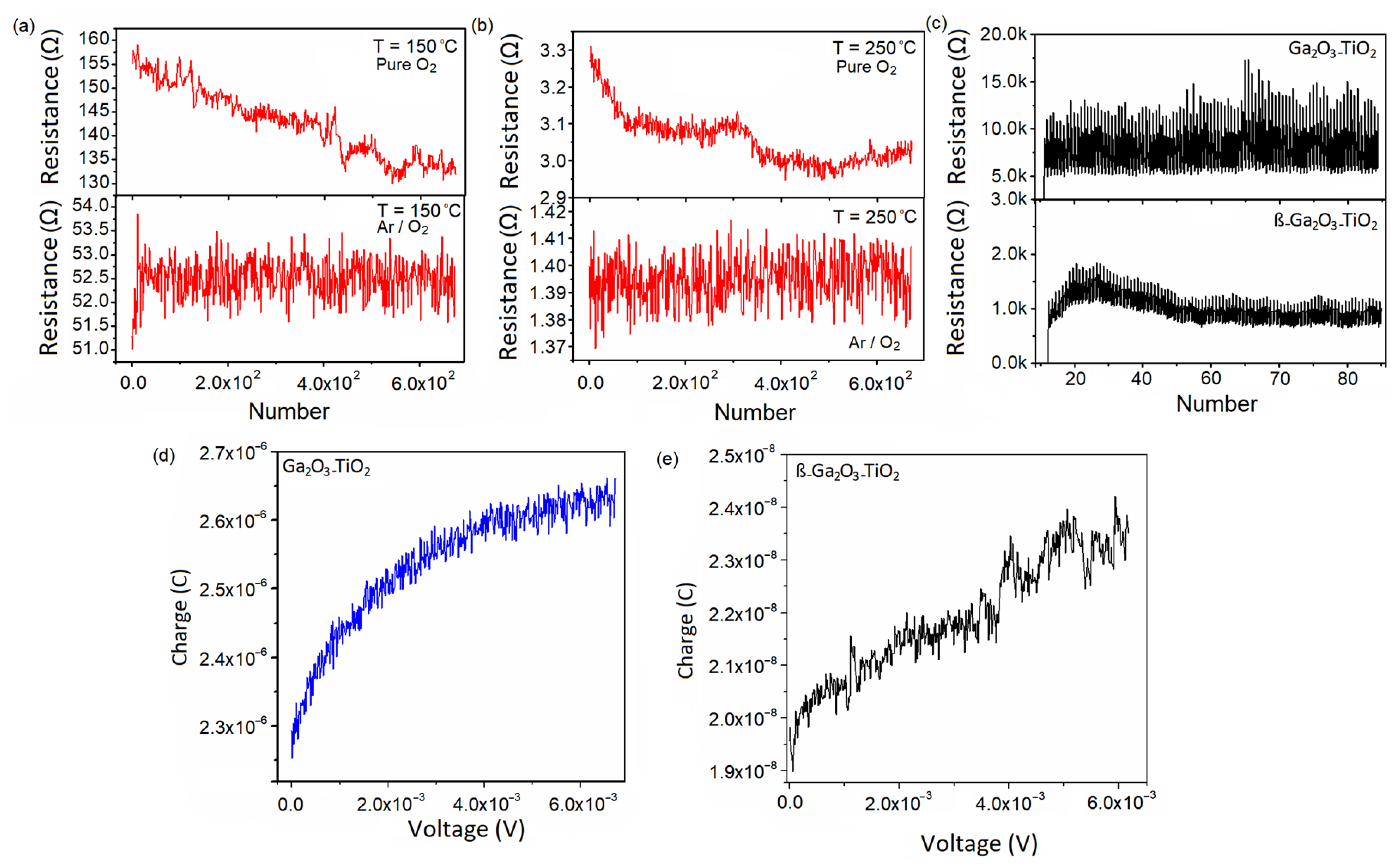
3.2. Photoelectrical Characteristics

To investigate the electrical properties of the as-deposited films, a series of high-frequency photoelectrical measurements were designed and performed. Figure 5a,b show the photoresistance properties of the Au/Ga2O3 heterointerfaces. The Ga2O3 films were deposited under O2 and Ar/O2 plasma at different ALD temperatures of 150 °C and 250 °C. A constant 0.1 volt driving force was employed to measure the photoconductance fluctuations at the heterointerfaces of the Au/Ga2O3 films. To this aim, a λ = 750 nm near-infrared laser was used to generate light pulses with a frequency of 100 Hz. The films deposited at higher temperatures in the ALD had lower heterointerface resistance values. This observation was attributed to the higher level of crystallinity of the Ga2O3 films deposited at higher ALD temperatures. The following measurements of high-frequency resistance at the Au/Ga2O3-TiO2 heterojunction confirmed that the Au/ß-Ga2O3-TiO2 junction showed considerably lower heterointerface resistance (Figure 5c). The typical interface resistance value of the Au/Ga2O3-TiO2 heterojunction was almost 10 times higher than that of the Au/ß-Ga2O3-TiO2 heterostructures at a frequency of 100 Hz (V = 0.1 V). The increased crystallinity enhanced the conductance of the ultra-thin Ga2O3 films, and therefore, the ß-Ga2O3 film acted as the ultra-thin gate channel at the heterointerface between the Au underlayer and amorphous TiO2 structure. Moreover, the p-type nature of the ß-Ga2O3 film was an important factor for the polarization of the electron–hole pairs at the Ga2O3-TiO2 heterojunction. The p-type conductivity of the developed ß-Ga2O3 film enabled the facile and fast separation of the charge carriers at the Au/TiO2 heterointerfaces and, therefore, suppressed the charge trapping at the Au and amorphous TiO2 films. When the Au/TiO2 heterointerface was equipped with the crystalline ß-Ga2O3 film, the electron–hole pairs were separated faster due to the formation of the p-n junction and moved faster to the adjacent components due to the lower resistance of the crystalline ß-Ga2O3 channel. Moreover, it was observed that the type of heterointerface considerably affected the number of trapped charges at the Au/Ga2O3-TiO2 heterointerfaces. The values of the trapped charges at a typical Au/Ga2O3-TiO2 heterojunction were almost 100 times higher than that of the Au/ß-Ga2O3-TiO2 heterostructure (Figure 5d,e). The lower number of trapped charges at the metal/semiconductor heterointerfaces could be attributed to the lower resistance of the ß-Ga2O3 electron channels and their higher polarization capabilities due to the p-type nature of these ultra-thin crystalline layers. Generally speaking, our observations showed that the ALD-developed ultra-thin ß-Ga2O3 film could sufficiently decrease the heterointerface resistance in metal-semiconductor heterointerfaces and facile the charge carrier separation at the developed p-n junction. Therefore, the developed PE-ALD technique is a capable approach for the design of tunable 2D heterointerfaces in nanofabrication technologies.

4. Conclusions

The PE-ALD technique was employed to develop an ultra-thin crystalline Ga2O3 film at a metal/semiconductor heterointerface to improve the high-frequency electrical performance of Au/TiO2-based devices. It was observed that the ALD parameters, including the ALD temperature and plasma gas composition, had considerable impact on the structures of the ultra-thin Ga2O3 films. It was observed that a decrease in the generated atomic oxygen in the ALD plasma had a direct effect on the formation of a thermodynamically stable ß-Ga2O3 phase. Therefore, the 5-nm-thick stable ß-Ga2O3 films were developed during the PE-ALD process under Ar/O2 plasma with a ratio of 4:1. The ALD temperature also had a direct impact on the level of crystallinity of the Ga2O3 films, where the ALD film deposited at 150 °C was totally amorphous while the Ga2O3 film developed at 250 °C showed crystalline characteristics. Consequently, the ultra-thin p-type ß-Ga2O3 film was deposited at 250 °C and under Ar/O2 plasma to develop the electron channel layer at the Au/ß-Ga2O3-TiO2 heterojunctions. This ultra-thin polarized heterointerface showed a distinguished performance as a low-energy heterointerface barrier for high-frequency electronic devices. This ALD approach for the design and fabrication of a self-polarized ultra-thin election channel layer could be expanded to the design and development of various types of heterojunctions and tunable photonic heterointerfaces for a wide range of functional applications in low-power semiconductor devices.

Author Contributions

Introduction of the concept, experiments and original draft preparation, M.K.A. and N.S.L. Supervision, S.Z. All authors have read and agreed to the published version of the manuscript.

Funding

This research was funded by Ghent University Global Campus (Republic of Korea).

Institutional Review Board Statement

Not applicable.

Informed Consent Statement

Not applicable.

Data Availability Statement

Available on request from the authors.

Acknowledgments

This work was supported by a research program from Ghent University Global Campus, Republic of Korea.

Conflicts of Interest

The authors declare no conflict of interest.

References

  1. Xu, H.; Karbalaei Akbari, M.; Zhuiykov, S. 2D semiconductor nanomaterials and heterostructures: Controlled synthesis and functional applications. Nanoscale Res. Lett. 2021, 16, 94. [Google Scholar] [CrossRef] [PubMed]
  2. Zhou, X.; Jiang, D.; Zhao, M.; Wang, N.; Duan, Y.; Wang, W.; Li, M.; Li, Q.; Shan, C.; Sun, J. Polarization induced two-dimensional electron gas in ZnO/ZnMgO heterointerface for high-performance enhanced UV photodetector. J. Alloys Compd. 2020, 820, 153416. [Google Scholar] [CrossRef]
  3. Li, D.; Huang, X.; Xiao, Z.; Zhang, L.; Hao, Y.; Song, J.; Shao, D.-F.; Tsymbal, E.Y.; Tsymbal, E.Y.; Hong, X. Polar coupling enabled nonlinear optical filtering at MoS2/ferroelectric heterointerfaces. Nat. Commun. 2020, 11, 1422. [Google Scholar] [CrossRef] [PubMed] [Green Version]
  4. Niu, W.; Wang, X.; Xu, Y.; Zhang, R. Recent advances on spin-polarized two-dimensional electron gases at oxide interfaces. ACS Appl. Electron. Mater. 2021, 3, 128–144. [Google Scholar] [CrossRef]
  5. Ummethala, S.; Harter, T.; Koehnle, K. THz-to-optical conversion in wireless communications using an ultra-broadband plasmonic modulator. Nat. Photonics 2019, 13, 519–524. [Google Scholar] [CrossRef] [Green Version]
  6. Karbalaei Akbari, M.; Hai, Z.; Wei, Z.; Detavernier, C.; Solano, E.; Verpoort, F.; Zhuiykov, S. ALD-Developed plasmonic two-dimensional Au–WO3–TiO2 heterojunction architectonics for design of photovoltaic devices. ACS Appl. Mater. Interfaces 2018, 10, 10304–10314. [Google Scholar] [CrossRef]
  7. Xu, H.; Karbalaei Akbari, M.; Verpoort, F.; Zhuiykov, S. Nano-engineering and functionalization of hybrid Au–MexOy–TiO2 (Me = W, Ga) hetero-interfaces for optoelectronic receptors and nociceptors. Nanoscale 2020, 12, 20177–20188. [Google Scholar] [CrossRef]
  8. Wu, P.; Appenzeller, J. Toward CMOS like devices from two-dimensional channel materials. APL Mater. 2019, 7, 100701. [Google Scholar] [CrossRef] [Green Version]
  9. Karbalaei Akbari, M.; Zhuiykov, S. Photonic and plasmonic devices based on two-dimensional semiconductors. In Ultrathin Two-Dimensional Semiconductors for Novel Electronic Applications; CRC Press Tylor and Francis: Boca Raton, FL, USA, 2020; Volume 1, pp. 145–169. [Google Scholar]
  10. Zaidi, S.J.A.; Basit, M.B.; Park, T.J. Advances in atomic layer deposition of metal sulfides: From a precursors perspective. Chem. Mater. 2022, 34, 7106–7138. [Google Scholar] [CrossRef]
  11. Zhuiykov, S.; Karbalaei Akbari, M.; Hai, Z.; Xue, C.; Xu, H.L. Wafer-scale fabrication of conformal atomic-layered TiO2 by atomic layer deposition using tetrakis (dimethylamino) titanium and H2O precursors. Mat. Des. 2017, 120, 99–108. [Google Scholar] [CrossRef]
  12. Xu, H.; Karbalaei Akbari, M.; Hai, Z.; Wei, Z.; Hyde, L.; Verpoort, F.; Xue, C.; Zhuiykov, S. Ultra-thin MoO3 film goes wafer-scaled nano-architectonics by atomic layer deposition. Mat. Des. 2018, 149, 135–144. [Google Scholar] [CrossRef]
  13. Karbalaei Akbari, M.; Hu, J.; Verpoort, F.; Lu, H.; Zhuiykov, S. Nanoscale all-oxide-heterostructured bio-inspired optoresponsive nociceptor. Nano-Micro Lett. 2020, 12, 83. [Google Scholar] [CrossRef] [PubMed] [Green Version]
  14. Keskiväli, L.; Heikkilä, P.; Kenttä, E.; Virtanen, T.; Rautkoski, H.; Pasanen, A.; Vähä-Nissi, M.; Putkonen, M. Comparison of the Growth and Thermal Properties of Nonwoven Polymers after Atomic Layer Deposition and Vapor Phase Infiltration. Coatings 2021, 11, 1028. [Google Scholar] [CrossRef]
  15. Hai, Z.; Karbalaei Akbari, M.; Xue, C.; Xu, H.; Hyde, L.; Zhuiykov, S. Wafer-scaled monolayer WO3 windows ultra-sensitive, extremely-fast and stable UV-A photodetection. Appl. Surf. Sci. 2017, 405, 169–177. [Google Scholar] [CrossRef]
  16. Ramachandran, R.; Dendooven, J.; Botterman, J.; Sree, S.P.; Poelman, D.; Martens, J.; Poelman, H.; Detavernier, C. Plasma enhanced atomic layer deposition of Ga2O3 thin films. J. Mater. Chem. A 2014, 2, 19232–19238. [Google Scholar] [CrossRef]
  17. Lopa, N.S.; Karbalaei Akbari, M.; Wu, D.; Verpoort, F.; Zhuiykov, S. Two-dimensional SnO2-ZnO nanohybrid electrode fabricated via atomic layer deposition for electrochemical supercapacitors. Energy Fuels 2023, 37, 3142–3151. [Google Scholar] [CrossRef]
  18. Altuntas, H.; Donmez, I.; Ozgit-Akgun, C.; Biyikli, N. Electrical characterization of β-Ga2O3 thin films grown by PEALD. J. Alloys Compd. 2014, 593, 190–195. [Google Scholar] [CrossRef] [Green Version]
  19. Knoops, H.; Faraz, T.; Arts, K.; Kessels, W.M.M. Status and prospects of plasma-assisted atomic layer deposition. J. Vac. Sci. Technol. A 2019, 37, 030902. [Google Scholar] [CrossRef] [Green Version]
  20. Donmez, I.; Ozgit-Akgun, C.; Biyikli, N. Low Temperature deposition of Ga2O3 thin films using trimethylgallium and oxygen plasma. J. Vac. Sci. Technol. A 2013, 31, 01A110. [Google Scholar] [CrossRef]
  21. Comstock, D.J.; Elam, J.W. Atomic layer deposition of Ga2O3 films using trimethylgallium and ozone. Chem. Mater. 2012, 24, 4011–4018. [Google Scholar] [CrossRef]
  22. Wheeler, V.D.; Nepal, N.; Boris, D.R.; Qadri, S.B.; Nyakiti, L.O.; Lang, A.; Koehler, A.; Foster, G.; Walton, S.G.; Eddy, C.R.; et al. Phase control of crystalline Ga2O3 films by plasma-enhanced atomic layer deposition. J. Chem. Mater. 2020, 32, 1140–1152. [Google Scholar] [CrossRef]
  23. Karbalaei Akbari, M.; Zhuiykov, S. Atomic layer deposition of two-dimensional semiconductors. In Ultrathin Two-Dimensional Semiconductors for Novel Electronic Applications; CRC Press Tylor and Francis: Boca Raton, FL, USA, 2020; Volume 1, pp. 43–73. [Google Scholar]
  24. Playford, H.Y.; Hannon, A.C.; Barney, E.R.; Walton, R.I. Structures of Uncharacterized Polymorphs of Gallium Oxide from Total Neutron Diffraction. Chem. Eur. J. 2013, 19, 2803–2813. [Google Scholar] [CrossRef] [PubMed]
  25. Cora, I.; Mezzadri, F.; Boschi, F.; Bosi, M.; Caplovicova, M.; Calestani, G.; Dodony, I.; Pecz, B.; Fornari, R. The real structure of ε-Ga2O3 and its relation to κ-phase. CrystEngComm 2017, 19, 1509–1516. [Google Scholar] [CrossRef] [Green Version]
  26. Chikoidze, E.; Fellous, A.; Perez-Tomas, A.; Sauthier, G.; Tchelidze, T.; Ton-That, C.; Thanh Huynh, T.; Phillips, M.; Russell, S.; Jennings, M.; et al. P-type β-gallium oxide: A new perspective for power and optoelectronic devices. Mat. Today Phys. 2017, 3, 118–126. [Google Scholar] [CrossRef] [Green Version]
  27. Fujita, S.; Oda, M.; Kaneko, K.; Hitora, T. Evolution of corundum-structured III-oxide semiconductors: Growth, properties, and devices. Jpn. J. Appl. Phys. 2016, 55, 1202A3. [Google Scholar] [CrossRef] [Green Version]
  28. Zhuiykov, S.; Karbalaei Akbari, M.; Hai, Z.; Xue, C.; Xu, H.; Hyde, L. Data set for fabrication of conformal two-dimensional TiO2 by atomic layer deposition using tetrakis (dimethylamino) titanium (TDMAT) and H2O precursors. Data Br. 2017, 13, 401–407. [Google Scholar] [CrossRef]
  29. Karbalaei Akbari, M.; Verpoort, F.; Zhuiykov, S. Plasma-enhanced elemental enrichment of liquid metal interfaces: Towards realization of GaS nanodomains in two-dimensional Ga2O3. Appl. Mater Today 2022, 27, 101461. [Google Scholar] [CrossRef]
  30. Yao, Y.; Okur, S.; Lyle, L.A.M.; Tompa, G.S.; Salagaj, T.; Sbrockey, N.; Davis, R.F.; Porter, L.M. Growth and characterization of α-, β-, ε-phases of Ga2O3 using MOCVD and HVPE techniques. Mater. Res. Lett. 2018, 6, 268–275. [Google Scholar] [CrossRef] [Green Version]
  31. Mahi, A.; Mahi, F.Z.; Abbes, A. Systematic analysis of semiconductor photoconductivity dynamics under different laser excitations: Two- and three-level models. J. Comput. Electron 2023, 22, 296–309. [Google Scholar] [CrossRef]
  32. Naik, G.V.; Boltasseva, A. A comparative study of semiconductor-based plasmonic metamaterials. Metamaterials 2011, 5, 1–7. [Google Scholar] [CrossRef] [Green Version]
  33. Xu, H.; Karbalaei Akbari, M.; Wang, S.; Chen, S.; Kats, E.; Verpoort, F.; Hue, J.; Zhuiyko, S. Tunability of near infrared opto-synaptic properties of thin MoO3 films fabricated by atomic layer deposition. Appl. Surf. Sci. 2022, 539, 153399. [Google Scholar] [CrossRef]
  34. Karbalaei Akbari, M.; Ramachandran, R.K.; Detavernier, C.; Hu, J.; Kim, J.; Verpoort, F.; Zhuiykov, S. Heterostructured plasmonic memristors with tunable optosynaptic functionalities. J. Mater. Chem. C 2021, 9, 2539–2549. [Google Scholar] [CrossRef]
  35. Salonikidou, B.; Yasunori, T.; Le Borgne, B.; England, J.; Shizuo, T.; Sporea, R.A. Toward fully printed memristive elements: a-TiO2 electronic synapse from functionalized nanoparticle ink. ACS Appl. Electron. Mater. 2019, 1, 2692–2700. [Google Scholar] [CrossRef]
  36. Zhuiykov, S.; Karbalaei Akbari, M. Metal/semiconductor hetero-interface engineering for photocurrent controlling in plasmonic photodetectors. In Proceedings of the SMSI 2021—Sensors and Instrumentation, Online, 3–6 May 2021; AMA Service Gmbh: Nuremberg, Germany, 2021; pp. 165–166. [Google Scholar]
  37. Auer, E.; Lugstein, A.; Loffler, S.; Hyun, Y.J.; Brezna, W.; Bertagnolli, E.; Pongratz, P. Ultrafast VLS growth of epitaxial β-Ga2O3 nanowires. Nanotechnology 2009, 20, 434017. [Google Scholar] [CrossRef] [PubMed]
  38. Phumying, S.; Labauyai, S.; Chareonboon, W.; Phokha, S.; Maensiri, S. Optical properties of β-Ga2O3 nanorods synthesized by a simple and cost-effective method using egg white solution. Jpn. J. Appl. Phys. 2015, 54, 06FJ13. [Google Scholar] [CrossRef]
  39. Cuscó, R.; Domènech-Amador, N.; Hatakeyama, T.; Yamaguchi, T.; Honda, T.; Artús, L. Lattice dynamics of a mistchemical vapor deposition-grown corundum-like Ga2O3 single crystal. J. Appl. Phys. 2015, 117, 185706. [Google Scholar] [CrossRef]
  40. Xu, Y.; Zhang, C.; Cheng, Y.; Li, Z.; Cheng, Y.N.; Feng, Q.; Chen, D.; Zhang, J.; Hao, Y. Influence of carrier gases on the quality of epitaxial corundum-structured α-Ga2O3 films grown by mist chemical vapor deposition method. Materials 2019, 12, 3670. [Google Scholar] [CrossRef] [Green Version]
  41. Kranert, C.; Sturm, C.; Schmidt-Grund, R. Raman tensor elements of β-Ga2O3. Sci. Rep. 2016, 6, 35964. [Google Scholar] [CrossRef] [Green Version]
  42. Sharma, A.; Varshney, M.; Saraswat, H.; Chaudhary, S.; Parkash, J.; Shin, H.-J.; Chae, K.-H.; Won, S.-O. Nano-structured phases of gallium oxide (GaOOH, α-Ga2O3, β-Ga2O3, γ-Ga2O3, δ-Ga2O3, and ε-Ga2O3): Fabrication, structural, and electronic structure investigations. Int. Nano Lett. 2020, 10, 71–79. [Google Scholar] [CrossRef]
  43. Achoura, A.; Islamb, M.; Solaymanic, S.; Vizireanud, S.; Saeede, K.; Dinescu, G. Influence of plasma functionalization treatment and gold nanoparticles on surface chemistry and wettability of reactive-sputtered TiO2 thin films. Appl. Surf. Sci. 2018, 458, 678–685. [Google Scholar] [CrossRef]
  44. Wang, Y.; Li, N.; Duan, P.; Sun, X.; Chu, B.; He, Q. Properties and photocatalytic activity of 𝛽-Ga2O3 nanorods under simulated solar irradiation. J. Nanomater. 2015, 16, 126. [Google Scholar]
  45. Shi, F.; Han, J.; Xing, Y.; Li, J.; Zhang, L.; He, T.; Li, T.; Deng, X.; Zhang, X.; Zhang, B. Annealing effects on properties of Ga2O3 films deposited by plasma-enhanced atomic layer deposition. Mater. Lett. 2019, 237, 105–108. [Google Scholar] [CrossRef]
  46. Passlack, M.; Schubert, E.F.; Hobson, W.S.; Hong, M.; Moriya, N.; Chu, S.N.G.; Konstadinidis, K.; Mannaerts, J.P.; Schnoes, M.L.; Zydzik, G.J. Ga2O3 films for electronic and optoelectronic applications. J. Appl. Phys. 1995, 77, 686–693. [Google Scholar] [CrossRef]
  47. Remple, C.; Huso, J.; McCluskey, M.D. Photoluminescence and Raman mapping of β-Ga2O3. AIP Advances 2021, 11, 105006. [Google Scholar] [CrossRef]
  48. Mi, W.; Luan, C.; Li, Z.; Zhao, C.; Feng, X.; Ma, J. Ultraviolet–green photoluminescence of ß-Ga2O3 films deposited on MgAl6O10 (100) substrate. Opt. Mater. 2013, 35, 2624–2628. [Google Scholar] [CrossRef]
  49. Hao, J.H.; Cocivera, M. Optical and luminescent properties of undoped and rare-earth-doped Ga2O3 thin films deposited by spray pyrolysis. J. Phys. D: Appl. Phys. 2002, 35, 433. [Google Scholar] [CrossRef]
  50. Lorenz, M.R.; Woods, J.F.; Gambino, R.J. Some electrical properties of the semiconductor β-Ga2O3. J. Phys. Chem. Solids 1967, 28, 403. [Google Scholar] [CrossRef]
  51. Chikoidze, E.; Sartel, C.; Mohamed, H.; Madaci, I.; Tchelidze, T.; Modreanu, M.; Vales-Castro, P.; Rubio, C.; Arnold, C.; Sallet, V.; et al. Enhancing the intrinsic p-type conductivity of the ultra-wide bandgap Ga2O3 semiconductor. J. Mater. Chem. C 2019, 7, 10231–10239. [Google Scholar] [CrossRef]
Figure 1. (a) The graphical scheme of the ALD machine. (b) The 3D chemical structure of C33H57GaO6. (c) The graph of growth per cycle vs. the pulse time of ALD. The inset shows the variations in thickness vs. the number of ALD cycles. (d) The ellipsometry map depicting the thickness of the Ga2O3 film on 4 inch diameter wafers. (e,f) Variable angle spectral ellipsometry data for Ga2O3. (g) The ellipsometry map depicting the thickness of the TiO2 film on 4-inch-diameter wafers. (h,i) Variable angle spectral ellipsometry data for TiO2.
Coatings 13 01041 g001
Figure 2. (a) The FESEM image from the surface of a Ga2O3 film. (b) The cross-sectional TEM image from the Au/Ga2O3-TiO2 heterojunction. (c) A graph of the interlayer distance accompanied by the SAED patterns of a Ga2O3 film. (d) The cross-sectional TEM image. Red box represents Ga2O3-TiO2 (e) Elemental EDS line analysis of the heterojunction. (f) A detailed elemental EDS map of the Au/Ga2O3-TiO2 heterojunction. The sample was deposited at 150 °C and under pure O2 plasma.
Coatings 13 01041 g002
Figure 3. (a) A cross-sectional image of the Au/Ga2O3-TiO2 heterojunction. (b) The SEM image of the surface of a crystalline Ga2O3 film accompanied by the cross-sectional EDS map of the Au/Ga2O3-TiO2 heterojunction. (c) A detailed elemental EDS map of the Au/Ga2O3-TiO2 heterojunction. (d) A cross-sectional TEM image from the Au/Ga2O3-TiO2 heterojunction. (e) HRTEM image from the Ga2O3-TiO heterointerfaces. (f) The graph of the interlayer distance accompanied by the SAED pattern of crystalline Ga2O3. (g) The Raman spectra of an as-deposited Ga2O3 film under O2 plasma (150 °C) and Ar/O2 plasma (250 °C). (h) XRD spectra of the samples. (i) The XPS spectra depicting the carbon contamination on the surface before and after 30 s of Ar sputtering.
Coatings 13 01041 g003
Figure 4. (a) The Au 4f XPS spectra after the ALD of Ga2O3 in different deposition conditions. (b) The Ga 3d XPS spectra after ALD of Ga2O3 in different deposition conditions. (c) The O 1s XPS spectra after ALD of Ga2O3 in different deposition conditions. (d) The Ti 2p XPS spectra after ALD of TiO2 on Ga2O3 films fabricated with different deposition conditions. (e) The extracted bandgap of the ß-Ga2O3-TiO2 heterostructure. (f) The PL spectra of the ß-Ga2O3-TiO2 heterostructure and its corresponding energy band configuration. (g) The PL spectra of the ß-Ga2O3-TiO2 heterostructure. (h) The variations in the Hall coefficient vs. the applied current for the ß-Ga2O3 film. (i) The VBM of different Ga2O3 and Ga2O3-TiO2 thin films. (j) The measurements of the impedance of the ALD films.
Coatings 13 01041 g004
Figure 5. (a,b) The variations in resistance of the Au/Ga2O3 heterointerfaces. The ~5 nm thick Ga2O3 films were deposited under pure O2 and Ar/O2 plasma and at four different ALD temperatures. The frequency of the applied optical pulses was 100 Hz. (c) The variations in resistance of the Au/Ga2O3-TiO2 and Au/ß-Ga2O3-TiO2 heterojunctions at the frequency of 100 Hz of the applied optical pulses. (d) The values of the trapped charges vs. applied voltages at the Au/Ga2O3-TiO2 heterointerfaces. (e) The values of the trapped charges vs. applied voltages at the Au/ß-Ga2O3-TiO2 heterointerfaces.
Coatings 13 01041 g005
Table 1. The detailed characteristics of the Ga2O3 ALD films in the present study.
FilmALD TemperaturePlasma AtmosphereStructurePhases (Raman)Ga/O Ratio (XPS)
Ga2O3 (5 nm)150 °CPure O2Amorphousß and ε0.68
Ga2O3 (5 nm)150 °CAr/O2 (4:1 ratio)Amorphousß and ε0.67
Ga2O3 (5 nm)250 °CPure O2Semicrystallineß and ε0.69
Ga2O3 (5 nm)250 °CAr/O2 (4:1 ratio)CrystallineMostly ß0.70
Disclaimer/Publisher’s Note: The statements, opinions and data contained in all publications are solely those of the individual author(s) and contributor(s) and not of MDPI and/or the editor(s). MDPI and/or the editor(s) disclaim responsibility for any injury to people or property resulting from any ideas, methods, instructions or products referred to in the content.

