Article

Metal-Free Catalytic Preparation of Graphene Films on a Silicon Surface Using CO as a Carbon Source in Chemical Vapor Deposition

1
Northwest Institute for Nonferrous Metals Research, Xi’an 710016, China
2
School of Mechanical Engineering, Sichuan University of Science & Engineering, Zigong 643000, China
*
Authors to whom correspondence should be addressed.
Coatings 2023, 13(6), 1052; https://doi.org/10.3390/coatings13061052
Submission received: 12 April 2023 / Revised: 23 May 2023 / Accepted: 23 May 2023 / Published: 6 June 2023
(This article belongs to the Special Issue Graphite/Carbon: Surface Modification and Application)

Abstract

:
The metal-free synthesis of graphene films on Si substrates, the most common commercial semiconductors, is of paramount significance for graphene application on semiconductors and in the field of electronics. However, since current research mainly uses C-H gas as the carbon source in chemical vapor deposition (CVD), and Si does not have a catalytic effect on the decomposition and adsorption of C-H gas, it is challenging to prepare high-quality graphene on the Si surface directly. In this work, we report the growth of graphene directly on Si without metal catalysis by CVD using CO was selected as the carbon source. By controlling the growth temperature (1000–1150 °C), a process of 2–5 layers of graphene growth on silicon was developed. The electrical performance results showed that the graphene film had a sheet resistance of 79 Ω/sq, a resistivity of 7.06 × 10⁻⁷ Ω·m, and a carrier migration rate of up to 1473.1 cm2 V−1·S−1. This work would be a significant step toward the growth of graphene on silicon substrates with CO as the carbon source.

1. Introduction

The unique two-dimensional planar structure of graphene endows it with outstanding properties, such as electron mobility rates of up to 106 cm2/(V·S), thermal conductivity of up to 5000 W/(m·K), good light transmittance (light wave absorption rates as low as 2.3%) and Hall effect at room temperature [1,2]. These properties give it great applicability in optoelectronic devices, supercapacitors, semiconductors, solar cells, and other industries [3,4,5]. Therefore, preparing graphene films on the surface of semiconductors and insulating materials (such as Si, SiO2, and sapphire) is often necessary. However, since these substrates have no catalytic effect on the formation of graphene, the preparation of graphene on the surface of these insulating materials remains challenging [6,7,8].
Currently, the methods for preparing graphene on the Si, SiO2, or sapphire surfaces generally include the epitaxial growth method and chemical vapor deposition (CVD). The CVD method has the obvious advantages of low cost, high-quality, and large-scale preparation [9,10]. However, since the silicon surface does not have catalytic properties for graphene formation, it is necessary to use an indirect method to obtain graphene films on the silicon surface. For example, the graphene film could first be prepared on a metal surface such as Cu/Ni and then peeled off and transferred to the Si surface [11]. Alternatively, a metal film is deposited on the Si surface, then a graphene film is prepared on its surface, and finally, the metal is etched away to obtain a graphene film on the Si surface [12,13]. This indirect preparation method could involve steps such as corrosion and transfer in preparing a graphene film, which will pollute the graphene film, causing unavoidable damage such as wrinkles and breakage of the film, thereby deteriorating the performance of the graphene [14,15]. In addition, in the process of graphene preparation, the evaporation of catalytic metal will lead to metal pollution in the graphene. Therefore, it is urgent to study the decomposition, adsorption, and etching mechanism of the carbon source on the Si surface, as this would make it possible to enhance the surface mobility of the adsorbed carbon and further improve the performance of these films on the Si surface, thereby enlarging the applicability of graphene in electronics and other industries.
The main processes of preparing graphene with metal-free catalysis on the Si surface include the decomposition of a carbon source on the substrate surface, the adsorption of activated carbon, and the purification and etching of film layers by auxiliary gas [16]. Therefore, it is crucial to select a suitable carbon source that the Si substrate can catalytically decompose, forming an induction layer that can adsorb and nucleate carbon atoms and control the growth quality of graphene. Currently, in most cases, C-H gas is used as the carbon source and H2 as an auxiliary gas. However, the as-prepared graphene is inevitably doped with a certain amount of hydrogen, which reduces the transfer rate of electrons and carriers in the resulting graphene films [17]. Some researchers [18] have used CH4 as a carbon source, as well as replacing H2 with CO2 to prepare a graphene film on copper sheets; those researchers then compared the resulting graphene with that prepared with CH4 and H2 as the reaction gases. It was found that by using CO2 instead of H2, the carbon content of the hydrogen-containing sp3 structure in the graphene film decreased, and the electron and carrier transmission rate of the graphene film was higher, compared with the sample prepared using H2. Afterwards, the same researchers also successfully prepared large-scale and uniform graphene films on the surface of Si and SiO2 using CH4 and CO2 as the reaction atmosphere [19].
In summary, combined with calculations derived from thermodynamic theory, it can be observed that if CO is used as a carbon source in CVD, not only a sufficient amount of activated carbon atoms can be generated, but also CO can react with the Si substrate to form a SiC-SiO2 induced deposition layer in situ. At the same time, this method can spontaneously generate CO2 with an etching effect, so it is expected that it could be used to realize the direct preparation of high-quality graphene on the Si surface.
Therefore, in this paper, a metal-free catalytic preparation of graphene on the Si surface by CVD was carried out with CO as the carbon source. The properties of the films were analyzed by various morpho-structural methods, such as Raman spectroscopy, X-ray photoelectron spectroscopy (XPS), and scanning electron microscopy (SEM). The mechanism for the metal-free catalytic nucleation, growth, and etching of graphene on a Si surface under the condition of using CO gas as carbon source also was investigated.

2. Experimental Methods

2.1. Preparation of Graphene Films

First, 10 mm × 10 mm × 0.4 mm single-crystal Si wafers (100 crystal orientation) were ultrasonically cleaned in acetone, ethanol, and deionized water for 20 min. After natural drying, they were put in a corundum crucible. Then, the crucible was placed in the uniform temperature zone of a CVD tube furnace (NBD-T1700, Nuobadi Material Technology Co., Ltd., Zhengzhou, China) to prepare graphene films on the Si surface.
During the preparation, the flow rate of CO gas was 10–20 mL/min, and the gas pressure in the furnace chamber was 200–300 Pa. Samples were prepared with 1000 °C/3 h, 1100 °C/3 h, and 1150 °C/3 h processes, and the influence of different reaction temperatures on the preparation of graphene was studied. Additionally, 800 °C/1 min, 900 °C/1 min, 1000 °C/1 min, and 1100 °C/1 min samples were prepared to compare and study the interface reaction process between CO and the Si substrate.

2.2. Characterization of Graphene Films

The surface morphology of graphene was investigated by SEM (JSM6700F, JEOL, Toyama, Japan), and the characteristics, such as the defect degree and number of graphene layers, were measured using a laser confocal Raman spectrometer (InVia Qontor, Renishaw, Wotton-under-Edge, England) with a wavelength of 532 nm. A surface element phase analysis of the silicon wafer was performed by XPS (ESCALAB 250Xi, Thermo Fisher Scientifc, Waltham, MA, USA). The surface volt–ampere characteristics, carrier concentration, electron mobility, electrical conductivity, and Hall coefficient of the aforementioned samples (the test size was 5 mm × 5 mm) were measured using a multifunctional physical property measurement system (CFMS-14T, Cryogenic, London, England).

3. Experimental Results and Discussion

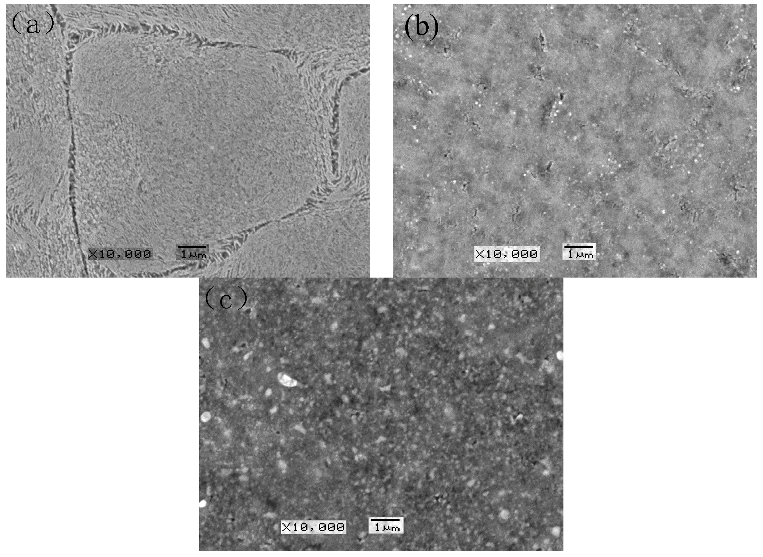
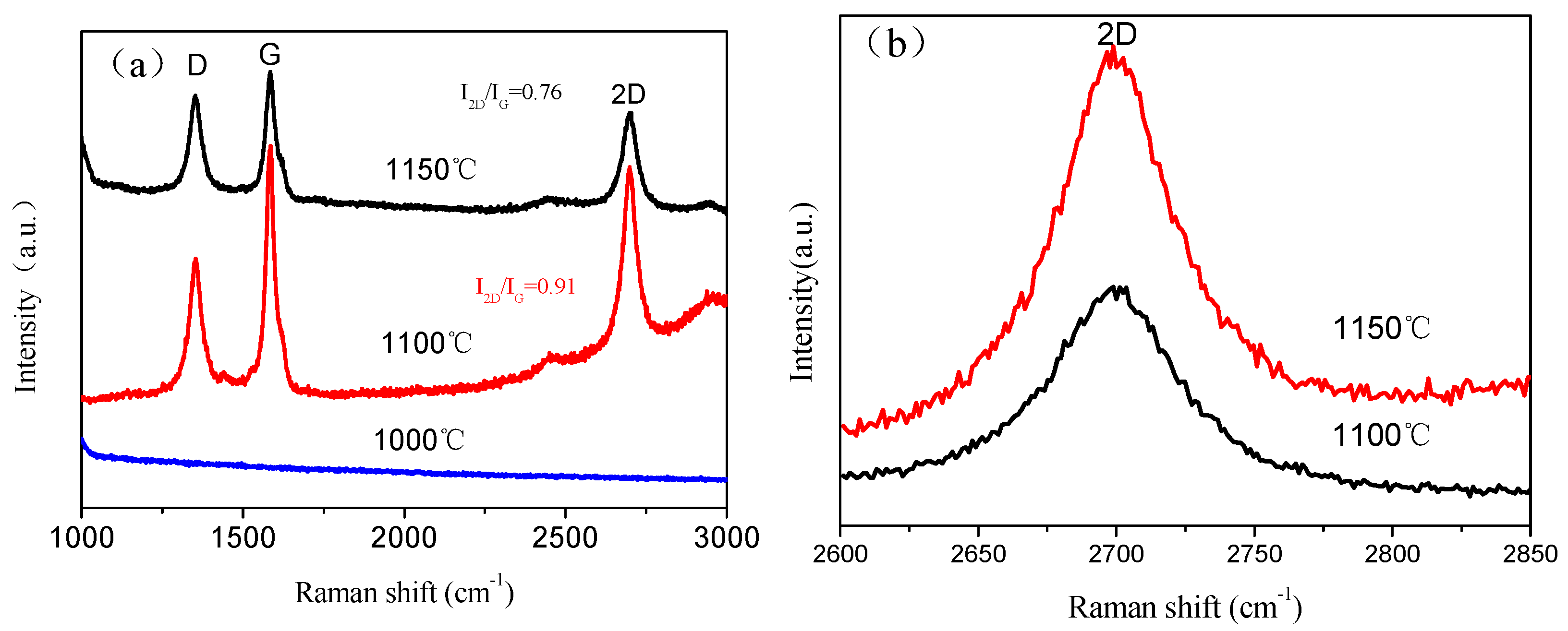
3.1. Surface Micromorphology

Figure 1 shows the morphology of Si substrates deposited in a CO atmosphere at different temperatures. It can be seen that when the preparation temperature was 1000 °C (Figure 1a), significant grain boundary defects appeared on the Si surface; the diameter of each grain was about 16.7 μm, and the surface was relatively rough. When the preparation temperature was 1100 °C (Figure 1b), the grain boundaries on the surface of the Si substrate completely disappeared, showing a cloud-like morphology with many pit-like defects, and the surface was uneven with undulations. When the preparation temperature reached 1150 °C (Figure 1c), the surface was similar to that of the sample prepared at 1100 °C/3 h (Figure 1b), the surface roughness continued to increase, and the grain boundaries were reduced. Moreover, defects (such as small pits, bumps, and so on) appeared on the film layer, as also shown in the Raman analysis results presented in the following part.

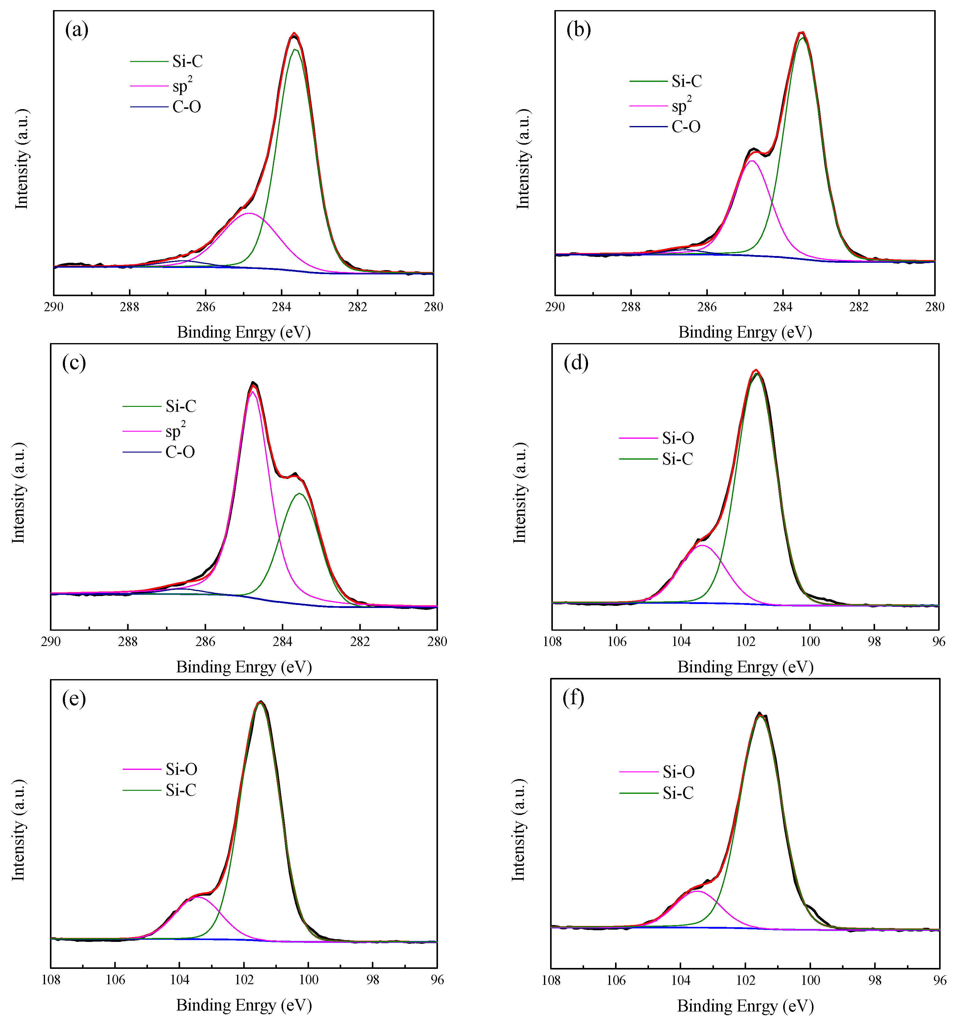
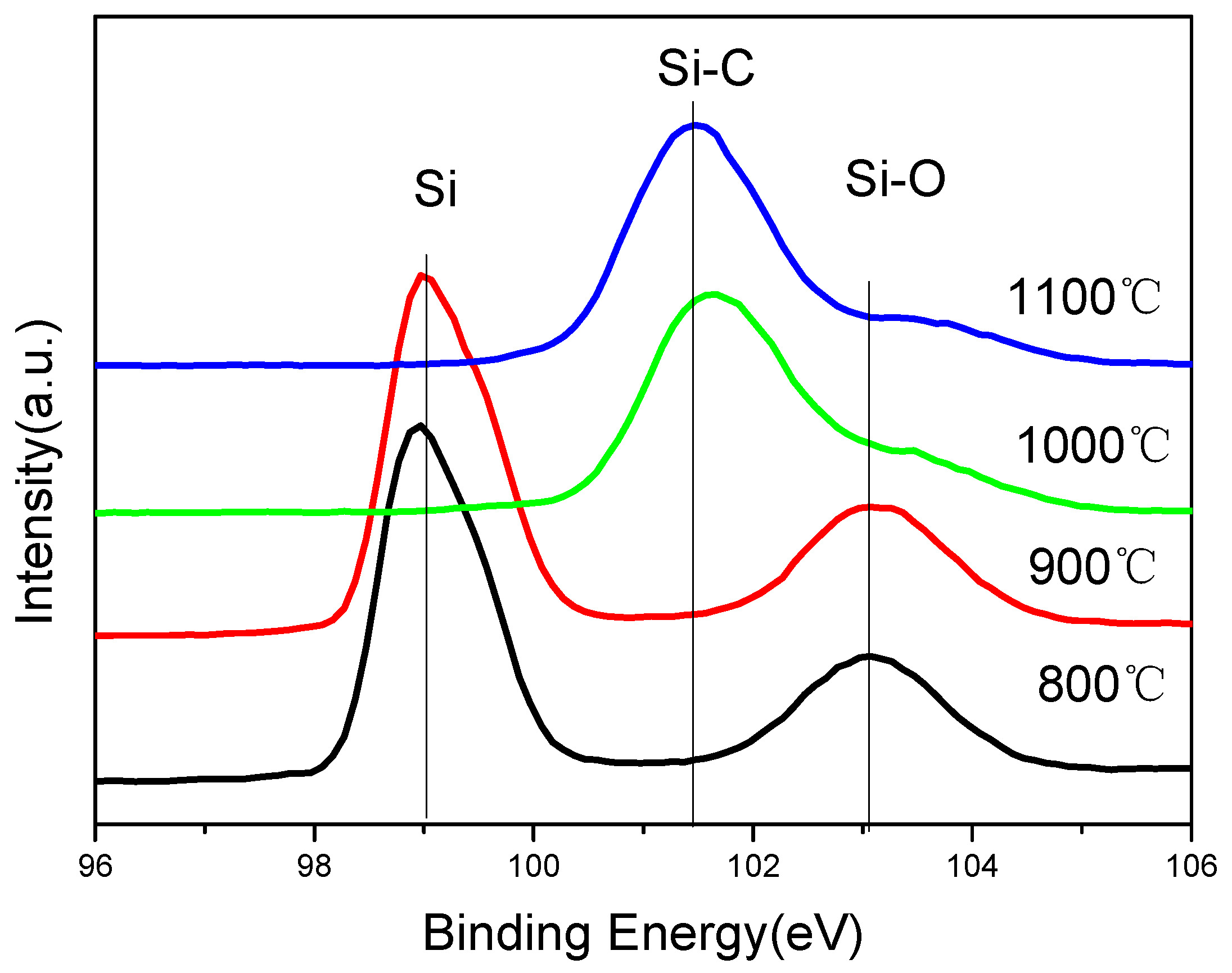
3.2. Surface Composition

XPS peak41 software (CUHK, Hongkong, China) (version 41) was used to fit the data of the Si substrate after deposition in a CO atmosphere at different temperatures; the results are shown in Figure 2. The elemental concentration of the graphene films is shown in Table 1. The error of the deconvolution process (X2) was controlled to within a value of 15, which shows that the fitting results are reliable. It can be seen from Figure 2 that the three elements (Si, C, and O) on the surface of the sample mainly existed in three forms: Si-C bonds (101 and 283.5 eV), Si-O bonds (103.5 eV), and sp2-C bonds (284.7 eV) [20,21]. Comparing and calculating the XPS results of the samples, it can be seen that the surface composition of the samples at 1000 °C/3 h was mainly 59.8% Si-C, 16.9% Si-O, and 23.3% sp2-C. When the reaction temperature was increased to 1100 °C/3 h, the Si-C content on the surface of the sample changed little (reducing to 56.3%), but the Si-O content dropped by 4.8% (reducing to 12.1%), while sp2-C increased to 36.1% (with an increase of 8.4%). When the reaction temperature was further increased to 1150 °C/3 h, the Si-C content and Si-O content on the surface of the sample decreased significantly, while the Si-C content decreased to 32.9% (with a decrease of about 41%), and the Si-O content decreased to 5.9% (with a decrease of about 51%). Finally, the content of sp2-C increased significantly to 61.2% (with an increase of 93%).
Figure 3a shows the results of a surface Raman spectroscopic analysis of the Si substrate after deposition in a CO atmosphere. It can be seen that there were no D, G, or 2D peaks in the Raman shift range of 1000–3000 cm−1 on the sample prepared at 1000 °C/3 h, indicating that the C content was too low at this time; this is consistent with the XPS results of C element (Figure 2a). When the reaction temperature increased to 1100 °C, a significant D peak (1350 cm−1), G peak (1580 cm−1), and 2D peak (2690 cm−1) appeared on the surface of the sample, indicating that a graphene film layer had formed. Further calculation showed that the 2D peak width of graphene was 50.79 cm−1 (see Figure 3b), and the I2D/IG was about 0.91. It could also be observed that the number of graphene layers on the Si surface was close to 2 [22,23]. When the reaction temperature increased to 1150 °C, significant graphene characteristic peaks (D peak, G peak, and 2D peak) remained, in which the graphene 2D peak width increased to 55.86 cm−1 (see Figure 3b) and the I2D/IG was reduced to 0.76. The calculation shows that there were three to five graphene layers.
Through our analyses of the microstructure and composition of graphene samples, it can be seen that with CO as the reactive carbon source, SiO2, SiC, and sp2-C were formed on the Si surface. When the temperature reached 1100 °C, sp2-C could exist in the form of graphene, indicating that a metal-free catalytic preparation of graphene on the Si surface had occurred [24]. However, when the temperature further increased to 1150 °C, the surface sp2-C content increased significantly because the reaction was too violent, increasing the defects in the graphene and reducing its quality.

3.3. Analysis of the Formation Mechanism

It can be seen that during the CVD reaction at 1100 °C/3 h, CO could react with the Si substrate at the interface, and finally, a Si/(SiC + SiO2)/Gr multilayer structure could form. Therefore, to study the formation mechanism of the multilayer structure, CVD treatments at 800 °C/1 min, 900 °C/1 min, 1000 °C/1 min, and 1100 °C/1 min were carried out in a CO atmosphere and a surface XPS analysis was performed (Figure 4). It can be seen that when the temperature was higher than 800 °C, the surface of the sample was mainly Si and SiO2, indicating that at this time, Si reacted with CO, forming SiO2 on the surface of the silicon wafer. However, the content of SiO2 was relatively small, and the XPS could still detect the matrix. When the temperature increased to 900 °C, the sample surface was still dominated by Si and SiO2, and the XPS diffraction peak characteristics were the same as those at 800 °C. In contrast, when the temperature reached 1000 °C, the characteristic peaks changed significantly: the Si peak disappeared, the SiO2 peak almost disappeared, and a prominent SiC diffraction peak appeared, which indicated that a (SiC + SiO2) layer was formed at this time. Additionally, the thickness of the layer was relatively high and the graphene completely covered the Si substrate. When the temperature continued to rise to 1100 °C, the characteristic peaks of SiC on the sample surface were sharper, the full width at half height was smaller, and the characteristic peaks of SiO2 could hardly be found. These results show that CO gas reacts with a Si substrate from 800 °C to form SiO2 first, followed by SiC, with SiC + SiO2 forming together on Si substrates [25,26].
Based on the above analysis and thermodynamic calculations, a reaction mechanism for preparing graphene films on silicon surfaces using CO as a carbon source is presented in Figure 5. At 800–900 °C, Si will react with O (the O generated by CO cracking) in CVD to form a SiO2 layer on its surface (Equation (1)) [25]. When the temperature increases to 1000 °C, the CO in the CVD will undergo a cracking reaction to generate [C] and CO2, and the newly generated [C] will react with the SiO2 on the surface to generate SiC (Equations (3) and (4)) [26,27]. In addition, [C] will diffuse into the interior through the mixed layer of SiO2 and SiC and continue to react with SiO2 and Si to generate SiC, increasing the thickness of the SiC and SiO2 layers (Equations (4) and (5)). On the other hand, the mixed layer of SiO2 and SiC generated on the surface creates conditions for [C] to aggregate, nucleate, diffuse, and grow, finally forming a uniform graphene layer. In addition, the CO2 produced in the CVD reaction during graphene growth will also etch the graphene film, inhibiting the accumulation of [C] in the direction perpendicular to the silicon wafer and promoting the growth of graphene in the plane direction, thereby reducing the number of graphene layers and improving the quality of the film layers [18].
Si + 2O2→SiO2
CO→[C] + O
2CO→[C] + CO2
SiO2 + C→SiC + CO2
Si + C→SiC

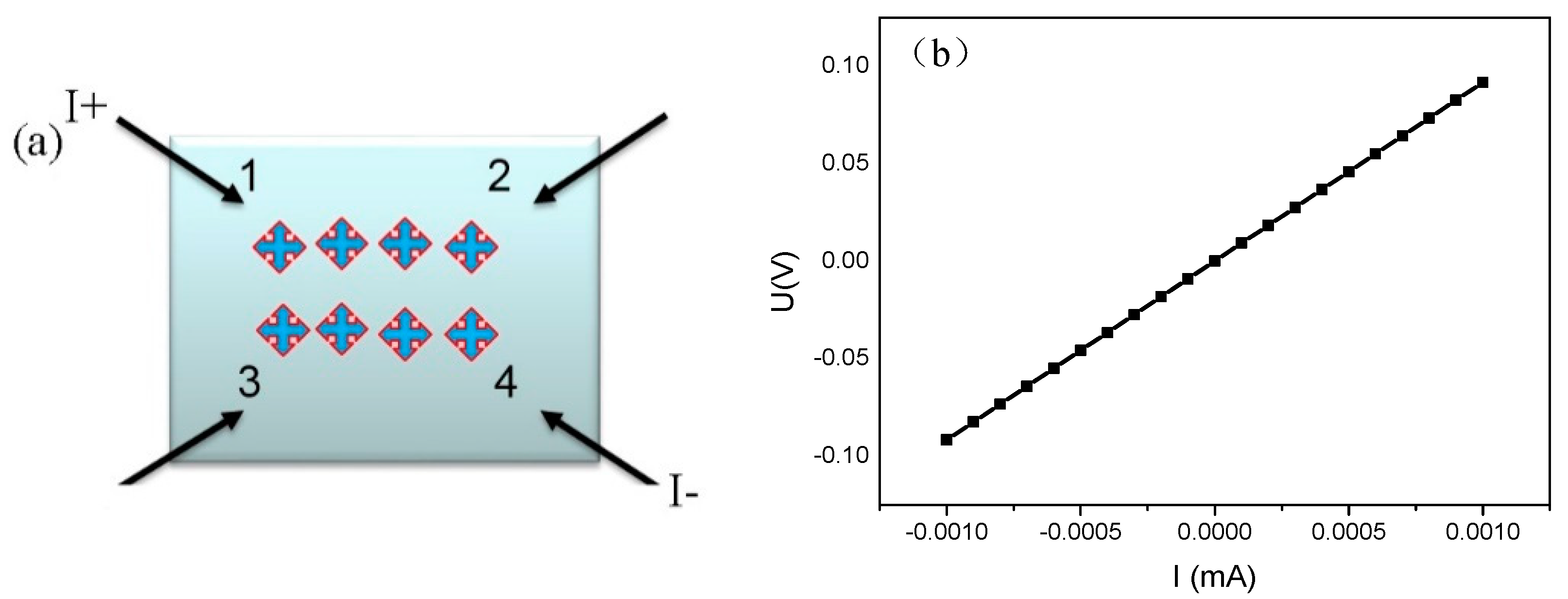
3.4. Electrical Properties of Graphene Films

The four-probe method was used to estimate graphene films’ resistivity and sheet resistance. During the measurements, four graphene electrodes measured the current between adjacent electrodes and the voltage between another pair of adjacent electrodes. As shown in Figure 6, when no magnetic field was applied, its volt–ampere characteristic curve was a straight line passing through the origin, indicating that the experimental electrode was in good ohmic contact with the graphene (Equation (6)) [28]:
ρ = π I n 2 U I d
where I is the current flowing through the film, U is the voltage generated by the current flowing through the film, and d is the thickness of the film, ln is mathematical function. Here, thickness d of the graphene was 1.7 nm (the number of graphene layers was ~5), and the resistivity of the film layer was calculated to be 7.06 × 10⁻⁷ Ω·m. Moreover, the experimentally measured sheet resistance of the graphene film was only 79 Ω/sq. Thus, it can be seen that using CO as a carbon source could avoid the hydrogen doping that occurs due to the presence of C-H gas in traditional graphene preparation methods. Furthermore, the content of the sp3 (C-H) structure in the arrangement of C atoms will not increase due to the locally formed point defects, improving the electrical properties of the graphene film [26,29]. The resistance value reached the same level as graphene prepared by metal catalysis (such as a copper foil surface) [30]. The performance was outstanding, and there was no need for subsequent peeling and transfer. This could enhance the commercial/applicability prospects of this approach.
A magnetic field was applied to the sample to measure the Hall effect of the graphene film. The applied magnetic field was 1.5 T. According to the Formula [19,31,32]:
R H = d B × U I
n = 1 R H × e
μ = 1 n e ρ
where B is is the strength of the magnetic field, e is electron charge (1.60 × 10⁻¹⁹ C) and d is the thickness of graphene. The Hall coefficient (RH) could be calculated as 1.04 × 10⁻⁷·m3·c−1, the carrier concentration (n) as 0.6 × 1026 m−3, and the carrier migration rate ( μ ) as 1473.1 cm2·V−1·S−1, respectively. In addition, since the size of the electrical performance test of the general graphene film was in the micron range, and the sample used in this experiment had the size of 5 mm × 5 mm, graphene defects were inevitably introduced during the tests. Therefore, the electrical performance of the film layer was slightly reduced.

4. Conclusions

In summary, catalyst-free direct growth of graphene on silicon wafer using a simple chemical vapor deposition method was demonstrated by SEM, Raman, and XPS characterizations. The graphene film layer was directly prepared on the surface of the silicon wafer under the condition of a metal-free catalyst with CO as the carbon source.
Above 800 °C, Si would react with O in a CVD tube furnace to form a SiO2 layer on the silicon wafer. When the temperature rose above 1000 °C, CO was decomposed into activated carbon atoms and CO2. The as-formed active carbon atoms would react with SiO2 to form SiC. The in situ generated SiC and SiO2 could promote the generation of activated carbon atoms, nucleate and grow on their surfaces, and connect to form a graphene film.
The number of graphene layers grown at 1100 °C was between two and three, while that at 1150 °C was between three and five. By increasing the temperature, the number of defects in the graphene increased. The electrical performance results showed that the obtained graphene film had a sheet resistance of 79 Ω/sq, a resistivity of 7.06 × 10⁻⁷ Ω·m, and a carrier migration rate of up to 1473.1 cm2 V−1·S−1.

Author Contributions

Data curation, F.H. and H.L.; Writing—review & editing, L.L., W.L. and Z.L.; Funding acquisition, Z.L. All authors have read and agreed to the published version of the manuscript.

Funding

This work was supported by Xi’an Postdoctoral Foundation and Sichuan Provincial Key Lab of Process Equipment and Control, Grant No. [GK202208].

Institutional Review Board Statement

Not applicable.

Informed Consent Statement

Not applicable.

Data Availability Statement

Not applicable.

Acknowledgments

This work was supported by Xi’an Postdoctoral Foundation and Sichuan Provincial Key Lab of Process Equipment and Control.

Conflicts of Interest

We declare that we have no economic or non-economic conflict of interest with any individual or organization in our work.

References

  1. Seo, J.; Lee, J.; Jang, A.; Choi, Y.; Kim, U.; Shin, H.; Park, H. Study of Cooling Rate on the Growth of Graphene via Chemical Vapor Deposition. Chem. Mater. 2017, 29, 4202–4208. [Google Scholar] [CrossRef]
  2. Wang, J.; Jin, X.; Li, C.; Wang, W.; Wu, H.; Guo, S. Graphene and graphene derivatives toughening polymers: Toward high toughness and strength. Chem. Eng. J. 2019, 370, 831–854. [Google Scholar] [CrossRef]
  3. Lin, H.C.; Jian, Q.F.; Bai, X.Y.; Li, D.Q.; Huang, Z.; Huang, W.T.; Feng, S.S.; Cheng, Z.G. Recent advances in thermal conductivity and thermal applications of graphene and its derivatives nanofluids. Appl. Therm. Eng. 2023, 218, 119176. [Google Scholar] [CrossRef]
  4. Ghosal, S.; Mondal, N.S.; Chowdhury, S.; Jana, D. Two novel phases of germa-graphene: Prediction, electronic and transport applications. Appl. Surf. Sci. 2023, 614, 156107. [Google Scholar] [CrossRef]
  5. Zhang, Y.; Xia, X.; Liu, B.; Deng, S.; Xie, D.; Liu, Q.; Wang, Y.; Wu, J.; Wang, X.; Tu, J. Multiscale Graphene-Based Materials for Applications in Sodium Ion Batteries. Adv. Energy Mater. 2019, 9, 1803342. [Google Scholar] [CrossRef]
  6. Pang, J.; Mendes, R.G.; Wrobel, P.S.; Wlodarski, M.D.; Ta, H.Q.; Zhao, L.; Giebeler, L.; Trzebicka, B.; Gemming, T.; Fu, L.; et al. Terminating Confinement Approach for Large-Area Uniform Monolayer Graphene Directly over Si/SiO\r, x\r, by Chemical Vapor Deposition. ACS Nano 2017, 11, 46–1956. [Google Scholar] [CrossRef] [PubMed]
  7. Wuttke, M.; Liu, Z.; Lu, H.; Narita, A.; Müllen, K. Direct Metal-Free Chemical Vapor Deposition of Graphene Films on Insulating Substrates for Micro-Supercapacitors with High Volumetric Capacitance. Batter. Supercaps 2019, 2, 929–933. [Google Scholar] [CrossRef] [Green Version]
  8. Tai, L.; Zhu, D.; Liu, X.; Yang, T.; Wang, L.; Wang, R.; Jiang, S.; Chen, Z.H.; Xu, Z.; Li, X. Direct Growth of Graphene on Silicon by Metal-Free Chemical Vapor Deposition. Nano-Micro. Lett. 2018, 10, 20. [Google Scholar] [CrossRef] [Green Version]
  9. Kruskopf, M.; Pierz, K.; Wundrack, S.; Stosch, R.; Dziomba, T.; Kalmbach, C.C.; Müller, A.; Baringhaus, J.; Tegenkamp, C.; Ahlers, F.J.; et al. Epitaxial Graphene on SiC: Modification of Structural and Electron Transport Properties by Substrate Pretreatment. J. Phys. Condens. Matter. 2015, 27, 185303. [Google Scholar] [CrossRef]
  10. Phong, N.; Behura, S.K.; Seacrist, M.R.; Berry, V. Intergrain Diffusion of Carbon Radical for Wafer-Scale, Direct Growth of Graphene on Si-Based Dielectrics. ACS Appl. Mater. Interfaces 2018, 10, 26517–26525. [Google Scholar] [CrossRef]
  11. Li, X.; Colombo, L.; Ruoff, R.S. Synthesis of Graphene Films on Copper Foils by Chemical Vapor Deposition. Adv. Mater. 2016, 28, 6264. [Google Scholar] [CrossRef] [PubMed]
  12. Lee, E.; Lee, S.G.; Lee, H.C.; Jo, M.; Yoo, M.S.; Cho, K. Direct Growth of Highly Stable Patterned Graphene on Dielectric Insulators using a Surface-Adhered Solid Carbon Source. Adv. Mater. 2018, 30, 1706569. [Google Scholar] [CrossRef] [PubMed]
  13. Ismach, A.; Druzgalski, C.; Penwell, S.; Zheng, M.; Javey, A.; Bokor, J.; Zhang, Y. Direct Chemical Vapor Deposition of Graphene on Dielectric Surfaces. Nano Lett. 2010, 10, 1542–1548. [Google Scholar] [CrossRef] [PubMed]
  14. Kim, H.H.; Chung, Y.; Lee, E.; Lee, S.K.; Cho, K. Water-free transfer method for CVD-grown graphene and its application to flexible air-stable graphene transistors. Adv. Mater. 2014, 26, 3213–3217. [Google Scholar] [CrossRef] [PubMed]
  15. Lee, W.H.; Park, J.; Sim, S.H.; Lim, S.; Cho, K. Surface-Directed Molecular Assembly of Pentacene on Monolayer Graphene for High-Performance Organic Transistors. J. Am. Chem. Soc. 2011, 133, 4447–4454. [Google Scholar] [CrossRef]
  16. Seekaew, Y.; Nantikan, T.; Adisorn, T.; Tanom, L.; Anurat, W.; Chatchawal, W. Conversion of Carbon Dioxide into Chemical Vapor Deposited Graphene with Controllable Number of Layers via Hydrogen Plasma Pre-Treatment. Membranes 2022, 12, 796. [Google Scholar] [CrossRef]
  17. Mu?Oz, R.; Munuera, C.; Martínez, J.I.; Azpeitia, J.; Gómez, A.; García, H. Low temperature metal free growth of graphene on insulating substrates by plasma assisted chemical vapor deposition. 2D Mater. 2016, 4, 015009. [Google Scholar] [CrossRef] [Green Version]
  18. Strudwick, A.J.; Weber, N.E.; Schwab, M.G.; Kettner, M.; Weitz, R.T.; Wünsch, J.R.; Müllen, K.; Sachdev, H. Chemical Vapor Deposition of High Quality Graphene Films from Carbon Dioxide Atmospheres. ACS Nano 2015, 9, 31–42. [Google Scholar] [CrossRef] [Green Version]
  19. Weber, N.E.; Binder, A.; Kettner, M.; Hirth, S.; Weitz, R.T.; Tomovi, Z. Metal-free synthesis of nanocrystalline graphene on insulating substrates by carbon dioxide-assisted chemical vapor deposition. Carbon 2017, 112, 201–207. [Google Scholar] [CrossRef]
  20. Zada, A.; Khan, M.; Hussain, Z.; Shah, M.I.A.; Ateeq, M.; Ullah, M.; Dang, A. Extended visible light driven photocatalytic hydrogen generation by electron induction from g-C3N4 nanosheets to ZnO through the proper heterojunction. Z. Für Phys. Chem. 2022, 236, 53–66. [Google Scholar] [CrossRef]
  21. Lv, C.; Cheng, H.; He, W.; Shah, M.I.A.; Xu, C.; Meng, X.; Jiao, L.; Wei, S.; Li, J.; Liu, L.; et al. Pd 3 cluster catalysis: Compelling evidence from in operando spectroscopic, kinetic, and density functional theory studies. Nano Res. 2016, 9, 2544–2550. [Google Scholar] [CrossRef]
  22. Liu, Q.F.; Gong, Y.P.; Wang, T.; Chan, W.L.; Wu, J. Metal-catalyst-free and controllable growth of high-quality monolayer and AB-stacked bilayer graphene on silicon dioxide. Carbon 2016, 96, 203–211. [Google Scholar] [CrossRef] [Green Version]
  23. Stankus, V.; Vasiliauskas, A.; Guobien, A.; Andruleviius, M.; Mekinis, A. Direct synthesis of graphene on silicon by reactive magnetron sputtering deposition. Surf. Coat. Technol. 2022, 437, 128361. [Google Scholar] [CrossRef]
  24. Yang, J.; Jiang, Q.; Chen, Z.; Hu, P.A.; Li, J.J.; Guo, C.Z.; Yu, G. Transfer-free synthesis of multilayer graphene on silicon nitride using reusable gallium catalyst. Diam. Relat. Mater. 2019, 91, 112–118. [Google Scholar] [CrossRef]
  25. Chen, J.; Wen, Y.; Guo, Y.; Wu, B.; Huang, L.P.; Xue, Y.Z.; Geng, D.C.; Wang, D.; Yu, G.; Liu, Y.Q. Oxygen-Aided Synthesis of Polycrystalline Graphene on Silicon Dioxide Substrates. J. Am. Chem. Soc. 2011, 133, 17548–17551. [Google Scholar] [CrossRef]
  26. Bremmer, G.M.; Zacharaki, E.; Sjåstad, A.O.; Navarro, V.; Frenken, J.W.; Kooyman, P.J. In situ TEM observation of the Boudouard reaction: Multi-layered graphene formation from CO on cobalt nanoparticles at atmospheric pressure. Faraday Discuss. 2017, 197, 337–351. [Google Scholar] [CrossRef] [Green Version]
  27. Chakrabarti, A.; Lu, J.; Skrabutenas, J.C.; Xu, T.; Xiao, Z.; Maguire, J.A.; Hosmane, N.S. Conversion of carbon dioxide to few-layer graphene. J. Mater. Chem. 2011, 21, 9491–9493. [Google Scholar] [CrossRef]
  28. Zhai, Z.; Shen, H.; Chen, J.; Li, X.; Jiang, Y. Evolution of structural and electrical properties of carbon films from amorphous carbon to nanocrystalline graphene on quartz glass by HFCVD. ACS Appl. Mater. Interfaces 2018, 10, 17427–17436. [Google Scholar] [CrossRef]
  29. Losurdo, M.; Giangregorio, M.M.; Capezzuto, P.; Bruno, G. Graphene CVD growth on copper and nickel: Role of hydrogen in kinetics and structure. Phys. Chem. Chem. Phys. 2011, 13, 20836–20843. [Google Scholar] [CrossRef]
  30. Elias, D.C.; Nair, R.R.; Mohiuddin, T.M.G.; Morozov, S.V.; Blake, P.; Halsall, M.P.; Ferrari, A.C.; Boukhvalov, D.W.; Katsnelson, M.I.; Geim, A.K. Control of graphene’s properties by reversible hydrogenation: Evidence for graphane. Science 2009, 323, 610–613. [Google Scholar] [CrossRef] [Green Version]
  31. Kim, H.; Lee, Y.; Bae, S. Roll-to-roll production of 30-inch graphene films for transparent electrodes. Nat. Nanotechnol. 2010, 5, 574–578. [Google Scholar] [CrossRef] [Green Version]
  32. Li, X.; Zhu, Y.; Cai, W.; Han, B.; Chen, D.; Piner, R.D.; Colombo, L.; Ruoff, R.S. Transfer of Large-Area Graphene Films for High-Performance Transparent Conductive Electrodes. Nano Lett. 2009, 9, 4359–4363. [Google Scholar] [CrossRef] [PubMed]
Figure 1. SEM images of the Gr surface topographies (a) 1000 °C, (b) 1100 °C, (c) 1150 °C.
Coatings 13 01052 g001
Figure 2. XPS spectra fitting of Si peak and C peak (a) 1000 °C—C peak, (b) 1100 °C—C peak, (c) 1150 °C—C peak, (d) 1000 °C—Si peak, (e) 1100 °C—Si peak, (f) 1150 °C—Si peak.
Coatings 13 01052 g002
Figure 3. Raman spectra of Gr films at different heat treatment temperatures (a) and 2D peak intensity (b).
Coatings 13 01052 g003
Figure 4. XPS spectra of specimen surfaces with different preparation temperatures.
Coatings 13 01052 g004
Figure 5. Mechanism of Gr formation on Si surface at 1100 °C by CVD.
Coatings 13 01052 g005
Figure 6. Electrical performance testing of Gr on Si surface (a) electrical performance test diagram, (b) voltammetry curve.
Coatings 13 01052 g006
Table 1. Elemental analysis of XPS.
Sample (Temperature)Si-C (at%)Si-O (at%)sp2-C (at%)X2
Binding Energy (eV)283.5103.5284.7
1000 °C59.816.923.33.31
1100 °C56.812.136.17.02
1150 °C32.95.961.214.43
Disclaimer/Publisher’s Note: The statements, opinions and data contained in all publications are solely those of the individual author(s) and contributor(s) and not of MDPI and/or the editor(s). MDPI and/or the editor(s) disclaim responsibility for any injury to people or property resulting from any ideas, methods, instructions or products referred to in the content.

