
Effect of the Working Pressure and Oxygen Gas Flow Rate on the Fabrication of Single-Phase Ag2O Thin Films


Abstract
:1. Introduction
2. Experimental Section
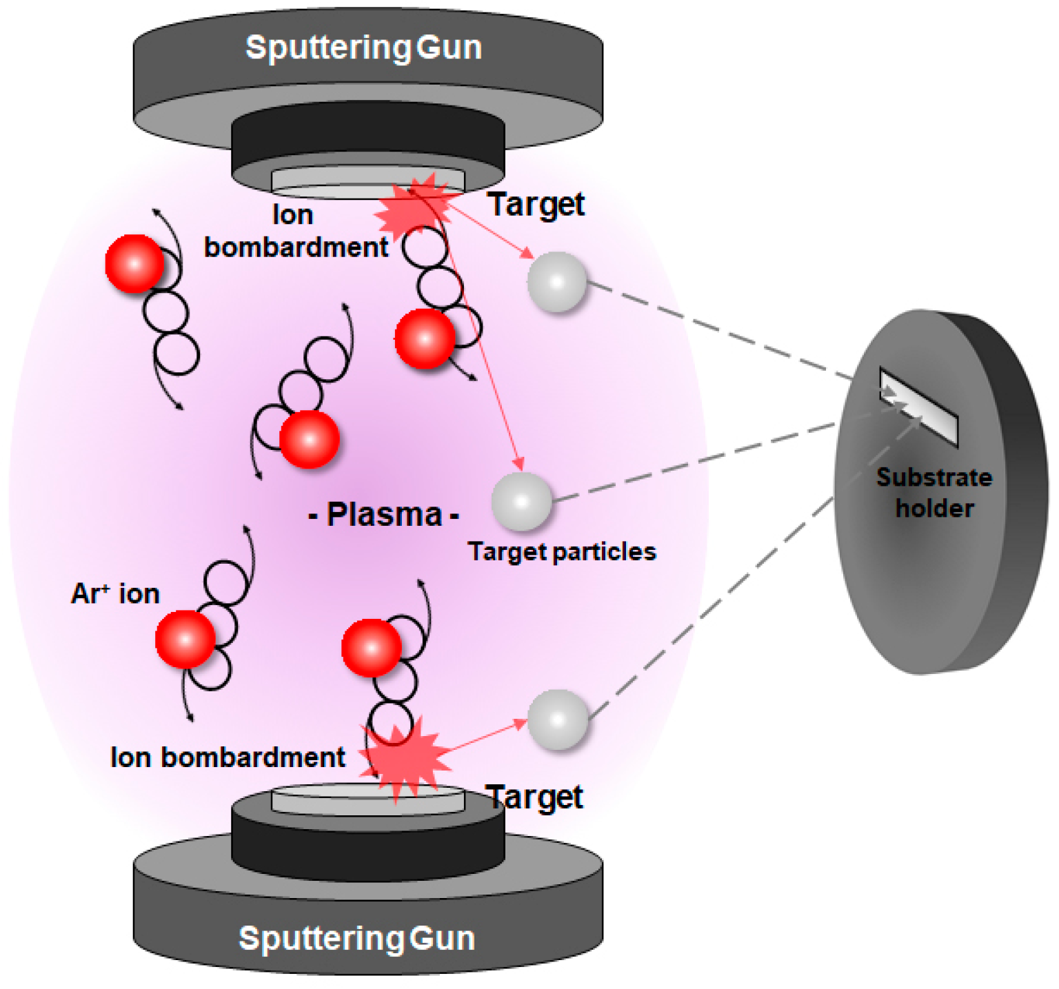
2.1. Fabrication
2.2. Evaluation of Samples
3. Results and Discussion
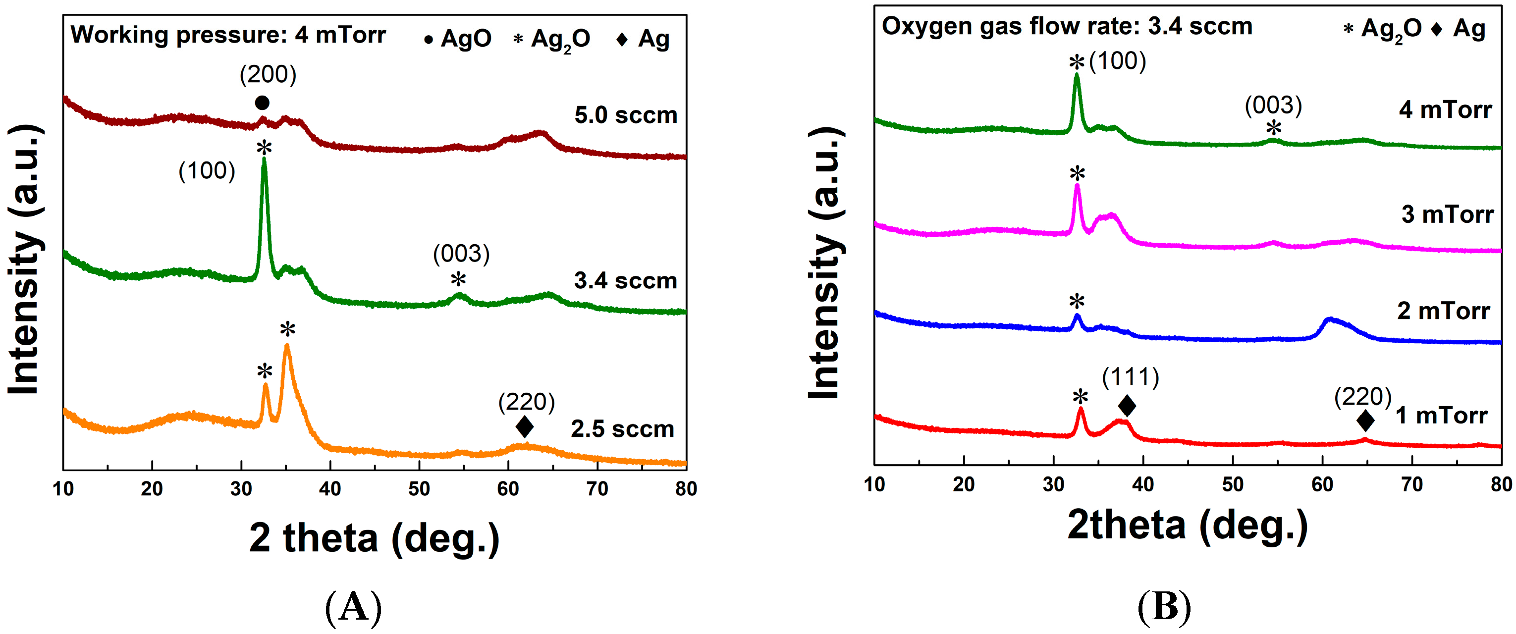
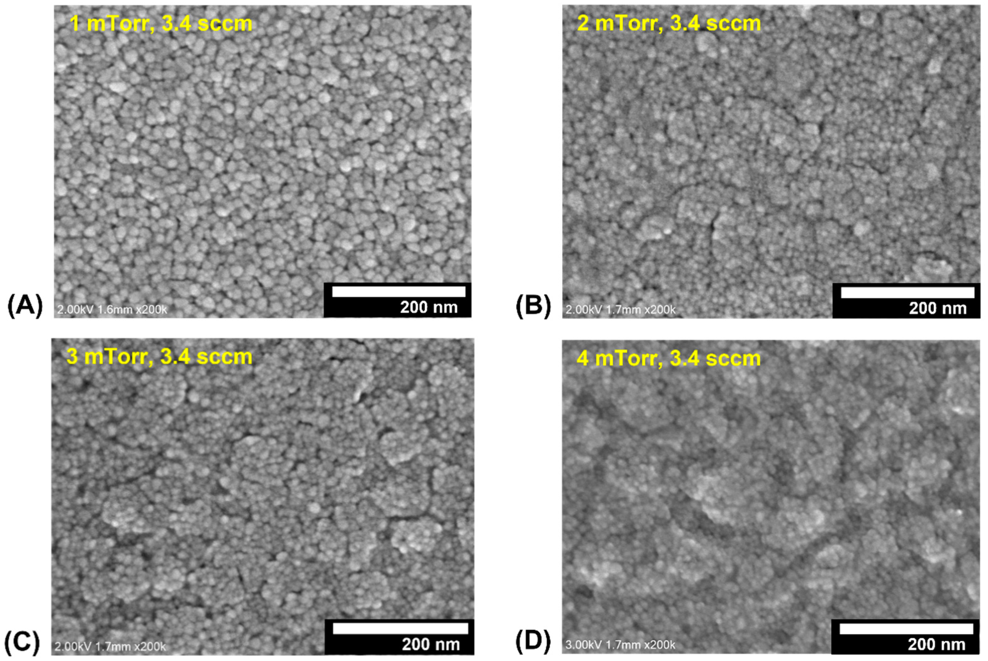
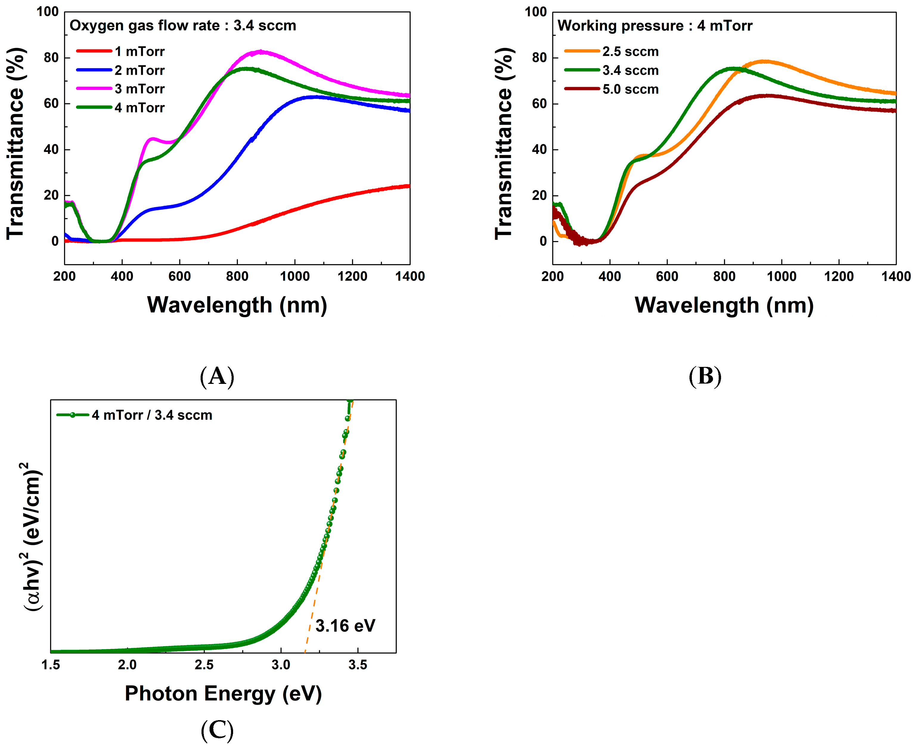
3.1. Evaluation of Ag2O Thin Films
3.2. Evaluation of Ag2O Thin Films Post-Annealed at RT to 400 °C
4. Conclusions
Author Contributions
Funding
Institutional Review Board Statement
Informed Consent Statement
Data Availability Statement
Conflicts of Interest
References
- Park, T.; Park, S.; Min, J.; Jung, Y.; Kyoung, S.; Kang, T.; Kim, K.; Rim, Y.; Hong, J. Temperature-Dependent Self-Powered Solar-Blind Photodetector Based on Ag2O/β-Ga2O3 Heterojunction. Nanomaterials 2022, 12, 2983. [Google Scholar] [CrossRef] [PubMed]
- Liang, Y.; Hsu, Y. Design of thin-film configuration of SnO2–Ag2O composites for NO2 gas-sensing applications. Nanotechnol. Rev. 2022, 11, 1842–1853. [Google Scholar] [CrossRef]
- Kumar, K.; Yadav, R.; Devi, S.; Singh, P.; Husale, S.; Tyagi, S.; Kaur, D. Effective ways to enhance the performance of n-MoS2/p-CuO heterojunction based self-powered photodetectors. Sol. Energy Mater. Sol. Cells 2023, 255, 112285. [Google Scholar] [CrossRef]
- Debnath, R.; Xie, T.; Wen, B.; Li, W.; Ha, J.Y.; Sullivan, N.F.; Nguyen, N.V.; Motayed, A. A solution-processed high-efficiency p-NiO/n-ZnO heterojunction photodetector. Rsc Adv. 2015, 5, 14646–14652. [Google Scholar] [CrossRef]
- Nwanya, A.C.; Ugwuoke, P.E.; Ezekoye, B.A.; Osuji, R.U.; Ezema, F.I. Structural and optical properties of chemical bath deposited silver oxide thin films: Role of deposition time. Adv. Mater. Sci. Eng. 2013, 2013, 450820. [Google Scholar] [CrossRef] [Green Version]
- Korkmaz, N.; Karadağ, A. Microwave assisted green synthesis of Ag, Ag2O, and Ag2O3 nanoparticles. J. Turk. Chem. Soc. Sect. A Chem. 2021, 8, 585–592. [Google Scholar] [CrossRef]
- Laskri, A.; Drici, A.; Boulouma, A.; Amara, A.; Bernede, J.C. Investigation of microstructural and optical properties of Ag3O4 thin films sprayed onto glass substrate. J. Nano Res. 2019, 58, 90–101. [Google Scholar] [CrossRef]
- Salim, E.T.; Awayiz, M.T.; Mahdi, R.O. Tea concentration effect on the optical, structural, and surface roughness of Ag2O thin films. Dig. J. Nanomater. Biostruct. 2019, 14, 1151–1159. [Google Scholar]
- Pierson, J.F.; Rousselot, C. Stability of reactively sputtered silver oxide films. Surf. Coat. Technol. 2005, 200, 276–279. [Google Scholar] [CrossRef]
- Fortin, E.; Weichman, F.L. photoconductivity in Ag2O. Phys. Status Solidi (B) 1964, 5, 515–519. [Google Scholar] [CrossRef]
- Barik, U.K.; Srinivasan, S.; Nagendra, C.L.; Subrahmanyam, A. Electrical and optical properties of reactive DC magnetron sputtered silver oxide thin films: Role of oxygen. Thin Solid Film. 2003, 429, 129–134. [Google Scholar] [CrossRef]
- Jamal, R.K.; Mutlak, F.A.; Ibrahim, F.T.; Nayef, U.M. Synthesis of Ag2O films by pulsed laser deposited on porous silicon as gas sensor application. Optik 2020, 218, 164971. [Google Scholar] [CrossRef]
- Wang, X.; Li, S.; Yu, H.; Yu, J.; Liu, S. Ag2O as a new visible-light photocatalyst: Self-stability and high photocatalytic activity. Chem. A Eur. J. 2011, 17, 7777–7780. [Google Scholar] [CrossRef]
- Fang, F.; Li, Q.; Shang, J.K. Enhanced visible-light absorption from Ag2O nanoparticles in nitrogen-doped TiO2 thin films. Surf. Coat. Technol. 2011, 205, 2919–2923. [Google Scholar] [CrossRef]
- Satyanarayana, N.; Xie, X.; Rambabu, B. Sol–gel synthesis and characterization of the Ag2O–SiO2 system. Mater. Sci. Eng. B 2000, 72, 7–12. [Google Scholar] [CrossRef]
- Narayana Reddy, P.; Sreedhar, A.; Hari Prasad Reddy, M.; Uthanna, S.; Pierson, J.F. The effect of oxygen partial pressure on physical properties of nano-crystalline silver oxide thin films deposited by RF magnetron sputtering. Cryst. Res. Technol. 2011, 46, 961–966. [Google Scholar] [CrossRef]
- Saroja, G.; Vasu, V.; Nagarani, N. Optical Studies of Ag2O thin film prepared by electron beam evaporation method. Open J. Met. 2013, 3, 57–63. [Google Scholar] [CrossRef] [Green Version]
- Entezar Mehdi, H.; Hantehzadeh, M.R.; Valedbagi, S. Physical properties of silver oxide thin film prepared by DC magnetron sputtering: Effect of oxygen partial pressure during growth. J. Fusion Energy 2013, 32, 28–33. [Google Scholar] [CrossRef]
- Lee, M.; Park, Y.; Kim, K.; Hong, J. Influence of sputtering conditions on the properties of aluminum-doped zinc oxide thin film fabricated using a facing target sputtering system. Thin Solid Film. 2020, 703, 137980. [Google Scholar] [CrossRef]
- Hong, J.; Jang, K.; Park, Y.; Choi, H.; Kim, K. Preparation of ZnO based thin films for OLED anode by facing targets sputtering system. Mol. Cryst. Liq. Cryst. 2011, 538, 103–111. [Google Scholar] [CrossRef]
- Park, S.; Yoon, Y.; Lee, S.; Park, T.; Kim, K.; Hong, J. Thermoinduced and Photoinduced Sustainable Hydrophilic Surface of Sputtered-TiO2 Thin Film. Coatings 2021, 11, 1360. [Google Scholar] [CrossRef]
- Hong, J.; Matsushita, N.; Kim, K.H. Investigation of the effect of oxygen gas on properties of GAZO thin films fabricated by facing targets sputtering system. Semicond. Sci. Technol. 2014, 29, 075007. [Google Scholar] [CrossRef]
- Araújo, A.; Mendes, M.J.; Mateus, T.; Vicente, A.; Nunes, D.; Calmeiro, T.; Fortunato, E.; Aguas, H.; Martins, R. Influence of the substrate on the morphology of self-assembled silver nanoparticles by rapid thermal annealing. J. Phys. Chem. C 2016, 120, 18235–18242. [Google Scholar] [CrossRef]
- Mirzaeian, M.; Ogwu, A.A.; Jirandehi, H.F.; Aidarova, S.; Ospanova, Z.; Tsendzughul, N. Surface characteristics of silver oxide thin film electrodes for supercapacitor applications. Colloids Surf. A Physicochem. Eng. Asp. 2017, 519, 223–230. [Google Scholar] [CrossRef] [Green Version]
- Fatimah, S.; Ragadhita, R.; Al Husaeni, D.F.; Nandiyanto, A.B.D. How to calculate crystallite size from x-ray diffraction (XRD) using Scherrer method. ASEAN J. Sci. Eng. 2022, 2, 65–76. [Google Scholar] [CrossRef]
- Yang, J.L.; Lai, Y.S.; Chen, J.S. Effect of heat treatment on the properties of non-stoichiometric p-type nickel oxide films deposited by reactive sputtering. Thin Solid Film. 2005, 488, 242–246. [Google Scholar] [CrossRef]
- Hanaor, D.A.H.; Triani, G.; Sorrell, C.C. Morphology and photocatalytic activity of highly oriented mixed phase titanium dioxide thin films. Surf. Coat. Technol. 2011, 205, 3658–3664. [Google Scholar] [CrossRef] [Green Version]
- Hong, J.; Katsumata, K.-i.; Matsushita, N. Fabrication of Al-Doped ZnO Film with High Conductivity Induced by Photocatalytic Activity. J. Electron. Mater. 2016, 45, 4875–4880. [Google Scholar] [CrossRef]
- Coulter, J.B.; Birnie, D.P. Assessing Tauc Plot Slope Quantification: ZnO Thin Films as a Model System. Phys. Status Solidi Basic Res. 2018, 255, 1700393. [Google Scholar] [CrossRef]
- Park, S.; Park, T.; Park, J.H.; Min, J.Y.; Jung, Y.; Kyoung, S.; Kang, T.Y.; Kim, K.H.; Rim, Y.S.; Hong, J. Ag2O/β-Ga2O3 Heterojunction-Based Self-Powered Solar Blind Photodetector with High Responsivity and Stability. ACS Appl. Mater. Interfaces 2022, 14, 25648–25658. [Google Scholar] [CrossRef]
- Tsendzughul, N.T.; Ogwu, A.A. Physicochemical Aspects of the Mechanisms of Rapid Antimicrobial Contact-Killing by Sputtered Silver Oxide Thin Films under Visible Light. ACS Omega 2019, 4, 16847–16859. [Google Scholar]
- Firet, N.J.; Blommaert, M.A.; Burdyny, T.; Venugopal, A.; Bohra, D.; Longo, A.; Smith, W.A. Operando EXAFS study reveals presence of oxygen in oxide-derived silver catalysts for electrochemical CO2 reduction. J. Mater. Chem. A 2019, 7, 2597–2607. [Google Scholar] [CrossRef] [Green Version]
- Pinto, G.; Dante, S.; Rotondi, S.M.C.; Canepa, P.; Cavalleri, O.; Canepa, M. Spectroscopic Ellipsometry Investigation of a Sensing Functional Interface: DNA SAMs Hybridization. Adv. Mater. Interfaces 2022, 9, 2200364. [Google Scholar] [CrossRef]
- Gao, C.; Huang, J.; Li, H.; Sun, K.; Lai, Y.; Jia, M.; Jiang, L.; Liu, F. Fabrication of Sb2S3 thin films by sputtering and post-annealing for solar cells. Ceram. Int. 2019, 45, 3044–3051. [Google Scholar] [CrossRef]
- Fang, Z.B.; Yan, Z.J.; Tan, Y.S.; Liu, X.Q.; Wang, Y.Y. Influence of post-annealing treatment on the structure properties of ZnO films. Appl. Surf. Sci. 2005, 241, 303–308. [Google Scholar] [CrossRef]
- Gao, X.Y.; Wang, S.Y.; Li, J.; Zheng, Y.X.; Zhang, R.J.; Zhou, P.; Chen, L.Y. Study of structure and optical properties of silver oxide films by ellipsometry, XRD and XPS methods. Thin Solid Film. 2004, 455, 438–442. [Google Scholar] [CrossRef]


| Parameters | Conditions |
|---|---|
| Thickness | 150 nm |
| Targets | Ag (99.99%), 4″ |
| Substrate | Soda–lime glass |
| Input power | 50 W |
| Working pressure | 1, 2, 3, and 4 mTorr |
| Gas flow rate | O2: 2.5, 3.4, and 5 sccm; Ar: 10 sccm |
| O2 Gas Flow Rate (sccm) | Lattice Constant (Å) | Crystallite Size (nm) |
|---|---|---|
| 2.5 | 4.65 | 8.63 |
| 3.4 | 4.67 | 11.25 |
| 5.0 | 4.77 | 15.68 |
| Working Pressure (mTorr) | Lattice Constant (Å) | Crystallite Size (nm) |
|---|---|---|
| 1 | 4.71 | 12.77 |
| 2 | 4.66 | 12.13 |
| 3 | 4.66 | 12.49 |
| 4 | 4.67 | 11.25 |
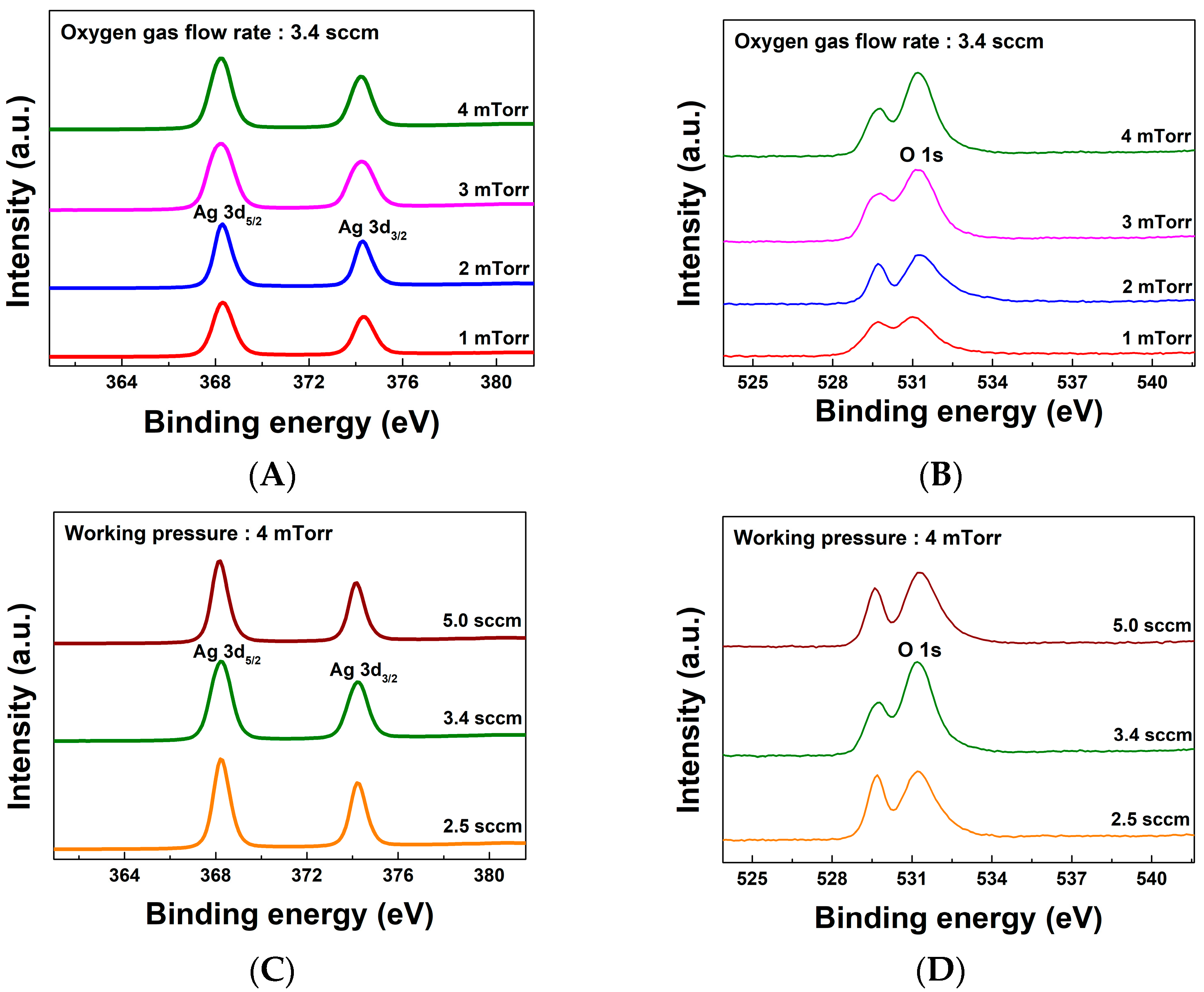
| Sample Identifier | Ag 3d% | O 1s% | Oxygen Versus Silver |
|---|---|---|---|
| 1 mTorr, 3.4 sccm | 28.30 | 16.03 | 1.77 |
| 2 mTorr, 3.4 sccm | 25.05 | 16.41 | 1.53 |
| 3 mTorr, 3.4 sccm | 33.67 | 22.08 | 1.52 |
| 4 mTorr, 2.5 sccm | 31.92 | 20.29 | 1.57 |
| 4 mTorr, 3.4 sccm | 33.55 | 23.80 | 1.50 |
| 4 mTorr, 5.0 sccm | 26.98 | 19.30 | 1.40 |
Disclaimer/Publisher’s Note: The statements, opinions and data contained in all publications are solely those of the individual author(s) and contributor(s) and not of MDPI and/or the editor(s). MDPI and/or the editor(s) disclaim responsibility for any injury to people or property resulting from any ideas, methods, instructions or products referred to in the content. |
© 2023 by the authors. Licensee MDPI, Basel, Switzerland. This article is an open access article distributed under the terms and conditions of the Creative Commons Attribution (CC BY) license (https://creativecommons.org/licenses/by/4.0/).
Share and Cite
Choi, J.; Seong, J.; Park, S.; Kim, H.; Kim, S.; Kim, K.H.; Hong, J. Effect of the Working Pressure and Oxygen Gas Flow Rate on the Fabrication of Single-Phase Ag2O Thin Films. Coatings 2023, 13, 1061. https://doi.org/10.3390/coatings13061061
Choi J, Seong J, Park S, Kim H, Kim S, Kim KH, Hong J. Effect of the Working Pressure and Oxygen Gas Flow Rate on the Fabrication of Single-Phase Ag2O Thin Films. Coatings. 2023; 13(6):1061. https://doi.org/10.3390/coatings13061061
Chicago/Turabian StyleChoi, Jiyoon, Jiha Seong, Sangbin Park, Hyungmin Kim, Sangmo Kim, Kyung Hwan Kim, and Jeongsoo Hong. 2023. "Effect of the Working Pressure and Oxygen Gas Flow Rate on the Fabrication of Single-Phase Ag2O Thin Films" Coatings 13, no. 6: 1061. https://doi.org/10.3390/coatings13061061
APA StyleChoi, J., Seong, J., Park, S., Kim, H., Kim, S., Kim, K. H., & Hong, J. (2023). Effect of the Working Pressure and Oxygen Gas Flow Rate on the Fabrication of Single-Phase Ag2O Thin Films. Coatings, 13(6), 1061. https://doi.org/10.3390/coatings13061061