
Photoconductive Response to Pulsed UV Light of CsPbCl3 Flexible Thin Films Grown by Magnetron Sputtering
by
 , , , and
Mara Bruzzi
1,2,3,* ,
,
Naomi Falsini
4,
Nicola Calisi
3,5,
Paolo Scardi
6 and
Anna Vinattieri
1,2,3,7 1
Dipartimento di Fisica e Astronomia, Università Degli Studi di Firenze, 50019 Florence, Italy
2
Istituto Nazionale di Fisica Nucleare—INFN, Sezione di Firenze, 50019 Florence, Italy
3
INSTM, Consorzio Interuniversitario Nazionale per la Scienza e Tecnologia dei Materiali, 50121 Florence, Italy
4
ENEA, Italian National Agency for New Technologies, Energy and Sustainable Economic Development, Fusion and Technology for Nuclear Safety and Security Department, Nuclear Safety, Security and Sustainability Division, 40129 Bologna, Italy
5
Dipartimento di Ingegneria Industriale, University of Florence, 50139 Florence, Italy
6
Dipartimento di Ingegneria Civile, Ambientale e Meccanica, Università di Trento, 38123 Trento, Italy
7
European Laboratory for Non-linear Spectroscopy (LENS), University of Florence, 50019 Florence, Italy
*
Author to whom correspondence should be addressed.
Coatings 2023, 13(6), 1128; https://doi.org/10.3390/coatings13061128
Submission received: 30 April 2023
/
Revised: 7 June 2023
/
Accepted: 13 June 2023
/
Published: 20 June 2023
(This article belongs to the Special Issue Optical and Electrical Properties and Applications of Semiconductors)
Abstract
:CsPbCl3 perovskite is attracting increasing interest in ultraviolet (UV) detection due to its optical band gap and superior intrinsic optoelectronic properties. In this study, a novel one-step magnetron sputtering technique was applied for fabricating CsPbCl3 polycrystalline films on flexible plastic substrates with interdigitated contacts. The photoconductive response of 500 nm and 1 µm thick films to pulsed ultraviolet (UV) light in the 0.1–100 Hz frequency range and intensity of 10–500 W/m2 was tested at room temperature. The experimental results demonstrated the good performances of the CsPbCl3 films in terms of signal stability, fast response to transient signal, detectivity, light dynamic range, and dark current noise for the photodetection of pulsed UV light.
1. Introduction
UV photodetectors for commercial applications should exhibit high UV responsivity, solar blindness, a linear dependence of the photocurrent on optical power, room-temperature operation, and facile and low-cost fabrication methods [1]. UV photodetectors are generally based on conventional wide-band-gap semiconductors, such as ZnO, GaN, and ZnMgO, which have limitations such as high-temperature treatments and low carrier mobilities [1,2,3,4]. Novel materials for next-generation UV photodetectors, such as inorganic perovskites, are being studied due to their low production costs and high optoelectronic performances [5,6]. Among these materials, CsPbCl3, is characterized by superior optoelectronic properties, a wide band gap, and a high exciton binding energy, which make it a promising candidate for UV photodetection [7,8,9,10]. Most CsPbCl3 photodetectors studied in the recent past have employed CsPbCl3 nanocrystals, while studies on CsPbCl3 polycrystalline films have been limited due to the difficult precursor solubility, which makes solution-based deposition methods, which are commonly employed for the fabrication of perovskite films, impractical. Recently, a novel one-step deposition technique, Radio Frequency (RF) magnetron sputtering, has been demonstrated to fabricate CsPbCl3 polycrystalline thin films with good optoelectronic and morphological properties [11,12]. Magnetron sputtering offers several advantages over conventional synthesis methods. As a physical vapor deposition (PVD) technique, it eliminates the need for solvents, which can damage the substrate, making it safer and more environmentally friendly. Furthermore, magnetron sputtering does not require high temperatures, and it allows for deposition on virtually all substrate types. Finally, our one-step process utilizes a single target, simplifying the process and facilitating scale-up.
In the past decade, pulsed ultraviolet (UV) light technology has emerged as a non-chemical and non-ionizing approach to decontaminate food products and for general disinfection purposes [13,14,15]. Pulsed UV-light technology offers effective inactivation of pathogens within a significantly shorter period of time compared to other technologies. It provides a viable alternative to ionizing irradiation processes, allowing to operate without the involvement of chemicals or chemical residues. In these specific applications, high energy pulses are delivered with typical frequencies of 0.1–100 Hz, an energy density of a few J/cm2, and pulse durations ranging from fraction of seconds to a few tens of seconds throughout the total duration of the treatment [13,14,15]. Low-cost, flexible UV photodetectors are appealing due to their easy conformation to various surfaces and environments, enabling the sensing of pulsed UV light during decontamination processes.
In this work, we conducted the first photoconductivity studies on CsPbCl3 thin films deposited on plastic flexible substrates using the RF magnetron sputtering technique. The aim was to verify their possible application for the photodetection and monitoring of pulsed UV light. Experimental tests were performed using pulsed UV light in the frequency range of 0.1–100 Hz and intensities ranging from 10–500 W/m2.
2. Materials and Methods
Cesium lead chloride (CsPbCl3) films were deposited at room temperature using a 13.56 MHz Radio Frequency (RF) Korvus HEX (Korvus Technology Ltd., London, UK) magnetron sputtering system [10,15,16] on soda–lime glass substrates and PET substrates equipped with an array of palladium interdigitated electrodes spaced 100 μm apart. The CsCl and PbCl2 precursor salts, in equal molar ratio, were ground using a mixer mill (Retsch model MM400) to produce the perovskite powder following the method described in [17]. The sputtering target was a 5 cm diameter disk manufactured by pressing the perovskite powder with a pneumatic press (11.5 MPa working pressure) for 24 h at 150 °C. The sputtering deposition was carried out at room temperature with a 20 W RF power and a 20 sccm Ar gas flow, maintaining a dynamic working pressure of 0.2 Pa. The deposition rates ranged from 5–7 × 10⁻² nm/s. The target distance was approximately 15 cm, and deposition times were approximately 2–3 h. The film thickness was monitored using a quartz crystal microbalance in the sputtering chamber, and rotation of the sample holder ensured thickness uniformity across the substrate.
The samples were characterized using scanning electron microscopy (SEM), X-ray photoelectron spectroscopy (XPS), and X-ray diffraction (XRD) to assess morphology and stoichiometry. Scanning electron microscopy was performed with a Philips XL30 SFEG SEM 30 KV electron microscope (Philips S.p.A., Milan, Italy). XPS measurements were carried our using a setup equipped with an X-ray source (VSW Scientific Instrument Limited model TA10, Mg Kα radiation, 1253.6 eV NorthHampton, UK) and a hemispherical analyzer (VSW Scientific Instrument Limited model HA100) with a 16-channel detector. XRD spectra were collected using an X’Pert diffractometer (Panalytical, Malvern, UK) equipped with a CoKα X-ray source (40 kV, 40 mA), a polycapillary optics in the primary beam (with 1 mm in equatorial direction and 10 mm height, beam divergence 0.3°), and a flat graphite crystal analyzer in the secondary beam, positioned before the proportional counter. The experiments were performed in grazing incidence (angle 0.9°) and a θ/2θ configuration. Phase identification was based on the ICDD PDF-4+ database, XRD card #18-0366, for the tetragonal phase of CsPbCl3, Space Group P4mm (99), with unit cell parameters of a = b = 5.584 A° and c = 5.623 A°.
Transmittance spectra were measured at room temperature using a broadband lamp (Thorlabs SLS201L Thorlabs Inc., Sparta Ave Newton, NJ, USA) and a monochromator (Acton SpectraPro 500 Teledyne Princeton Instruments USA, Acton, MA, USA) equipped with a CCD detector (DU420-BU, Andor, Belfast, UK).
Photoluminescence (PL) experiments were performed in a macro-PL configuration (laser spot diameter ≈ 100 μm) using a quasi-backscattering geometry. The sample was placed in a closed-cycle cryostat, and the temperature was varied within the range 10–300 K. The excitation intensity was kept at maximum of 10 W/cm2. A frequency-doubled mode-locked ps Ti: Sapphire laser operating at a repetition rate of 81.3 MHz with 1.2 ps pulses, was used for the time-integrated (TI) and time-resolved (TR) experiments. The excitation photon energy was varied in the range of 3.3 to 3.45 eV. The PL signal was dispersed by a monochromator with a spectral resolution of 1 meV and detected by a synchroscan streak camera (C5680, Hamamatsu, Shizuoka, Japan) for both TI and TR measurements (time resolution ≈ 5 ps).
Planar photoconductor photodetectors were fabricated using RF magnetron sputtering on 125 μm-thick flexible PET substrates (PW-IDEPD100 produced by DropSens, Llanera, Asturias, Spain) [18]. The structure of our Pd/CsPbCl3/Pd planar photodetectors is illustrated in Figure 1a. The PET substrates were equipped with two palladium interdigitated electrodes consisting of n = 35 pairs of fingers. Each finger electrode was 5 mm long, and the total interdigitated contact area measured 5 × 7 mm2. The finger electrodes and pair gaps (electrode distance) had same width: L = 100 µm. A film of uniform thickness was deposited directly onto the interdigitated contact area. A set of samples with different thickness, t1 = 1000 nm and t2 = 500 nm, and areas A1 = 5 × 7 mm2, A2 = 3 × 3 mm2, were studied. As an example, Figure 1b shows a photodetector equipped with a CsPbCl3 film with thickness t2 and area A1, covering the entire range of interdigitated contacts, while Figure 1c shows a photodetector with the same thickness and a smaller area, A2.
To perform electrical measurements, the two electrode termination pads were directly connected via coaxial cables to a Keithley 6517A/B high-resistance source/electrometer. This instrument was used to supply an external voltage and to read the current, typically ranging from 0.1 pA–100 nA. The internal circuit of the instrument allowed for real-time monitoring of the current with integration times ranging from 2.3–100 ms, depending on the specific current range being investigated. An automated control system driven by MATLAB was used to measure the current during exposure to radiation. UV illumination of the photodetector was achieved using LED sources with different wavelengths: 365 nm, 430 nm, and 750 nm. The LEDs were supplied by the Thorlabs DC 2200 high-power LED driver, which allowed for both pulsed (0.01–200 Hz) and constant illumination. As an example, Figure 1d shows a photodetector with a CsPbCl3 film with a smaller area, A2, electrically connected and exposed to 365 nm LED illumination.
3. Results
3.1. Materials Characterization
A SEM micrograph of a 500 nm-thick film is shown in Figure 2a. The figure demonstrates the uniformity and homogeneity of the grown film, characterized by a compact network of nanocrystals with isolated micrometer-sized crystals.
Depth XPS measurements were conducted on similar CsPbCl3 perovskite film deposited on glass. The results shown in Figure 2b demonstrate substantial uniformity within the sample. The survey spectrum was collected to verify the absence of contaminants. From the analysis of the spectrum cesium, lead, and chlorine were detected, along with small amounts of carbon and oxygen. The survey was also used to determine the regions for collecting high-resolution spectra, which were used to estimate the chemical composition. The results shown in Figure 2b indicate a slight excess of lead and a corresponding depletion of chlorine. The observed binding energy of the peaks was comparable to what reported in literature, confirming the formation of perovskite [19]. The XRD spectra are shown in Figure 2c.
The XRD analysis indicated the presence of the tetragonal phase of CsPbCl3, as expected at room temperature. The broad peak detected in the θ/2θ configuration resulted from the amorphous glass substrate. The observed differences between the two experimental conditions suggest that the film was composed of a compact network of nano/microcrystals with larger crystals on top, confirming the SEM data and aligning with previous results [10,11].
Figure 3 summarizes the results of the optical characterization performed on a 500 nm CsPbCl3 sample deposited on glass. Regarding Figure 3a, the absorption coefficient α was determined using the optical transmission of the 500 nm-thick film as a function of the wave frequency, ν. By considering the direct optically allowed inter-band transitions, the energy gap, Eg, was estimated by linearly fitting the function (αhν)2 vs. E with E = hν, as shown in the plot of Figure 3a. The energy gap obtained from the linear fit was Eg = (3.02 ± 0.01) eV, in agreement with the literature [10,11,20,21,22].
Finally, Figure 3b compares low and high-temperature PL, and (c) shows the PL quenching fitted to an Arrhenius law with two activation energies, E1 and E2, along with their corresponding probability amplitudes.
3.2. Electrical Characterization in Dark
Figure 4a shows the current density–voltage characteristics (J–V) measured in the dark at room temperature (20 °C) for three photodetectors equipped with CsPbCl3 films of different thicknesses and areas. It was observed that the dark current densities were consistent within uncertainties (2%), regardless of their geometry. I–V measurements were conducted after bending the samples for 1 min with a curvature radius of 7 mm along the longer size of the photodetector, revealing changes in the J–V characteristics within the measurement uncertainties. In the following analysis, we will present results from a selected set of samples with varying geometries. Figure 4b demonstrates the I–V characteristics of a photodetector with a film thickness of t2 = 500 nm and an area of A2 = 3 × 3 mm2. The data are best described by considering a dependence of the current I on the square of the voltage. This behaviour can be explained, as discussed in the following section, by the occurrence of a space current limited effect [23].
3.3. Electrical Characterization under Exposure to Light
3.3.1. Stationary Illumination
The Pd/CsPbCl3/Pd planar photodetectors were exposed to light from LEDs with different wavelengths, 365 nm, 430 nm, and 750 nm, in a normal incidence configuration. Figure 5 shows the current–voltage characteristics (I–V) of a sample with thickness t1 and area A1, measured in the dark and under illumination from a 365 nm LED with intensity values ranging from 12 to 522 W/m2. The I–V characteristics are shown within the ±30 V range.
Figure 6 shows the current response of the same photodetector as a function of the voltage within the range of 0–30 V under illumination from LEDs with different wavelengths but the same intensity, 25 W/m2.
The current measured under the 750 nm LED illumination was the same as in the dark, within measurement uncertainties, while the current measured under the 430 nm LED was only slightly higher in the higher voltage range. This confirms that our CsPbCl3 photodetectors were not responsive to visible light spectra.
3.3.2. Pulsed Illumination
Figure 7 shows the current–time (I–t) characteristics of a CsPbCl3 photodetector with a thickness of t2 = 500 nm and an area of A1 = 5 × 7 mm2 under pulsed light illumination from a 365 nm LED with an intensity of 250 W/m2. The pulsed light consisted of a train of squared waves with a 50% duty cycle, 10 V bias, and 10 Hz frequency. The sampling time for this measurement was Δt = 2.27 ms. Figure 8 presents a measurement conducted on a sample with a different area, A2 = 3 × 3 mm2, but the same thickness. The measurement was performed with a higher voltage of 30 V, a frequency of 90 Hz, and an intensity of 500 W/m2. In both cases, a reproducible signal was observed, with no noticeable decay in the photoresponse after 20 to 90 cycles. The plateau photocurrent during UV light illumination fell within the range of 20–30 nA. The dark current, determined by the resolution of the read-out electronics in the current range used in these measurements (2 μA range), was 1 nA.
Finally, Figure 9 shows the I–time characteristics of the CsPbCl3 photodetector, similar to Figure 7, under 500 W/m2 illumination using a 365 nm LED at a pulse rate of 0.1 Hz and a longer acquisition time of 600 s. The sampling time in this case was approximately 0.3 s. The purpose of this measurement was to demonstrate the long-term stability of the transient signals. Additionally, to highlight the signal-to-noise (S/N) ratio in the measurement, a logarithmic scale was used. The supply voltage was 15 V, the current in the dark condition was approximately 1 nA, and the current measured during illumination was 0.1 μA, resulting in a signal-to-noise ratio of S/N = 100.
4. Discussion
The results of the material characterization presented in the previous section demonstrate the favorable morphology of the films, which consisted of a compact and uniform network of nanocrystals. The energy gap determined through optical characterization, Eg = 3.02 eV, is in agreement with literature values for similar CsPbCl3 crystals and films [7,10,11,19,20,21]. The resistivity at room temperature can be evaluated from the linear coefficient obtained in the best-fit analysis of the I-V characteristics shown in Figure 4b. Considering all geometry factors, the resistivity values were within the range of 106–107 Ω m, in agreement with literature values for similar CsPbCl3 samples grown on soda–lime glass using RF magnetron sputtering [21]. This resistivity allows for low leakage currents in the dark, measuring approximately 1 nA. The majority carrier mobility (μ) in the CsPbCl3 films can be evaluated by considering the current density dependence on observed in Figure 4b, which is characteristic of a space-charge-limited (SCL) regime. The SCL behavior follows the Mott–Gurney law [23]:
where J and V represent the dark current density and the applied bias voltage, respectively, L the contact distance, ε0 is the vacuum dielectric constant, and εr = 4.07 is the relative dielectric constant for CsPbCl3 [14]. The estimated mobility values for our samples were approximately 5 × 10⁻³ cm2/(V s), similar to or higher than the literature values for CsPbCl3 polycrystalline films [9].
Based on the results shown in Figure 5, we may estimate the responsivity, R, of our photodetectors, defined as:
Referring to the highest voltage applied to our samples (30 V), we may calculate the responsivity R as the slope of the photocurrent signal, ΔI = Ilight − Idark, plotted as a function of P. The results obtained using the data plotted in Figure 5 are shown in Figure 10.
To discuss these results, let us consider a stationary flow of photon flux uniformly impinging on the surface of a photoconductor with an area A = WL (W = total electrode length). The total number of photons impinging on the surface per unit time is P/hν, where Popt is the incident optical power and hν is the photon energy. The photodetector thickness is much greater than the light penetration depth, l/α, where α is the absorption coefficient, ensuring that all light power is absorbed. At steady state, the carrier generation rate G must be equal to the recombination rate. The total steady-state generation rate per unit volume is given by [24]:
where τ is the carrier lifetime, η is the quantum efficiency, and Δn is the excess carrier density. The photocurrent flowing between the electrodes is given by:
where is the applied electric field. By substituting Δn = Gτ, we obtain:
where is the primary photocurrent, and is the transit time.
Equation (5) shows that the current signal ΔI measured under steady-state illumination is linearly dependent on the applied voltage, as confirmed by the data shown in Figure 5 and Figure 6.
From Equation (5), we can also derive an expression for the responsivity: .
Referring to results shown in Figure 6 under a radiation intensity of 25 W/m2 from a 365 nm LED, above the bandgap (, the primary photocurrent calculated at V = 30 V is approximately , while the measured photocurrent is ΔI ~ 6 nA. This apparent discrepancy arises because ttr >> τ in our samples. Specifically, with L = 100 μm and , we obtain a transit time ttr = 0.66 ms and an estimated carrier lifetime of τ ~ 40 ns. The low value of τ is likely due to the presence of defects acting as recombination centers in the perovskite nanocrystalline pattern [25]. To increase the responsivity, the photocurrent should be similar to or higher than the primary photocurrent, which can be achieved by better matching with τ. This can be accomplished, for example, by decreasing the contact distance L to a few μms, as done in Ref. [9]. This would result in , leading to a corresponding increase in R by a factor 104, up to 0.12 A/W. This value aligns with the highest responsivities found for CsPbCl3 [8]. We observed that, in the case of CsPbCl3 nanocrystals and films, higher responsivities were typically achieved through various treatments and heterojunction engineering [10]. Conversely, our photodetectors offer the advantage of being produced in a single stage, using an easy and low-cost process carried out at room temperature.
To further comment on Figure 6, we observed that when illuminated with light of 430 nm and 750 nm wavelengths, which correspond to radiation energies below the bandgap, the measured photocurrent was almost identical to the dark current. This was due to the negligible quantum efficiency, serving as an experimental demonstration of the limited sensitivity of our photodetectors to the visible spectrum.
The results shown in Figure 7, Figure 8 and Figure 9 demonstrate the good repeatability of the observed current signals across all tested cycles of light pulses, regardless of sample geometry, applied voltage, frequency, and duration. These results showed no appreciable effects of signal drift, disruptive noise, or unwanted time gaps.
These characteristics can be verified by performing a Fourier Transform (FFT) analysis of the photoconductive response measured during the UV light pulse exposure. As an example, Figure 11 displays the FFT amplitude plotted as a function of the frequency for the data shown in Figure 7 and Figure 8. In these cases, the input source is a 50% duty cycle squared pulse at frequencies of 10 Hz and 90 Hz, respectively. The plot confirms the accurate measurement of the pulse fundamental frequency in both cases. The spectra depicted in Figure 11 reveal the corresponding uneven harmonic components, with the expected amplitudes decreasing as the harmonic order increases. Additionally, the contribution of noise is negligible.
Beyond stability and reproducibility, the photoconductivity signal must be characterized by fast rise and decay times in order to accurately follow the pulse rates during the UV light exposure. To better evaluate these parameters, Figure 12 shows a single photoconductive response, 50 ms in duration, extracted from the train of pulses reported in Figure 10. From the plot, we can determine trise = 4.5 ms and tdecay = 2.3 ms as the rise and decay times of the photoconductive response, respectively. Both of these values are comparable to the sampling time Δt = 2.27 ms used in these measurements.
The fast rise and decay times can be attributed to the fact that the carrier lifetime in our samples was orders of magnitude lower than the sampling times. Generally, the carrier lifetime in photoconductors is related to the transient photocurrent characteristics. Specifically, when the light is turned off, the carrier concentration decays over time at a rate of [23]:
Therefore, a short carrier lifetime, as observed in our sample, is best-suited to detect fast transient responses. Most UV CsPbCl3 photodetectors reported in the literature are characterized by slower rise and decay times compared to those reported in this study [6,7,26].
The ability of photoconductors and photodiodes to detect pulsed UV light across a wide range of light intensities is generally quantified using two parameters: the linear dynamic range, LDR, and the detectivity of the photodetector, D*:
The measured values of LDR and D* indicate that they are sufficient for detecting pulsed UV light within the studied intensity range. The highest LDR values obtained from our samples ranged from 30–40, achieved at the highest power intensity ~500 W/m2, (see Figure 10), resulting in a signal to noise ratio, S/N, of up to ~100. The moderately low detectivities, D*~106 Jones, observed in our samples are primarily attributed to the low responsivity, R, caused by the sample geometry, coupled with a non-negligible dark current. To increase responsivity and detectivity, future work should focus on significantly reducing the electrode distance L, as discussed above.
5. Conclusions
This work demonstrates the good performance of CsPbCl3 thin films grown using magnetron sputtering on plastic substrates with interdigitated contacts, serving as flexible UV photoconductors. The measured parameters, including signal stability, fast transient responses, responsivity, detectivity, light dynamic range, and dark current noise, appear to be suitable for the detection of pulsed UV light with intensities ranging from 10–500 W/m2 and frequencies ranging from 0.1–100 Hz. These ranges are typical for many disinfection processes [12,13,14]. Moreover, our samples exhibited excellent stability, repeatability of the photoconductive response, and rapid rise and decay times, further reinforcing their potential as pulsed UV light detectors for decontamination applications. To increase the responsivity of the photodetector and expand its application to lower optical power intensities and smaller spot sizes, the geometry of the photodetector is being optimized, which will be the subject of forthcoming works. Additionally, we aim to extend our research on UV photodetectors to explore new Pb-free, eco-friendly perovskite materials [27].
Author Contributions
Conceptualization, M.B. and A.V.; methodology, M.B.; validation, M.B., A.V., N.C., P.S. and N.F.; sample preparation, N.C.; investigation, M.B., A.V., N.C., P.S. and N.F.; resources, M.B. and A.V.; writing—original draft preparation, M.B.; writing—review and editing, M.B., A.V., N.C., P.S. and N.F.; visualization, M.B., A.V., N.F., N.C. and P.S.; project administration, M.B.; funding acquisition, M.B. All authors have read and agreed to the published version of the manuscript.
Funding
This research was funded by Istituto Nazionale di Fisica Nucleare I.N.F.N. CSN5 under the framework of the ANEMONE project.
Institutional Review Board Statement
Not applicable.
Informed Consent Statement
Not applicable.
Data Availability Statement
All data are included in the text and figures of this paper.
Conflicts of Interest
The authors declare no conflict of interest.
References
- Alaie, Z.M.; Nejad, S.; Yousefi, M.H. Recent advances in ultraviolet photodetectors. Mater. Sci. Semicond. Process. 2015, 29, 16–55. [Google Scholar] [CrossRef]
- Chen, H.; Yu, P.; Zhang, Z.; Teng, F.; Zheng, L.; Hu, K.; Fang, X. Ultrasensitive Self-Powered Solar-Blind Deep-Ultraviolet Photodetector Based on All-Solid-State Polyaniline/MgZnO Bilayer. Small 2016, 12, 5809–5816. [Google Scholar] [CrossRef]
- Zhang, Z.; Ning, Y.; Fang, X. From Nanofibers to Ordered ZnO/NiO Heterojunction Arrays for Self-Powered and Transparent UV Photodetectors. J. Mater. Chem. C 2019, 7, 223–229. [Google Scholar] [CrossRef]
- Ferhati, H.; Djeffal, F. Giant Detectivity of ZnO-Based Self-Powered UV Photodetector by Inserting an Engineered Back Gold Layer Using RF Sputtering. IEEE Sens. J. 2020, 20, 3512–3519. [Google Scholar] [CrossRef]
- Brenner, T.M.; Egger, D.A.; Kronik, L.; Hodes, G.; Cahen, D. Hybrid Organic-Inorganic Perovskites: Low-Cost Semiconductors with Intriguing Charge-Transport Properties. Nat. Rev. Mat. 2016, 1, 15007. [Google Scholar] [CrossRef]
- Kovalenko, M.V.; Protesescu, L.; Bodnarchuk, M.I. Properties and Potential Optoelectronic Applications of Lead Halide Perovskite Nanocrystals. Science 2017, 358, 745–750. [Google Scholar] [CrossRef] [PubMed] [Green Version]
- Zhang, J.; Wang, Q.; Zhang, X.; Jiang, J.; Gao, Z.; Jin, Z.; Liu, S. High-performance transparent ultraviolet photodetectors based on inorganic perovskite CsPbCl3 nanocrystals. RSC Adv. 2017, 7, 36722–36727. [Google Scholar] [CrossRef] [Green Version]
- Rao, Z.; Liang, W.; Huang, H.; Ge, J.; Wang, W.; Pan, S. High sensitivity and rapid response ultraviolet photodetector of a tetragonal CsPbCl3 perovskite single crystal. Opt. Mater. Express 2020, 10, 1374–1382. [Google Scholar] [CrossRef]
- Gui, P.; Zhou, H.; Yao, F.; Song, Z.; Li, B.; Fang, G. Space-Confined Growth of Individual Wide Bandgap Single Crystal CsPbCl3 Microplatelet for Near-Ultraviolet Photodetection. Small 2019, 15, 1902618. [Google Scholar] [CrossRef]
- Zhan, X.; Zhang, X.; Liu, Z.; Chen, C.; Kong, L.; Jiang, S.; Xi, S.; Liao, G.; Liu, X. Boosting the Performance of Self-Powered CsPbCl3 Based UV Photodetectors by a Sequential Vapor-Deposition Strategy and Heterojunction Engineering. ACS Appl. Mater. Interfaces 2021, 13, 45744–45757. [Google Scholar] [CrossRef]
- Falsini, N.; Calisi, N.; Roini, G.; Ristori, A.; Biccari, F.; Scardi, P.; Barri, C.; Bollani, M.; Caporali, S.; Vinattieri, A. Large-area nanocrystalline caesium lead chloride thin films: A focus on the exciton recombination dynamics. Nanomaterials 2021, 11, 434. [Google Scholar] [CrossRef] [PubMed]
- Falsini, N.; Ristori, A.; Biccari, F.; Calisi, N.; Roini, G.; Scardi, P.; Caporali, S.; Vinattieri, A. A new route for caesium lead halide perovskite deposition. J. Eur. Opt. Soc. Rapid Publ. 2021, 17, 8. [Google Scholar] [CrossRef]
- Krishnamurthy, K.; Demirci, A.; Irudayaraj, J. Inactivation of Staphylococcus aureus by pulsed UV-light sterilization. J. Food Prot. 2004, 67, 1027–1030. [Google Scholar] [CrossRef] [PubMed]
- Mandal, R.; Singh, A.; Singh, A.P. Recent developments in cold plasma decontamination technology in the food industry. Trends Food Sci. Technol. 2018, 80, 93–103. [Google Scholar] [CrossRef]
- Orlowska, M.; Koutchma, T.; Grapperhaus, M.; Gallagher, J.; Schaefer, R.; Defelice, C. Continuous and Pulsed Ultraviolet Light for Nonthermal Treatment of Liquid Foods. Food Bioprocess Technol. 2013, 6, 1580–1592. [Google Scholar] [CrossRef]
- Borri, C.; Calisi, N.; Galvanetto, E.; Falsini, N.; Biccari, F.; Vinattieri, A.; Cucinotta, G.; Caporali, S. First proof-of-principle of inorganic lead halide perovskites deposition by magnetron-sputtering. Nanomaterials 2019, 10, 60. [Google Scholar] [CrossRef] [Green Version]
- Jana, A.; Mittal, M.; Singla, A.; Sapra, S. Solvent-free, mechanochemical syntheses of bulk trihalide perovskites and their nanoparticles. Chem. Commun. 2017, 53, 3046–3049. [Google Scholar] [CrossRef]
- Bruzzi, M.; Calisi, N.; Enea, N.; Verroi, E.; Vinattieri, A. CsPbCl3 inorganic perovskite thin-film detectors for real-time monitoring in protontherapy. Front. Phys. 2023, 11, 51. [Google Scholar] [CrossRef]
- Vu, T.V.; Lavrentyev, A.A.; Gabrelian, B.V.; Pham, K.D.; Parasyuk, O.V.; Denysyuk, N.M.; Khyzhun, O.Y. Electronic structure and optical constants of CsPbCl3: The effect of approaches within ab initio calculations in relation to X-ray spectroscopy experiments. Mater. Chem. Phys. 2021, 261, 124216. [Google Scholar] [CrossRef]
- Protesescu, L.; Yakunin, S.; Bodnarchuk, M.I.; Krieg, F.; Caputo, R.; Hendon, C.H.; Yang, R.X.; Walsh, A.; Kovalenko, M.V. Nanocrystals of cesium lead halide perovskites (CsPbX3, X = Cl, Br, and I): Novel optoelectronic materials showing bright emission with wide color gamut. Nano Lett. 2015, 15, 3692. [Google Scholar] [CrossRef] [Green Version]
- Sebastian, M.; Peters, J.A.; Stoumpos, C.C.; Im, J.; Kostina, S.S.; Liu, Z.; Kanatzidis, M.G.; Freeman, A.J.; Wessels, B.W. Excitonic emissions and above-band-gap luminescence in the single-crystal perovskite semiconductors CsPbBr3 and CsPbCl3. Phys. Rev. B 2015, 92, 235210. [Google Scholar] [CrossRef] [Green Version]
- Bruzzi, M.; Latino, M.; Falsini, N.; Calisi, N.; Vinattieri, A. Electrical and Optical Characterization of CsPbCl3 Films around the High-Temperature Phase Transitions. Nanomaterials 2022, 12, 570. [Google Scholar] [CrossRef]
- Bube, R.H. Photoconductivity of Solids; Wiley: New York, NY, USA, 1981. [Google Scholar]
- Sze, S.M.; Ng, K.K. Physics of Semiconductor Devices; John Wiley & Sons, Ltd.: Hoboken, NJ, USA, 2006. [Google Scholar]
- Bruzzi, M.; Falsini, N.; Calisi, N.; Vinattieri, A. Electrically Active Defects in Polycrystalline and Single Crystal Metal Halide Perovskite. Energies 2020, 13, 1643. [Google Scholar] [CrossRef] [Green Version]
- Wang, Q.; Gong, Z.; Wu, S.; Pan, S.; Pan, J. UV photodetector properties of CsPbCl3 grown by Vertical Bridgman method. J. Cryst. Growth 2022, 596, 126838. [Google Scholar] [CrossRef]
- Ju, M.G.; Chen, M.; Zhou, Y.; Dai, J.; Ma, L.; Padture, N.P.; Zeng, X.C. Toward Eco-friendly and Stable Perovskite Materials for Photovoltaics. Joule 2018, 2, 1231–1241. [Google Scholar] [CrossRef] [Green Version]
Figure 1.
(a) Schematic of the structure of the Pd/CsPbCl3/Pd photodetector under study. (b) Photodetector with the CsPbCl3 film fully covering the interdigitated contacts, A1 = 5 × 7 mm2; (c) photodetector where the interdigitated contact area covered by the CsPbCl3 film was A2 = 3 × 3 mm2; (d) same as (c), with electrical connections under the 365 nm LED illumination.
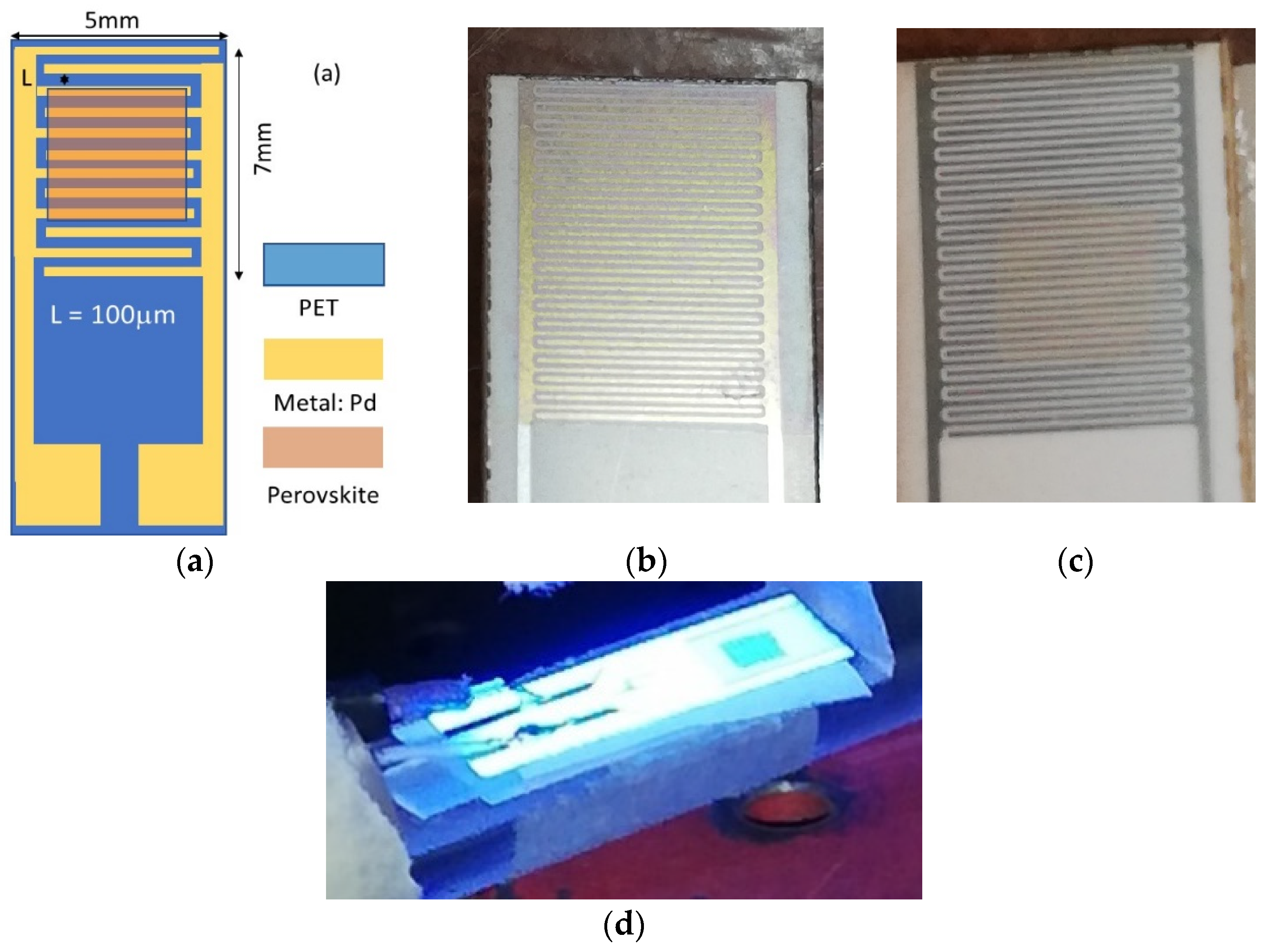
Figure 2.
500 nm-thick CsPbCl3 film grown on a soda–lime glass substrate using RF magnetron sputtering. (a) SEM micrograph. (b) XPS analysis as a function of the exposure time. (c) XRD spectra: blue line corresponds to θ–2θ configuration, red line corresponds to grazing incidence, black bars correspond to identified lines of the tetragonal phase according to ICDD PDF-47 18-0366.

Figure 3.
Optical characterization of a 500 nm-thick CsPbCl3 film on a soda-lime glass substrate. (a) Plot of the function (αhν)2 vs. energy and linear fit used to evaluate the bandgap. (b) Low and high-temperature PL. (c) PL quenching fitted to an Arrhenius law obtained considering two activation energies, E1 and E2, with probability amplitudes A1 and A2, respectively.

Figure 4.
(a) Current density vs. voltage measured in the dark at room temperature with three photodetectors characterized by the presence of CsPbCl3 films on the interdigitated electrodes with different thicknesses and areas: t1 = 1000 nm, t2 = 500 nm, A1 = 5 × 7 mm2, A2 = 3 × 3 mm2. (b) Current–voltage characteristics of a film with thickness t2 and area A2 within the 0–20 V range, fitted with a parabolic curve.

Figure 5.
Room temperature I-V characteristics of a photodetector with a CsPbCl3 film of thickness t1 and area A1 under stationary illumination from a 365 nm LED with varying intensities and in the dark.
Figure 5.
Room temperature I-V characteristics of a photodetector with a CsPbCl3 film of thickness t1 and area A1 under stationary illumination from a 365 nm LED with varying intensities and in the dark.

Figure 6.
Room-temperature I–V characteristics of a photodetector carrying a CsPbCl3 film of thickness t1 and area A1 under illumination with LEDs of different wavelengths at the same intensity, 25 W/m2, and in the dark.
Figure 6.
Room-temperature I–V characteristics of a photodetector carrying a CsPbCl3 film of thickness t1 and area A1 under illumination with LEDs of different wavelengths at the same intensity, 25 W/m2, and in the dark.

Figure 7.
I–t characteristics of a photodetector carrying a CsPbCl3 film with thickness t2 and area A1 under 250 W/m2 illumination using a 365 nm LED at a pulse rate of 10 Hz. Supply voltage was 10 V.
Figure 7.
I–t characteristics of a photodetector carrying a CsPbCl3 film with thickness t2 and area A1 under 250 W/m2 illumination using a 365 nm LED at a pulse rate of 10 Hz. Supply voltage was 10 V.

Figure 8.
I–t characteristics of a photodetector carrying a CsPbCl3 film of thickness t2 and area A2 under 500 W/m2 illumination using a 365 nm LED at pulse rate of 90 Hz. Supply voltage was 30 V.
Figure 8.
I–t characteristics of a photodetector carrying a CsPbCl3 film of thickness t2 and area A2 under 500 W/m2 illumination using a 365 nm LED at pulse rate of 90 Hz. Supply voltage was 30 V.

Figure 9.
I-t characteristics of a photodetector with a CsPbCl3 film of thickness t2 and area A1 under 500 W/m2 illumination using a 365 nm LED at pulse rate of 0.1 Hz. Supply voltage was 15 V.
Figure 9.
I-t characteristics of a photodetector with a CsPbCl3 film of thickness t2 and area A1 under 500 W/m2 illumination using a 365 nm LED at pulse rate of 0.1 Hz. Supply voltage was 15 V.

Figure 10.
Photoconductivity signal ΔI = I − Idark plotted as a function of the incident power P on a photodetector with a CsPbCl3 film with an area of A1 and a thickness of t1. Linear best-fit added to obtain the responsivity R.
Figure 10.
Photoconductivity signal ΔI = I − Idark plotted as a function of the incident power P on a photodetector with a CsPbCl3 film with an area of A1 and a thickness of t1. Linear best-fit added to obtain the responsivity R.

Figure 11.
Amplitude of the Fourier Transform function obtained from the analysis of the photocurrent responses shown in Figure 7 and Figure 8, plotted as a function of the frequency for 10 Hz and 90 Hz squared pulses with a 50% duty cycle.

Figure 12.
Current response of the CsPbCl3 photodetector to a 50 ms pulse illumination at 250 W/m2 using a 365 nm LED. Supply voltage was 10 V.
Figure 12.
Current response of the CsPbCl3 photodetector to a 50 ms pulse illumination at 250 W/m2 using a 365 nm LED. Supply voltage was 10 V.

Disclaimer/Publisher’s Note: The statements, opinions and data contained in all publications are solely those of the individual author(s) and contributor(s) and not of MDPI and/or the editor(s). MDPI and/or the editor(s) disclaim responsibility for any injury to people or property resulting from any ideas, methods, instructions or products referred to in the content. |
© 2023 by the authors. Licensee MDPI, Basel, Switzerland. This article is an open access article distributed under the terms and conditions of the Creative Commons Attribution (CC BY) license (https://creativecommons.org/licenses/by/4.0/).
Share and Cite
MDPI and ACS Style
Bruzzi, M.; Falsini, N.; Calisi, N.; Scardi, P.; Vinattieri, A. Photoconductive Response to Pulsed UV Light of CsPbCl3 Flexible Thin Films Grown by Magnetron Sputtering. Coatings 2023, 13, 1128. https://doi.org/10.3390/coatings13061128
AMA Style
Bruzzi M, Falsini N, Calisi N, Scardi P, Vinattieri A. Photoconductive Response to Pulsed UV Light of CsPbCl3 Flexible Thin Films Grown by Magnetron Sputtering. Coatings. 2023; 13(6):1128. https://doi.org/10.3390/coatings13061128
Chicago/Turabian StyleBruzzi, Mara, Naomi Falsini, Nicola Calisi, Paolo Scardi, and Anna Vinattieri. 2023. "Photoconductive Response to Pulsed UV Light of CsPbCl3 Flexible Thin Films Grown by Magnetron Sputtering" Coatings 13, no. 6: 1128. https://doi.org/10.3390/coatings13061128
Note that from the first issue of 2016, this journal uses article numbers instead of page numbers. See further details here.