Review

Recent Progress in Electrohydrodynamic Jet Printing for Printed Electronics: From 0D to 3D Materials

1
State Key Laboratory of High-Performance Precision Manufacturing, School of Mechanical Engineering, Dalian University of Technology, Dalian 116024, China
2
Department of Electrical and Computer Engineering, The University of Alabama, Tuscaloosa, AL 35487, USA
3
Department of Electrical and Computer Engineering, Penn State Behrend, Erie, PA 16563, USA
*
Authors to whom correspondence should be addressed.
Coatings 2023, 13(7), 1150; https://doi.org/10.3390/coatings13071150
Submission received: 28 April 2023 / Revised: 7 June 2023 / Accepted: 17 June 2023 / Published: 25 June 2023

Abstract

:
Advanced micro/nano-flexible sensors, displays, electronic skins, and other related devices provide considerable benefits compared to traditional technologies, aiding in the compactness of devices, enhancing energy efficiency, and improving system reliability. The creation of cost-effective, scalable, and high-resolution fabrication techniques for micro/nanostructures built from optoelectronic materials is crucial for downsizing to enhance overall efficiency and boost integration density. The electrohydrodynamic jet (EHD) printing technology is a novel additive manufacturing process that harnesses the power of electricity to create fluid motion, offering unparalleled benefits and a diverse spectrum of potential uses for microelectronic printing in terms of materials, precision, accuracy, and cost-effectiveness. This article summarizes various applications of EHD printing by categorizing them as zero-dimensional (0D), one-dimensional (1D), two-dimensional (2D), and three-dimensional (3D) printing materials. Zero-dimensional (quantum dot) materials are predominantly utilized in LED applications owing to their superb optoelectronic properties, high color fidelity, adjustable color output, and impressive fluorescence quantum yield. One- and two-dimensional materials are primarily employed in FET and sensor technologies due to their distinctive physical structure and exceptional optoelectronic properties. Three-dimensional materials encompass nanometals, nanopolymers, nanoglass, and nanoporous materials, with nanometals and nanopolymers finding widespread application in EHD printing technology. We hope our work will facilitate the development of small-feature-size, large-scale flexible electronic devices via EHD printing.

1. Introduction

High-resolution micro/nano-flexible sensors, displays, electronic skin, and related devices possess significant advantages over traditional technologies which help to promote the miniaturization of devices [1,2,3], improve their energy efficiency, and increase system stability [4,5,6]. Developments in high-resolution, scalable, and inexpensive micro/nano-structure fabrication technologies for optoelectronic materials are essential for the size reduction necessary to improve performance and increase integration density. Additive micro/nano-manufacturing shows significant advantages over traditional subtractive manufacturing techniques, such as photolithography, particularly in its ability to manufacture microstructures, substrates, and fabricate devices at greater rates [7,8,9,10,11,12,13,14,15]. Additive manufacturing techniques for micro/nano technologies mainly include inkjet printing, photocuring molding, micro-stereolithography, two-photon polymerization, micro-laser sintering, selective laser melting, and electrohydrodynamic (EHD) printing [16,17,18,19,20].
Inkjet printing is advantageous for printing flat patterns due to its additive nature, wide coverage, low temperature requirements, and cost-effectiveness [21,22]. These advantages have thus been applied to the fabrication of microelectronic components, proving inkjet printing as an effective electronic fabrication technology for the manufacture of electronic devices such as transistors, light-emitting diodes, and sensors [23,24,25]. This manufacturing technique also has a wide range of applications in optical, electrical, and biological devices [26]. The use cases of inkjet printing in the production of advanced devices are therefore diverse; however, the more complex nozzle structure required for these applications imposes strict requirements for physical parameters such as ink viscosity, solute particle size, and nozzle size [27,28,29]. Poor ink quality can be a significant contributing factor to the clogging or breaking of a printer head. Additionally, current nozzles are limited to a minimum inner diameter of approximately 10 μm, constraining the resolution of printed 3D structures to physical dimensions which are also on the order of ten microns and therefore presenting an obstacle to the manufacturing of finer structures [30,31,32,33]. Although photocuring molding technology and micro-stereolithography can print complex structures with high molding accuracy, they are only applicable to photosensitive materials or photosensitive resin materials [34]. These technologies also demand the implementation of expensive equipment which limits their further development [30,35,36,37,38,39,40,41,42,43,44]. Two-photon polymerization and micro-laser sintering technologies possess the same disadvantages of high cost, low efficiency, and a limited pool of applicable materials with which to develop devices. By contrast, inkjet printing of electronic devices presents advantages such as a simple manufacturing process, suitability for bendable surfaces, compatibility with wide-area substrates, and low production costs [22,45,46,47,48,49,50,51].
Instead of pushing the printing material out of the nozzle like traditional printing methods, EHD jet printing uses high electrical fields to pull the material out. EHD printing can create precise micro- and nano-manufactured products [52,53,54,55]. By applying an electric potential between the nozzle and substrate, charged particles gather at the liquid–air interface, causing the meniscus to transform into a conical shape known as the Taylor cone. Once the electrostatic forces exceed the surface tension, extremely thin droplets are released from the Taylor cone with accuracy better than one-thousandth of the nozzle’s orifice, resulting in superior printing resolution (<1 μm) [56,57,58,59,60,61,62,63,64,65,66,67]. Thin film layers can also be created via EHD printing by adjusting the ink characteristics and process conditions. The level of precision and control EHD printing offers makes it an attractive option for micro- and nano-manufacturing, especially for intricate patterning achieved by moving the receiving substrate in both the x- and y-axis directions under the jet head [68,69,70,71,72]. EHD jet printing now has a rich system of applicable manufacturing materials [17,73], and although researchers have summarized the manufacturing process and industry applications of EHD jet printing, analyses of this technology’s associated printing materials are still scarce [74,75,76,77,78,79]. Therefore, a comprehensive and systematic review of this technology’s implementable printing materials is urgently needed [80,81,82,83,84].
In this review paper, we have summarized the most recent work on EHD jet printing, highlighting the roles that different dimensional functional ink (0-, 1-, 2-, and 3-D materials) play in EHD jet printing, and summarizing the advantages and disadvantages of each material. Finally, we also demonstrated the foreseeable difficulties and possibilities of advanced E-jet printing technology in the context of creating malleable electronic devices [85,86,87].

2. Advanced EHD Printing Technology

Zero-dimensional materials, also referred to as quantum dot (0D) materials, have the capacity to modify their optical properties depending on the size of the material, allowing for large-scale production while maintaining low cost [52]. The result is a steady and efficient emitter of almost any wavelength after decades of research and development. One-dimensional nanomaterials are ideal for the study of electron transport behavior, optical properties, and mechanical properties due to their high aspect ratio. Moreover, in the preparation of nanoscale devices, such materials can take on a significant role in the implementation of interconnects between disparate devices, such as field-effect tubes. Two-dimensional materials distinguish themselves from other bulk materials because of their unique planar structure and large specific surface area. These materials are projected to become revolutionary materials of the future due to their outstanding characteristics, including their single atomic layer construction and high carrier mobility. Common 3D nanomaterials include nanometal particles and nanopolymers. Nanocrystalline metal materials have received special attention due to their excellent properties, in particular their high strength, high resistivity, and good plastic deformation [88,89,90,91,92,93,94,95]. Each set of varying dimensional materials exhibits its own excellent characteristics, but at their present state of research and development, each exhibits its own problems as well. One of the common difficulties associated with these materials is the ability to place small functional materials at a desired location [73,87,96,97,98]. The storage conditions for different printing materials will vary, but they all have a common storage feature that requires centrifugal agitation ranging from 1 to 24 h, and the solution needs to be placed in a stable environment to ensure stable solution performance, to make sure that surface tension, homogeneity, and functionality do not change in any way. Insulating materials are materials that do not conduct electricity under the allowed voltage, but are not absolutely non-conductive materials; under the action of a certain applied electric field strength, conductive, polarization, loss, breakdown, and other processes will occur. The EHD printing technology also involves the printing of insulating materials, such as PVA, PDMS, MOS2, etc.; when a relatively high voltage is applied to these materials, an electric charge will be generated, the formation of a Taylor cone will occur, and then a jet to achieve the EHD printing process.
The EHD printing technology is employed in the fabrication of high-resolution flexible electronics composed of materials of various dimensions as a result of its diverse material compatibility [99]. This paper summarizes EHD printing technology in terms of 0D, 1D, 2D, and 3D materials [88]. A range of functional materials have been utilized recently in E-jet printing to produce diverse flexible electronic devices (Figure 1a). Figure 1b summarizes the four-dimensional functional inks discussed in this paper. Additionally, a summary of common printing materials and their associated properties (applications, printing substrates, and material advantages) is provided in Table 1. The work on EHD printing is presented in terms of the preparation of patterned electrodes, sensors, field-effect transistors (FETs), and light-emitting diodes (LEDs) [34]. The storage conditions for different printing materials will vary, but they all have a common storage feature that requires centrifugal agitation ranging from 1 to 24 h, and the solution needs to be placed in a stable environment to ensure stable solution performance, and to make sure that surface tension, homogeneity, and functionality do not change in any way.
The process of EHD printing uses a high-strength electric field force to pull the printing material out of the nozzle, as opposed to traditional printing processes which push the material out of the nozzle to form small droplets [89,90]. The process of EHD printing involves using an electric field to create a Taylor cone, which is achieved by applying a potent electric force between the substrate and the nozzle tip. This results in the liquid being expelled from the nozzle in the form of a Taylor cone. As the charge force surpasses the liquid’s surface tension, it forms seamless jet lines that are deposited onto the substrate. Moreover, intricate three-dimensional (3D) micro/nano designs are produced by synchronizing the movements of the plate bearing table (X–Y direction) and the nozzle table (Z direction) (Figure 1c) [100]. EHD printing offers advantages for micro- and nano-manufacturing due to its precision printing capabilities. The possibility of applying an electric potential between the nozzle and the substrate leads to a gathering of movable charged particles near the interface between the liquid and the air surface, causing the meniscus to be altered into a conical shape known as a Taylor cone [91,92,121]. When the electrostatic stresses surpass the surface tension of the meniscus, an extremely narrow stream of droplets is ejected from the Taylor cone with an accuracy better than one-thousandth of the nozzle’s orifice, resulting in superior printing resolution (<1 μm). Furthermore, the ink characteristics and process conditions can be tuned in order to create thin film layers via electrospraying [122,123,124]. This level of precision and control makes EHD printing an attractive option for all types of micro- and nano-manufacturing. EHD jetting lends itself to the implementation of intricate patterning, which can be obtained by moving the receiving substrate under the jet head in both x- and y-axis directions as shown in Figure 1d–f. Comparisons of EHD printing with other printing technologies are shown in Table 2.

3. Zero-Dimensional Materials for EHD

Due to their unique physical and chemical properties, 0D materials have a wide range of promising applications in various fields. Since the size of quantum dots is very close to their corresponding energy wavelengths, they can be used as light-emitting materials and thus have a wide range of applications, such as display technology, LEDs, bio-imaging, etc.

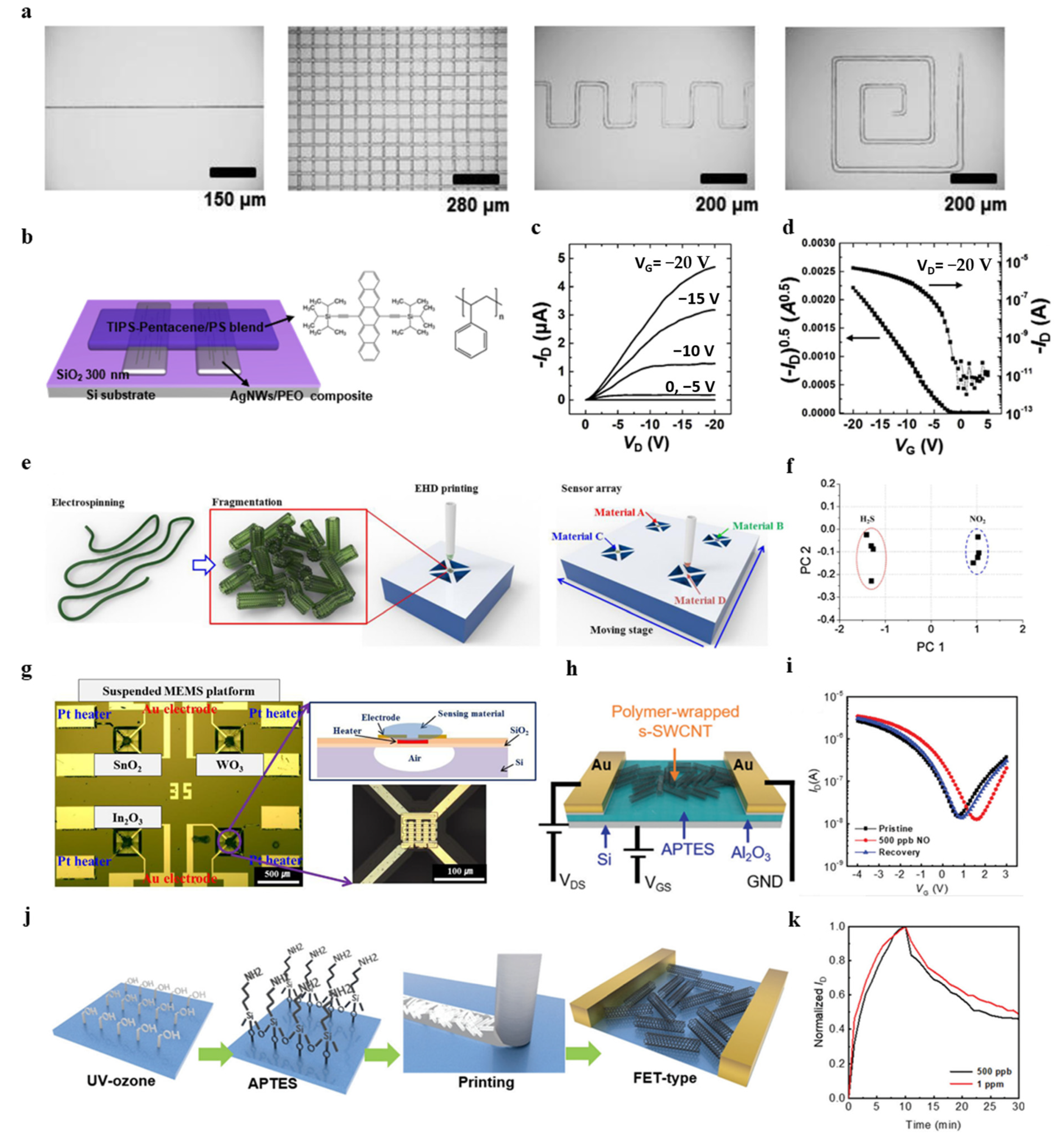
3.1. Luminous Device Printing by EHD

Quantum dot technology presents excellent photoelectric properties, including superior color accuracy, adjustable wavelengths of luminescence, and a high fluorescence quantum yield. As a result, quantum dot devices have become a very important class of luminescent materials and have experienced widespread application in EHD printing. Kress et al. [103] synthesized two types of quantum dots, namely CdSe/ZnS and CdSe/CdS core/shell nanocrystals. Utilizing EHD printing, they were able to produce highly fluorescent QD patterns on both planar and structured substrates with nanoscale accuracy, sub-diffraction resolution, and customizable colors, shapes, and intensity levels. Furthermore, Kim et al. [102] used EHD jet printing in the implementation of active layers of quantum-dot (QD) LEDs. The inks were composed of dilute solutions of 0.25% of various types of QDs, such as cadmium selenium/cadmium zinc selenide sulfide (green) and cadmium selenium/cadmium sulfide/zinc sulfide (red) core/shell quantum dots, in dichlorobenzene. Figure 2a displays QD-LEDs created using EHD-printed patterns of QDs. These devices consist of (i) an anode layer of ITO on a glass substrate, (ii) a hole injection layer of poly(3,4-ethylenedioxythiophene) polystyrene sulfonate (PEDOT/PSS), (iii) a hole transport layer of thin film battery (TFB), (iv) emission of green or red QDs, (v) an electron transport layer of ZnO, and (vi) a cathode layer of Al that is evaporated using an electron beam. Figure 2b,c depict an optical microscope image and a schematic of a metal-plated glass nozzle (inner diameter of 5 μm at the tip) and a printing medium on which the ink is applied, respectively. Figure 2d shows an array of green QDs lines on (Type I device) and a pattern of green and red quantum dots arranged in an alternating array (Type II device). Figure 2e,f exhibit fluorescent and photographic representations, correspondingly, of Type I and Type II apparatuses operating at a voltage of 4 V. In both devices, the separate EL emission from every layer of the quantum dots is visibly present. However, in Type I, the green emission is observed to be weaker than the red emission, as illustrated in Figure 2g. This is further confirmed with voltage readings, as seen in Figure 2h, where the peak of the normalized green and red EL intensity can be found. As Figure 2i illustrates, the EL spectra of Type II devices have been normalized. Moreover, from Figure 2j, one can observe that the intensities of green and red light emitted by Type II devices are comparable. Altintas et al. [129] described the formation of nanocrystals of CsPbBr3 and CsPbBrxI3−x through synthesis, as shown in Figure 2k. These nanocrystals have photoluminescence yields as high as 91% with emission linewidths of 15 nm, making them appropriate for creating high-quality white light, as shown in Figure 2l. The researchers printed linear and dot patterns of synthesized and anion-exchanged PNCs, which exhibited strong and localized photoluminescence (shown in Figure 2m,n). Moreover, they utilized EHD jet printing to generate narrowly positioned lines of variously shaded PNCs, which they then integrated with a blue LED, resulting in the production of a white LED. The process is illustrated in Figure 2o–q. The LED displayed outstanding photometric qualities, demonstrating a color rendering index of 91.3, optical radiation luminous efficacy surpassing 300 lm/Wopt, and a correlated color temperature of approximately 7000 K (as depicted in Figure 2r). Besides printing single-dot quantum dot materials, EHD printing technology can also be used to prepare thin films of quantum dots. Tuan et al. [130] proposed a novel EHD spraying mechanism that utilizes CdSe/CdS/ZnS colloidal QD thin films for the development of high-performance LED lighting. The dimensions of the quantum dot droplets were regulated systematically through the stable electrospray mode generated by EHD from a solvent mixture, which is essential for the creation of extensive and seamless layers of quantum dot materials. The team successfully reduced material usage through the innovative use of a coating system. Their electrodeposited QD-based QD-LED device achieved impressive results, including a maximum luminance of 12,082 cd m−2, a maximum current efficiency of almost 4.0 cd A−1, and a maximum external quantum efficiency (EQE) of 1.86%.

3.2. FETs and Sensors

In addition to applications in LED production, quantum dot materials can also be used in the manufacture of sensors and FETs via EHD printing. Matthias et al. [106] utilized EHD jetting as a printing method to deposit colloidal PbS quantum dots onto six GFETs, with different thicknesses of QD layers on a single substrate. The resulting QD films exhibited uniformity, thanks to a spatial resolution of nanoprinting that was less than 1 µm. Additionally, the PbS/graphene phototransistors displayed exceptional responsivities exceeding 104 AW−1. Figure 2u displays an AFM image of quantum dots (QDs) exhibiting pillar features sized at 700 nm, with a mean height of 107 nm, and a typical deviation of 10 nm. The device structure (Figure 2t) showcases the mechanism of generating electron and hole pairs generated in the PbS quantum dot thin film upon exposure to light, followed by the separation and transfer of charge carriers. In this process, one carrier type tends to migrate more rapidly toward the biased graphene field-effect transistor (GFET), causing a modification in the electric field existing between the layers of graphene and QDs. The conductance of the GFET is used to measure the modification resulting from the QD layer thickness, which is reflected in a change in conductance. However, as shown in Figure 2v, the normalized noise current is not impacted by the thickness of the QD layer. This indicates that the noise is primarily associated with the interface between graphene and SiO2. Therefore, using different substrate materials could significantly reduce the noise. The trend of responsiveness shows an ideal thickness for the QD layer of 130 nm, which can achieve a specific detectivity of at least 109 Jones.

4. One-Dimensional Materials for EHD

One-dimensional materials have excellent electron transport properties and can have a wide range of applications in electrical conductivity and sensors due to their local seriality and high surface-area-to-volume ratio. In addition, 1D materials also exhibit excellent optical properties, such as carbon nanotubes can be used as solar cell modules to improve the efficiency of solar cells, and can also be used in other related fields of development.

4.1. Electrodes

One-dimensional nanomaterials such as gold nanowires (AuNWs), silver nanowires (AgNWs), and copper nanowires (CuNWs), which can be made into conductive inks that possess high electrical conductivity, are employed in EHD jet printing technology. When it comes to EHD printing ink, AgNWs are the more suitable option due to their superior conductivity, lower price, and ability to withstand oxidation, in contrast to AuNWs and CuNWs. EHD printing has the capability to precisely print the conductive materials needed for the formation of electrodes, which enables the production of patterns of electrodes with high resolution. This is highly beneficial in terms of creating high-performance circuits and achieving a high integration of electronic devices. In order to fabricate silver electrical traces on a flexible Kapton substrate by inkjet printing, Wu et al. [131] produced a binary hybrid ink by adding silver nanowires to silver nitrate. When 20% of the mixed ink was utilized, the silver conductive lines were subjected to ethylene glycol fumes at a temperature of 200 °C for an hour. The resulting resistivity of 7.31 × 10⁻⁵ Ω cm was similar to that of bulk silver. Jeong et al. [132] fabricated multi-walled carbon nanotube (MWCNT)/polystyrene sulfonate (PS) composites by printing them onto surfaces that were modified with PS brushes. They successfully printed this ink using EHD techniques and observed electrical conductivity in the printed lines with a maximum value of 39.3 S cm−1. Four distinct jetting modes were obtained based on the voltage level and distance of operation. Multi-walled carbon nanotubes (MWCNT) and poly(4-styrenesulfonic acid) (PSS) were employed as the source/drain (S/D) electrodes in organic field-effect transistors (OFETs), forming conductive lines. The OFETs produced reliable results and showed little hysteresis when utilized on PS-brush-modified surfaces treated with chlorosilane.
A transistor is a vital part of a flexible device such as a high-resolution display device. To ensure the smooth functioning of a device, it is crucial to have excellent electrical performance. The stability of electrical performance is ensured by the transistors produced through E-jet printing. Li et al. [106] examined the EHD printing process for silver nanowire (AgNW) ink. The printing of AgNW/polyethylene oxide (PEO) (90:10) composite resulted in clear and distinct designs with different forms and a printed line width of approximately 27 μm at the optimal printing conditions (Figure 3a). These EHD-printed AgNW/PEO composites were utilized as the source/draining (S/D) electrodes for bottom-contact TIPS–pentacene blend organic thin-film transistors (OTFTs) (Figure 3b). Figure 3c,d displays the output and transfer characteristics, respectively, in terms of the plots of ID-VD and ID-VG characteristics for bottom-contact organic thin-film transistors (OTFTs). The use of a TIPS–pentacene mixture results in OTFTs with an average μFET of approximately 0.51 cm2/Vs, Vth of −2.5 V, and an Ion/Ioff ratio of 106. Similarly, Ye et al. [109] created a homogeneous and highly soluble solution composed of zinc acrylate and tin-chloride precursors. This homogeneity was seen in the zinc–tin–oxide (ZTO) precursor ink, which was ideal for EHD printing to make thin-film transistors (TFTs) using pre-patterned ZTO samples on which multi-walled carbon nanotubes (MWCNTs) were printed as source/drain electrodes. This EHD-printed TFT had a field-effect mobility of 0.52 ± 0.08 cm2/Vs.

4.2. Sensors

The E-jet printing method is an affordable, mask-free manufacturing technique that allows for the direct printing of pliable and elastic conductor materials, facilitating the creation of precise and versatile flexible devices. Utilizing this method, various kinds of sensors, including temperature sensors, touch sensors based on capacitive technology, and gas sensors, can be fabricated. A technique for creating micro-patterns of metal oxide nanofibers was devised by Kang et al. [105] utilizing the EHD printing process for electrospun fibers. The electrospinning process was used to create nanofibers composed of SnO2, In2O3, WO3, and NiO. Subsequently, ultrasonication was utilized to break down these nanofibers into smaller pieces, which were then dissolved in organic solvents. Through the optimization of printing parameters, they succeeded in producing microscale designs of electrospun nanofibers that measured less than 50 μm in diameter. These designs were subsequently utilized in the manufacturing of gas sensors. EHD printing was employed to produce microelectrode-based gas sensors that can sense harmful gases, including NO2, CO, and H2S, even when present at extremely low levels (as shown in Figure 3e). Four different metal oxides were tested and shown to detect NO2, H2S, and CO gases at levels as low as 0.1, 1, and 20 ppm, respectively. Furthermore, Figure 3g illustrates an array of low-power SnO2, WO3, and In2O3 nanofiber gas sensors deposited on a suspended MEMS microheater platform. These three materials were arranged in microscale patterns to form a sensor array without causing any harm to the MEMS bridge-plate framework. Tang and colleagues [107] explored an easy-to-use pulling method for EHD printing of an ink containing semiconducting single-walled carbon nanotubes (s-SWCNTs) coated with polymer onto Si substrates with Al2O3 (50 nm) as a layer. The initial step involved cleaning the substrates to eliminate hydroxyl groups that serve as sites for charge trapping. Afterward, the substrates were subjected to APTES treatment as a means of passivating the hydroxyl groups. Figure 3f depicts the reactions of NO2 (0.1 ppm) and H2S (10 ppm) with SnO2, WO3, and In2O3 nanofibers, displayed with two primary components. The EHD printing process was used on APTES-treated surfaces to form PFDD-wrapped s-SWCNTs (The objective was to optimize the alignment and dispersion of PFDD-s-SWCNT lines, with the aim of achieving optimal printing conditions and ensuring strong interconnectivity. This method was also used for fabricating NO-gas-sensing FETs (Figure 3h). The FETs that employed polymer-coated s-SWCNTs showed an average mobility of 2.939 cm2 (V−1 s−1), a threshold voltage of 2.21 V, an on/off ratio of around 103, and a subthreshold swing of 0.968 Vdec−1. Figure 3h–k depict alterations in the transfer characteristics of the FETs when exposed to NO gas levels of 500 ppb, and changes in the normalized response at NO levels of 500 parts per billion and 1 part per million.

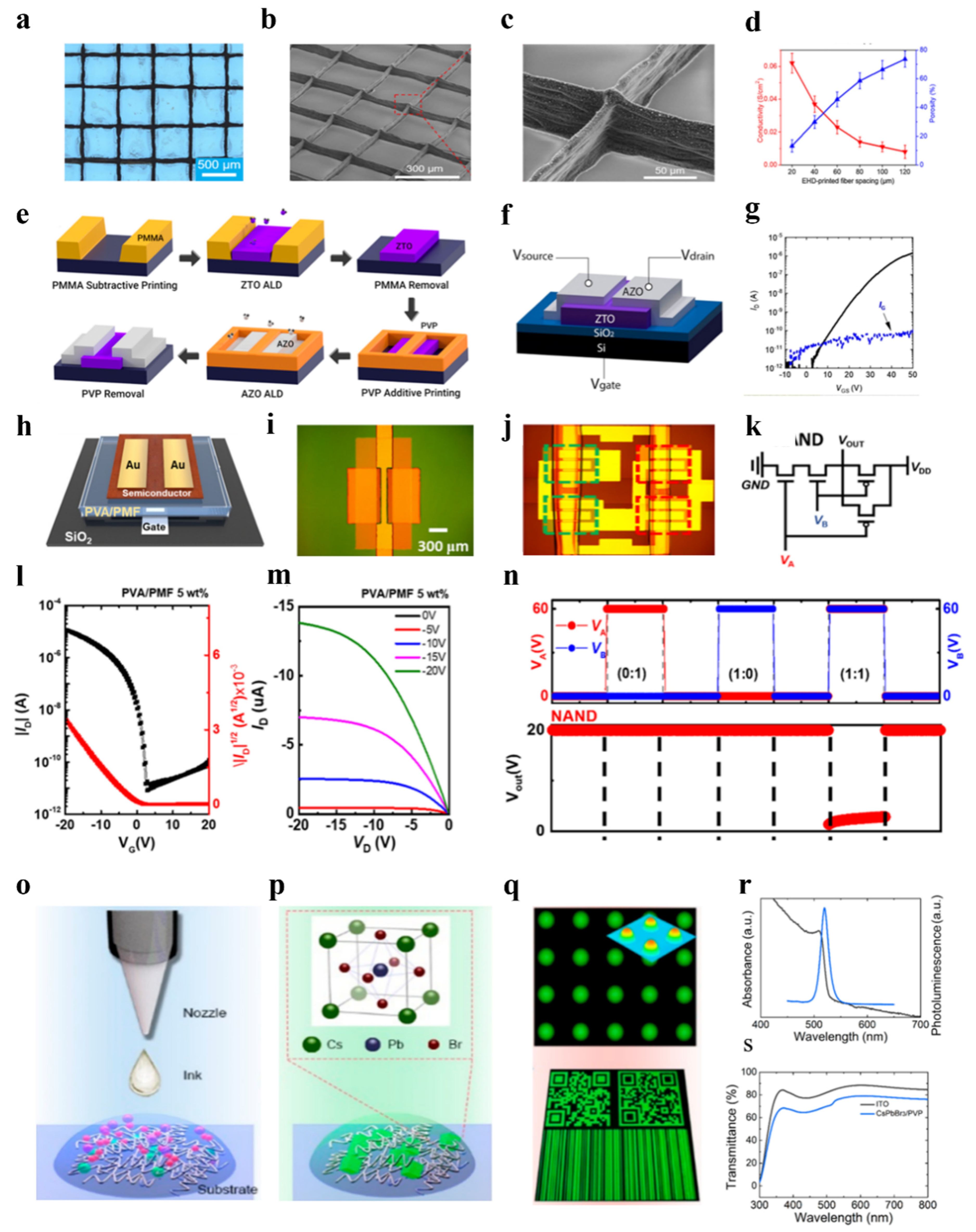
5. Two-Dimensional Materials for EHD

Two-dimensional materials are two-dimensional crystals that are only a few atomic layers thick, such as graphene and molybdenum disulfide. Due to their extreme thinness, they exhibit a strong thickness effect, which imparts unique electrical, optical, mechanical, and physical properties to the materials. Two-dimensional materials possess high carrier mobility and large carrier concentrations, and thus hold promise for a wide range of applications in electrical conductivity, memory, and sensors.

5.1. Patterns and Electrodes

Since graphene, a 2D material, was discovered, there has been a great deal of scientific interest in 2D layered materials due to their numerous interesting physical properties, not present in their 3D counterparts. Graphene provides many benefits, such as a large surface area, high chemical resistance, and outstanding electrical conductivity, making it particularly suitable for flexible microelectronic applications such as electrochemical sensors and energy storage. In order to take advantage of its unique benefits, Li et al. [109] developed and implemented an instrument to precisely manipulate EHD printing with current measurement. Utilizing this procedure, uniform nanoscale graphene patterns were produced under the observation of a real-time monitoring and control process. Likewise, Zhao et al. [133] developed a microscale graphene patterning method via EHD printing employing micro-dripping through the application of pulsed voltage. These complex graphene microscale structures were printed in a single step. By adjusting the pulsed voltage parameters, the width and depth of the graphene patterns were regulated. After 20 printings, the resistivity of the graphene lines was found to be low, with an approximate value of 1.1 mΩ·cm. The EHD technique was employed to fabricate microelectrodes made of graphene/Pt (G/Pt), by depositing a precisely printed layer of graphene onto pre-existing Pt microelectrodes. The resulting G/Pt microelectrodes demonstrated exceptional sensitivity. Wan et al. [110] employed the EHD technique to directly print reduced graphene oxide (RGO) suspensions and thereby achieved the generation of complex, electrically conductive geometries with high resolution (line width of ~5 μm). Such high-precision printing of RGO was accomplished not only on planar surfaces but also on curved surfaces with a small curvature radius (50–65 μm).

5.2. Thin-Film Transistor (TFT)

There are many materials that are used in TFTs through EHD printing technology. Can et al. [111] proposed a novel EHD jet printing approach for synthesizing MoS2 from a precursor solution of (NH4)2MoS4, which was demonstrated for the first time. This method resulted in patterns that exhibited a uniform and seamless surface (with an Rq value of 0.2 nm) and possessed a small pattern size (with a width of 150 μm). Printed multilayer MoS2 was used as the active layer and Al was utilized as inexpensive source/drain electrode material in constructing transistor field-effect devices (TFTs). These devices showed n-type behavior and had a high on-to-off current ratio of 5.0 × 10⁶, a low subthreshold voltage of 1.9 V/dec, and field-effect mobility of 19.4 cm2/Vs. Additionally, using a sol–gel precursor solution with an EHD jet printing process and one-step thermolysis process, Can et al. [134] successfully created smooth and uniform MoS2 line patterns measuring only 60 μm in width, with a surface roughness value (Rq) of approximately 0.19 nm. Furthermore, economical Al was utilized as the source/drain electrode material, while utilizing a high-dielectric constant gate insulator of Al2O3 to successfully produce high-performance TFTs that lack any wrinkles in the printed multilayer MoS2 active layer. The TFTs exhibited exceptional electrical characteristics, such as a rapid switching rate and first-class field-effect mobility (47.64 ± 2.99 cm2/Vs). The average trap density state demonstrated a strong correspondence with the interface of MoS2/Al2O3. This fact permits the implementation of high-current devices. Similarly, Tang et al. [113] successfully accomplished the patterning of large-area MXene electrodes by employing a programmed electrohydrodynamic (EHD) printing procedure. In order to determine the precision of MXene nanosheets, they were used as the gate and S/D electrodes for their printed thin-film transistor (TFT) and inverter devices. Achieving stable operation and acceptable performance, these TFTs consisted of single-walled carbon nanotubes (SCNTs) and fluoropolymer/vinylidene fluoride-hexafluoropropylene (FPVDF-HFP). With optimized conditions, a 5 mg mL−1 TFA-MX solution was injected into the EHD printing machine, as demonstrated in Figure 4a,b, enabling the direct printing of electrodes. Figure 4c,d demonstrate the transfer characteristics observed for p- and n-type organic thin-film transistors (TFTs), fabricated using the printed TFA-MX gate and S/D electrodes, respectively. In addition, An et al. [135] were able to fabricate complementary inverter, NAND, and NOR logic gates employing the patterned MXene electrodes produced using a straightforward printing technique.

5.3. Gas Sensors

The use of EHD printing technology to prepare components for gas sensors is now well established. Zhang and colleagues [136] showed that the EHD jet printing method can be utilized to self-assemble layer-by-layer graphene oxide (GO). It was observed that GO flake alignment was mainly driven by flow- and electric-field-induced orientations that occurred along the jet’s path. Furthermore, evaporation-driven assembly at the water/air interface enabled the fabrication of highly homogenous laminar structures on the substrate (Figure 4e). Figure 4f displays a reduced graphene oxide (r-GO)-based supercapacitor and a 3D metal grid amalgamated ammonia sensor created using this method. Figure 4g,h demonstrates the top and cross-sectional view of the sensor structure with the metal grid fully covered by a stand-alone LBL r-GO film. Figure 4i illustrates the sensor’s response when exposed to varying concentrations of ammonia from 10 ppm to 50 ppm. The detection capabilities during two sequential periods of 2 min ammonia exposure and 3 min airflow are illustrated in Figure 4j.

5.4. Photoelectric Sensors

The use of EHD technology for the preparation of photoelectric sensors has been demonstrated in a much more instructive case. Alzakia and colleagues [112] employed an EHD printing method combined with ultrafast liquid exfoliation to create high-concentration inks (>2 mg/mL). These inks were used to fabricate photodetectors composed of MoS2 and WS2, and the graphene was utilized as the electrode material, all in one step. These sensors displayed light sensitivity down to 0.05 sun (Figure 4k). The current–voltage (IV) characteristics of the device with and without illumination are depicted in Figure 4l,m, respectively, from which it can be concluded that the low-resistance junction formed between MoS2/WS2 and graphene electrodes has been established. This printing technology can be used to prepare photoelectric sensors in a similar manner. Ali et al. [137] proposed a photodetector composed of a 120 nm thick graphene–perylene composite on a flexible substrate, which was fabricated utilizing EHD deposition. This sensor was equipped with comb-type silver electrodes spaced 50 μm apart, each with a width of 50 μm. The light sensor was capable of detecting a maximum brightness level of 400 lux and had sensitivity to wavelengths between 465 nm and 535 nm within the visible range. The active layer of the photodetector was transparent, and the sensor maintained its bendability capabilities up to a radius of 5 mm over a period of 1000 cycles, which makes it suitable for various transparent electronic applications with ITO electrodes. Ali et al. [138] introduced an extremely responsive sensor for measuring humidity, utilizing interlocking silver electrodes and a composite layer comprising graphene and methyl red (MR). This layered thin film was formed by electrophoretic deposition (EHD) on top of the silver interdigital electrodes, with a thickness of around 300 nm. The silver interdigital electrodes, as suggested, had a height of 400 nm, a finger width gap of 400 nm, and a length of 200 mm. As the RH increased from 5% to 95%, the sensor’s electrical resistance decreased from 11 MΩ to 0.4 MΩ.

6. Three-Dimensional Materials for EHD

Three-dimensional materials have become an indispensable type of material in industry and technology due to their high load-bearing capacity, ease of processing, and wide range of uses. It has been widely used in EHD printing technology.

6.1. Patterns and Electrodes

Gold nanoparticles (AuNPs), silver nanoparticles (AgNPs), and copper nanoparticles (CuNPs) in 3D form have significantly aided in the creation of flexible high-resolution electronic devices using EHD printing technology. These metal nanomaterials can be easily transformed into electrically conductive inks, which allows them to be readily used with EHD printing technology. Additionally, nanopolymers can also be utilized in this process. Yang and colleagues [114] utilized the EHD printing technique to fabricate a polyethylene-terephthalate-based flexible and transparent electrode composed of a silver grid (FTE). This led to the creation of an intricately precise design with a stroke width measuring 4.6 μm. Additionally, the FTE composed of a Ag grid boasted a resistance of approximately 4 Ω/sq, a transparency level of 80%, and a 150 μm pitch. Qin et al. [139] investigated the feasibility of utilizing EHD printing with silver nano ink to rapidly prototype capacitive touch sensors on flexible substrates. They tested a high-resolution humidity sensor from a 3D perspective and were able to demonstrate rapid prototyping of microelectrode arrays with a resolution of less than 20 μm on a polyethylene terephthalate (PET) film. By utilizing EHD jet printing with a drop-on-demand operation, Fariza et al. [140] accomplished uniform printing of silver dots (<10 μm) onto a silicon (Si) wafer with a minimal variation in diameter and thickness. Zhou and colleagues [141] investigated how the coffee ring effect operates on a nanoscale level, facilitating the production of a high-precision deposition pattern of Ag nanoparticles through EHD printing. Various shapes were produced with precise control, resulting in the creation of a ring featuring a line width in the sub-50 nm range. Similarly, Zhou et al. [141] successfully fabricated copper lines with a width of approximately 40 μm using a non-contact EHD printing process. After being sintered in a vacuum environment, the copper layer demonstrated a low resistivity of 8 × 10⁻⁴ Ωm, which differed from its resistivity after being annealed in air.

6.2. Conductive Patterns Prepared from Polymeric Materials

In addition to metal nanoparticles, polymer materials can also be used to print patterns and prepare electrodes. Li et al. [142] efficiently achieved detailed patterning and excellent crystalline forms of perovskite by mixing a thick perovskite precursor with polyvinylpyrrolidone (PVP) and utilizing EHD printing. Zhu et al. [143] achieved the fabrication of full-color perovskite patterns and a high-resolution dot matrix of 5 µm utilizing EHD printing, largely thanks to EHDs’ distinct benefits of intricate patterning at high resolution and extensive scalability, as well as the addition of PVP and the use of a postprocessing procedure with precisely tuned printing parameters. Duan et al. [144] achieved the effective fabrication of Cu lines with a width of approximately 40 μm using a noncontact EHD jet printing technique. The printed Cu layer showed reduced resistivity of 8 × 10⁻⁴ Ωm after sintering under vacuum instead of air annealing. Additionally, Jiang et al. [119] investigated the printing behavior of polydimethylsiloxane (PDMS)-based inks. To achieve optimal printing quality with well-defined network structures and parallel lines, various parameters, including pulse voltage, pulse frequency, droplet size, and printing frequency, were investigated to determine their impact on the printing process. Furthermore, Zhang and colleagues [145] utilized an EHD printing method to fabricate well-ordered C-Ni composite architectures for supercapacitor electrodes. The study aimed to examine the handling conditions through the use of polyacrylonitrile–Ni(NO3)2 fibers coated with a coating-by-coating deposition method to create 3D structures. Figure 5a shows an EHD-printed, 40-layer latticework with a 500 μm fiber gap. SEM images of the C-Ni 3D structures after carbonization are shown in Figure 5b,c. After going through the carbonization procedure, electrodes made of C-Ni with a minimum width of 9.2 ± 2.1 μm were produced. According to the electrochemical results, the C-Ni network electrode displayed a noticeably higher area-specific capacitance (2.3 times higher) and mass-specific capacitance (1.7 times higher) than the electrode fabricated through spin-coating. The higher specific capacitance per unit mass was explained by the combined effect of the structural porosity and electrical conductivity of the C-Ni electrodes, as presented in Figure 5d.

6.3. Transistors

Printing 3D materials to prepare transistors has also been shown to be feasible and very promising. Jung et al. [115] utilized EHD jet printing to produce a transistor utilizing an ion gel as a substrate. They employed both P3HT and PEDOT:PSS as the semiconductor and gate electrode, respectively. The printing process was successful and resulted in pattern widths of approximately 10 μm (for P3HT) and 200 μm (for PEDOT:PSS). The printed transistor displayed mean values of mobility (μ), threshold voltage (Vth), on/off current ratio (Ion/Ioff), and subthreshold swing (SS) that were 0.12 ± 0.05 cm2/Vs, −0.83 ± 0.1 V, around 105, and 73 ± 11 mV/decade, correspondingly. Additionally, Cho et al. [18] employed additive EHD printing to generate metal oxides that functioned as blockers for selective deposition of atomic layers in specific areas (AS-ALD), with an average width of 312 nm for the lines. Moreover, they exhibited the use of solvent inks in subtractive EHD printing, which dissolved polymer inhibitor layers in particular areas, enabling targeted AS-ALD within those areas. To demonstrate the production of 3D metal oxide formations through a combination of subtractive and additive printing techniques, they fabricated a ZTO TFT with a top contact and bottom gate, depicted in Figure 5e. The EHD and AS-ALD techniques were utilized to fabricate the device structure depicted in Figure 5f, and the process was completed successfully. The initial TFTs manufactured using these techniques exhibited exemplary performance, as illustrated in Figure 5g. The devices exhibited a turn-on voltage of 0 V, an on current above 1 μA, and an on/off current ratio greater than 105. Furthermore, the channel length of the devices was reduced to a minimum size of approximately 5 μm, which is ten times smaller than the previously achieved inkjet-printed inhibitors for AS-ALD. Min et al. [117] successfully produced highly aligned organic nanowires (ONWs) or nanofibers from polyvinyl-N-carbazole (PVK), semiconducting P3HT, and Polyera ActivInk N2200. They employed PVK as a shadow mask for organic nanowire lithography (ONWL) and used P3HT as the semiconductor layer in transistors. Through a combination of nanowire printing and ONWL, they achieved an impressive maximum μFET of 9.7 cm2/Vs (average μFE~3.8 cm2/Vs) in P3HT NW transistors, with a short channel length of approximately 300 nm and exceptionally low contact resistance (<5.53 Ω cm). Similarly, Jeong et al. [147] utilized EHD printing to directly create micropatterned lines of P3HT without the use of any polymer binder. These lines were used to form organic field-effect transistors, which exhibited high performance on substrates modified with octadecyl-trichlorosilane. The performance of these OFETs was comparable to that of other printed P3HT OFETs. Kim et al. [120] utilized poly[(1,2-bis-(2′-thienyl)vinyl-5′,5″-diyl)-alt-(9,9-dioctyldecylfluorene-2,7-diyl)] (PFTVT), an amorphous polymer, for the fabrication of an OFET array, employing EHD jet printing and spin-coating techniques. With meticulous adjustment of the printing conditions, the scientists could layer amorphous PFTVT chains in an orderly orientation as the operational layers for the OFET, leading to a μFET value that was five times greater than the most noteworthy μFET observed in spin-coated layers. Moreover, Jung et al. [118] included polyvinyl alcohol (PVA)-based components in an EHD printing approach to fabricate direct layouts of GI layers suitable for OFETs and complementary logic gates (Figure 5h–k). The EHD-printed PVA/poly(melamine-co-formaldehyde) (PMF) dielectric patterns were then deposited with p- and n-type organic semiconductors (OSCs). The fabricated OFETs performed reliably with decreased leakage currents (Figure 5i–m). The optimized PVA-based GIs with a PMF crosslinker enabled the preparation of complementary logic devices, such as inverters, and NAND and NOR gates, which all showcased reliable switching function and solid transmission operation without any hysteresis (as depicted in Figure 5m) and outstanding output characteristics in terms of saturation performance (as shown in Figure 5n).

6.4. Sensors

Sensors are important for many applications, including human life and industrial/medical/ecological monitoring, and printing 3D materials for preparing sensors has been widely used. Huang et al. [116] produced self-similar nano/microfibers of poly(vinylidene fluoride) (PVDF) using a combination of helix electrohydrodynamic printing (HE-printing) and surface self-organizing buckling. This method allows for the cost-effective, large-scale, and aligned regulation of the fibers. Furthermore, they suggested the use of self-replicating piezoelectric nano/microfibers to create a highly elastic, self-generating sensor (HSS) for practical applications, which showed superior mechanical stretchability of more than 300%, extremely low detection thresholds of less than 1 mg, and exceptional longevity of 1400+ cycles at 150% strain during stretching and releasing. Han et al. [148] utilized the EHD printing technique for producing touch sensor arrays with high density and resolution, utilizing molten metal inks, including Field’s metal (32.5% bismuth, 51% indium, and 16.5% tin), Wood’s metal (50% bismuth, 26.7% lead, 13.3% tin, and 10% cadmium), and solder (48% tin, 32% bismuth, and 20% lead). The sensor’s functioning is based on the alteration of the electric field by the presence of someone’s finger or by touching the tip. When a finger or another conductive object that is grounded touches the sensing tip, the fringing electric field of the sensor can be disturbed, resulting in a change in capacitance that can be measured as a touch signal.

6.5. Luminous Pattern

There are many other cases of luminescent patterns prepared from 3D materials. Liu et al. [146] successfully produced PVP nanocomposite microarrays with in situ crystallized perovskites with perfect morphologies. The ink was jetted onto substrates with a precision of 5 μm. When the perovskite precursor concentration reached its threshold for nucleation, CsPbBr3 nanocrystals were formed with a cube-shaped lattice structure after their ultimate crystallization at normal temperature through vacuum drying (Figure 5o,p). This strategy could easily be employed to produce different patterns, such as the ornate emblem of Fuzhou University, QR codes (Figure 5q), and a honeybee figure. The PL intensity of the microarrays composed of CsPbBr3 and PVP is enhanced as time elapses, as a result of the integration of CsPbBr3 nanocrystals into the PVP matrix, leading to the ultimate absorption and PL spectra illustrated in Figure 5r. The CsPbBr3/PVP microarrays appear to be nearly transparent when printed (as depicted in the inset of Figure 5s) and exhibit a 10% decrease in visible spectrum permeability (as shown in Figure 5s).
Similarly, to enhance the performance of a pixelized full-color photodetector, Wang et al. [149] utilized methylammonium acetate (MAAC), an ionic liquid, as a solvent to improve the printing and crystallization parameters. They effectively EHD-jet-printed 1µm perovskite dot arrays for direct integration into the photodetector. This photodetector achieved high responsivity (R) and detectivity (D*) values of 14.97 A W−1 and 1.41 × 10¹² Jones, respectively. Kim and colleagues [111] achieved effective EHD printing using a small-molecule light-emitting material as an ink suitable for creating small, intricate designs. Examples include stripes, rectangular arrays, and dot arrays generated from bitmap images. This was accomplished using a printing resolution of 1 micron for line width. Moreover, it was shown that the printing technique could manufacture OLEDs with small molecules featuring high-resolution pixels. These OLEDs had a turn-on voltage of 4.5 volts and a peak brightness of 17,000 cd m−2.

7. Summary and Prospects

Nanomaterials for flexible electronic device fabrication provide many advantages, and this paper summarized the applications of EHD printing from the perspectives of 0D, 1D, 2D, and 3D printing materials, respectively. A few such materials were described. Among the articles, 21 and 29 articles analyzing 0D and 1D materials for EHD printing, respectively, and 29 and 34 articles analyzing 2D and 3D materials were cited. For example, quantum dot materials were described as being mainly used in LEDs because of their excellent optoelectronic properties, high color purity, tunable color, and high fluorescence quantum yield. One- and two-dimensional materials were shown as being primarily used in FETs and sensors due to their unique physical structures and excellent optoelectronic properties. Three-dimensional materials, which include nanometals, nanopolymers, nanoglass, and nanomesoporous materials (among which nanometals and nanopolymers belong), were shown to have a wide range of applications in EHD printing technology. Smaller particles can lead to higher print resolution, but this is also not a decisive factor for print accuracy. In the EHD printing process, the main influence on the print size is the viscosity of the configured solution, conductivity, surface tension, and other parameters, which directly affect the generation and stabilization of the Taylor cone jet, and thus the print resolution.
As a new additive fabrication process, EHD printing technology employs electric force to generate fluid movement, displaying exceptional advantages and extensive potential uses regarding the precision, material, and cost of printed microelectronics. Due to the variable ink properties and process conditions, EHD jetting is suitable for the electrospray fabrication of droplets, electrostatic spinning fabrication of micro/nanofibers, and the fabrication of micro/nanodroplets. It is specifically suitable for the fabrication of flexible electronics as it meets multiple requirements that the technology demands, such as the ability to implement high-resolution emissive components, flexible and conductive electrodes, high mobility FETs, and large specific-area sensors. The EHD printing technology allows for a highly controllable printing process with high-quality results for each print, thus ensuring good repeatability of the manufactured product.
Although considerable advances have been made in EHD printing technology, the issues that remain need further consideration. First of all, the creation of a Taylor cone and jet is a complex process, and Taylor cone stability is critical to the quality of the print. Although there already is a general understanding of the behaviors defining the operation of Taylor cones, there should be further exploration of the impact of temperature, humidity, and other factors on the jet, and subsequent improvements made to the accuracy and quality of the print. The impact of different receiving substrates on printing accuracy should be systematically studied to understand optimal printing parameters with regard to the printing of 2D or 3D microstructures on flexible surfaces. In addition, while EHD printing technology is capable of achieving high-precision printing, it faces some limitations in terms of productivity and manufacturing time compared to traditional 3D printing methods. Furthermore, the relatively limited range of consumables currently available for this technology may restrict its application scenarios and hinder its development potential. As a result, it may not be the most suitable choice for large-scale manufacturing needs. In summary, to further expand the scope and depth of existing and new applications of EHD jet printing, research is needed to develop new printing systems that combine environmental effects with the impact of new printing processes in order to gain insight into process–material interactions. These initiatives will accelerate the advancement of EHD deposition technology from experimental studies to a commercially feasible manufacturing process.

Author Contributions

Conceptualization, S.B. and R.W.; methodology, R.W.; software, X.H.; validation, Y.W., D.T. and B.S.; formal analysis, B.S.; investigation, C.J.; resources, Z.H.; data curation, K.A.-Y.; writing—original draft preparation, K.A.-Y.; writing—review and editing, S.B.; visualization, S.B; supervision, R.W.; project administration, R.W.; funding acquisition, R.W. All authors have read and agreed to the published version of the manuscript.

Funding

This project was financially supported by the National Key R&D Plan (2021YFB4000901) and the National Natural Science Foundation of China (62005035).

Institutional Review Board Statement

Not applicable.

Informed Consent Statement

Not applicable.

Data Availability Statement

Not applicable.

Conflicts of Interest

The authors declare no conflict of interest.

References

  1. Lee, H.E.; Shin, J.H.; Park, J.H.; Hong, S.K.; Park, S.H.; Lee, S.H.; Lee, J.H.; Kang, I.S.; Lee, K.J. Micro Light-Emitting Diodes for Display and Flexible Biomedical Applications. Adv. Funct. Mater. 2019, 29, 1808075. [Google Scholar] [CrossRef]
  2. Bi, S.; Han, X.; Chen, Q.Q.; Gao, B.H.; Chen, L.H.; He, Z.R.; Jiang, C.M. Ultralarge Curvature and Extreme Rapid Degradable Porous Wood Based Flexible Triboelectric Sensor for Physical Motion Monitoring. Adv. Mater. Technol. 2023, 8, 2201066. [Google Scholar] [CrossRef]
  3. Mousavi, S.; Howard, D.; Zhang, F.H.; Leng, J.S.; Wang, C.H. Direct 3D Printing of Highly Anisotropic, Flexible, Constriction-Resistive Sensors for Multidirectional Proprioception in Soft Robots. ACS Appl. Mater. Interfaces 2020, 12, 15631–15643. [Google Scholar] [CrossRef] [PubMed]
  4. Ke, X.; Zhang, S.; Chai, Z.; Jiang, J.; Xu, Y.; Tao, B.; Ding, H.; Wu, Z. Flexible discretely-magnetized configurable soft robots via laser-tuned selective transfer printing of anisotropic ferromagnetic cells. Mater. Today Phys. 2021, 17, 100313. [Google Scholar] [CrossRef]
  5. Li, Y.; Hong, M.H. Parallel Laser Micro/Nano-Processing for Functional Device Fabrication. Laser Photonics Rev. 2020, 14, 1900062. [Google Scholar] [CrossRef]
  6. Tan, S.; Huang, T.Y.; Yavuz, I.; Wang, R.; Yoon, T.W.; Xu, M.J.; Xing, Q.Y.; Park, K.; Lee, D.K.; Chen, C.H.; et al. Stability-limiting heterointerfaces of perovskite photovoltaics. Nature 2022, 605, 268–273. [Google Scholar] [CrossRef]
  7. Rihui, Y.; Hongfu, L.; Zhuohui, X.; Taijiang, L.; Tian, Q.; Jinyao, Z.; Yuexin, Y.; Xiao, F.; Honglong, N.; Junbiao, P. Ag Ink Patterning and Application Using Electrohydrodynamic Jet Printing. SID Symp. Dig. Tech. Pap. 2021, 52, 586–587. [Google Scholar]
  8. Bi, S.; Jin, W.; Han, X.; Metts, J.; Ostrosky, A.D.; Lehotsky, J.; He, Z.; Jiang, C.; Asare-Yeboah, K. Flexible pressure visualization equipment for human-computer interaction. Mater. Today Sustain. 2023, 21, 100318. [Google Scholar] [CrossRef]
  9. Ling, H.; Chen, R.W.; Huang, Q.B.; Shen, F.; Wang, Y.Y.; Wang, X.H. Transparent, flexible and recyclable nanopaper-based touch sensors fabricated via inkjet-printing. Green Chem. 2020, 22, 3208–3215. [Google Scholar] [CrossRef]
  10. Xie, M.Y.; Zhu, M.Z.; Yang, Z.S.; Okada, S.N.; Kawamura, S. Flexible self-powered multifunctional sensor for stiffness-tunable soft robotic gripper by multimaterial 3D printing. Nano Energy 2021, 79, 105438. [Google Scholar] [CrossRef]
  11. Huang, J.R.; Yang, X.X.; Yu, J.R.; Han, J.; Jia, C.K.; Ding, M.; Sun, J.; Cao, X.L.; Sun, Q.J.; Wang, Z.L. A universal and arbitrary tactile interactive system based on self-powered optical communication. Nano Energy 2020, 69, 104419. [Google Scholar] [CrossRef]
  12. Lin, Z.W.; Zhang, G.Q.; Xiao, X.; Au, C.; Zhou, Y.H.; Sun, C.C.; Zhou, Z.H.; Yan, R.; Fan, E.D.; Si, S.B.; et al. A Personalized Acoustic Interface for Wearable Human-Machine Interaction. Adv. Funct. Mater. 2022, 32, 2109430. [Google Scholar] [CrossRef]
  13. Jiang, C.; Peng, Y.; Tan, D.; Zeng, L.; Huang, J.; Sun, N.; Bi, S.; Tao, Z.; Guo, Q.; Han, X. Monolayer Oxidized-MXene Piezo-Resonators with Single Resonant Peak by Interior Schottky Effect. Adv. Funct. Mater. 2023. [Google Scholar] [CrossRef]
  14. Nayak, L.; Mohanty, S.; Nayak, S.K.; Ramadoss, A. A review on inkjet printing of nanoparticle inks for flexible electronics. J. Mater. Chem. C 2019, 7, 8771–8795. [Google Scholar] [CrossRef]
  15. Duan, Y.Q.; Li, H.Y.; Yang, W.L.; Shao, Z.L.; Wang, Q.L.; Huang, Y.A.; Yin, Z.P. Mode-tunable, micro/nanoscale electrohydrodynamic deposition techniques for optoelectronic device fabrication. Nanoscale 2022, 14, 13452–13472. [Google Scholar] [CrossRef] [PubMed]
  16. Zhang, G.N.; Zhang, H.Y.; Yu, R.; Duan, Y.Q.; Huang, Y.A.; Yin, Z.P. Critical Size/Viscosity for Coffee-Ring-Free Printing of Perovskite Micro/Nanopatterns. ACS Appl. Mater. Interfaces 2022, 14, 14712–14720. [Google Scholar] [CrossRef] [PubMed]
  17. Lee, K.H.; Lee, S.S.; Ahn, D.B.; Lee, J.; Byun, D.; Lee, S.Y. Ultrahigh areal number density solid-state on-chip microsupercapacitors via electrohydrodynamic jet printing. Sci. Adv. 2020, 6, eaaz1692. [Google Scholar] [CrossRef] [PubMed] [Green Version]
  18. Cho, T.H.; Farjam, N.; Allemang, C.R.; Pannier, C.P.; Kazyak, E.; Huber, C.; Rose, M.; Trejo, O.; Peterson, R.L.; Barton, K.; et al. Area-Selective Atomic Layer Deposition Patterned by Electrohydrodynamic Jet Printing for Additive Manufacturing of Functional Materials and Devices. Acs Nano 2020, 14, 17262–17272. [Google Scholar] [CrossRef]
  19. Guo, J.H.; Yu, Y.R.; Cai, L.J.; Wang, Y.; Shi, K.Q.; Shang, L.R.; Pan, J.Y.; Zhao, Y.J. Microfluidics for flexible electronics. Mater. Today 2021, 44, 105–135. [Google Scholar] [CrossRef]
  20. Gao, W.; Ota, H.; Kiriya, D.; Takei, K.; Javey, A. Flexible Electronics toward Wearable Sensing. Acc. Chem. Res. 2019, 52, 523–533. [Google Scholar] [CrossRef]
  21. Wang, P.P.; Hu, M.M.; Wang, H.; Chen, Z.; Feng, Y.P.; Wang, J.Q.; Ling, W.; Huang, Y. The Evolution of Flexible Electronics: From Nature, Beyond Nature, and To Nature. Adv. Sci. 2020, 7, 2001116. [Google Scholar] [CrossRef] [PubMed]
  22. Mkhize, N.; Murugappan, K.; Castell, M.R.; Bhaskaran, H. Electrohydrodynamic jet printed conducting polymer for enhanced chemiresistive gas sensors. J. Mater. Chem. C 2021, 9, 4591–4596. [Google Scholar] [CrossRef]
  23. Bi, S.; Jin, W.; Han, X.; Cao, X.; He, Z.; Asare-Yeboah, K.; Jiang, C. Ultra-fast-responsivity with sharp contrast integrated flexible piezo electrochromic based tactile sensing display. Nano Energy 2022, 102, 107629. [Google Scholar] [CrossRef]
  24. Can, T.T.T.; Nguyen, T.C.; Choi, W.S. High-Viscosity Copper Paste Patterning and Application to Thin-Film Transistors Using Electrohydrodynamic Jet Printing. Adv. Eng. Mater. 2020, 22, 1901384. [Google Scholar] [CrossRef]
  25. Ganan-Calvo, A.M.; Lopez-Herrera, J.M.; Herrada, M.A.; Ramos, A.; Montanero, J.M. Review on the physics of electrospray: From electrokinetics to the operating conditions of single and coaxial Taylor cone-jets, and AC electrospray. J. Aerosol Sci. 2018, 125, 32–56. [Google Scholar] [CrossRef]
  26. Li, H.Y.; Yang, W.L.; Duan, Y.Q.; Nie, Q.C.; Shao, Z.L.; Yin, Z.P.; Huang, Y.A. Enhancing pulsed electrohydrodynamic printing frequency via high-order-mode ejection. Phys. Fluids 2021, 33, 081704. [Google Scholar] [CrossRef]
  27. He, J.K.; Zhang, B.; Li, Z.; Mao, M.; Li, J.X.; Han, K.; Li, D.C. High-resolution electrohydrodynamic bioprinting: A new biofabrication strategy for biomimetic micro/nanoscale architectures and living tissue constructs. Biofabrication 2020, 12, 042002. [Google Scholar] [CrossRef]
  28. Zou, W.H.; Yu, H.B.; Zhou, P.L.; Zhong, Y.; Wang, Y.C.; Liu, L.Q. High-resolution additive direct writing of metal micro/nanostructures by electrohydrodynamic jet printing. Appl. Surf. Sci. 2021, 543, 148800. [Google Scholar] [CrossRef]
  29. Saba, M.H.; Mukherjee, S.; Dutta, S.; Mallisetty, P.K.; Murmu, N.C. Electrohydrodynamic jet printing for desired print diameter. In Proceedings of the Innovative Manufacturing, Mechatronics and Materials Forum (iM3F), Univ Malaysia Pahang, ELECTR NETWORK, Pahang, Malaysia, 6 August 2020; pp. 1749–1754. [Google Scholar]
  30. Abdolmaleki, H.; Kidmose, P.; Agarwala, S. Droplet-Based Techniques for Printing of Functional Inks for Flexible Physical Sensors. Adv. Mater. 2021, 33, 2006792. [Google Scholar] [CrossRef]
  31. Li, Q.; Bi, S.; Asare-Yeboah, K.; Na, J.; Liu, Y.; Jiang, C.; Song, J. High Performance Vertical Resonant Photo-Effect-Transistor with an All-Around OLED-Gate for Ultra-Electromagnetic Stability. ACS Nano 2019, 13, 8425–8432. [Google Scholar] [CrossRef]
  32. Zhao, W.; Bi, S.; Chen, L.H.; Asare-Yeboah, K.; Song, J.H. Ultraviolet-Sensitive OLED with Tunable Wavelength and Intensity by Integrated ZnO Nanowires Schottky Junction. Adv. Opt. Mater. 2022, 10, 2201074. [Google Scholar] [CrossRef]
  33. Wan, X.; Zhao, Y.; Li, Z.; Li, L. Emerging polymeric electrospun fibers: From structural diversity to application in flexible bioelectronics and tissue engineering. Exploration 2022, 2, 20210029. [Google Scholar] [CrossRef]
  34. Zheng, X.R.; Hu, M.S.; Liu, Y.X.; Zhang, J.; Li, X.X.; Li, X.M.; Yang, H. High-resolution flexible electronic devices by electrohydrodynamic jet printing: From materials toward applications. Sci. China-Mater. 2022, 65, 2089–2109. [Google Scholar] [CrossRef]
  35. Abbas, Z.; Wang, D.; Du, Z.; Qian, J.; Zhao, K.; Du, Z.; Wang, Z.; Cui, Y.; Zhang, X.; Liang, J. Numerical simulation of electrohydrodynamic jet and printing micro-structures on flexible substrate. Microsyst. Technol. Micro-Nanosyst. Inf. Storage Process. Syst. 2021, 27, 3125–3139. [Google Scholar] [CrossRef]
  36. Abbas, Z.; Wang, D.; Du, Z.; Zhao, K.; Du, Z.; Lu, L.; Cui, Y.; Liang, J. Numerical simulation of stable electrohydrodynamic cone-jet formation and printing on flexible substrate. Microelectron. Eng. 2021, 237, 111496. [Google Scholar] [CrossRef]
  37. Abbas, Z.; Wang, D.; Lu, L.; Du, Z.; Zhao, X.; Zhao, K.; Si, M.; Yin, P.; Zhang, X.; Cui, Y.; et al. The Focused Electrode Ring for Electrohydrodynamic Jet and Printing on Insulated Substrate. Int. J. Precis. Eng. Manuf. 2022, 23, 545–563. [Google Scholar] [CrossRef]
  38. Afkhami, Z.; Hoelzle, D.; Barton, K. Synthesis of model predictive control and iterative learning control for topography regulation in additive manufacturing. Ifac Pap. 2022, 55, 500–507. [Google Scholar] [CrossRef]
  39. Bi, S.; Li, Q.; He, Z.; Guo, Q.; Asare-Yeboah, K.; Liu, Y.; Jiang, C. Highly enhanced performance of integrated piezo photo-transistor with dual inverted OLED gate and nanowire array channel. Nano Energy 2019, 66, 104101. [Google Scholar] [CrossRef]
  40. Ahmad, S.; Rahman, K.; Shakeel, M.; Qasuria, T.A.K.; Cheema, T.A.; Khan, A. A low-cost printed humidity sensor on cellulose substrate by EHD printing. J. Mater. Res. 2021, 36, 3667–3678. [Google Scholar] [CrossRef]
  41. Ahn, J.-H.; Hong, H.-J.; Lee, C.-Y. Temperature-Sensing Inks Using Electrohydrodynamic Inkjet Printing Technology. Materials 2021, 14, 5623. [Google Scholar] [CrossRef]
  42. Ahn, J.-H.; Kim, H.-N.; Cho, J.Y.; Kim, J.H.; Lee, C.-Y. Evaluation of Temperature Sensors for Detection of Heat Sources Using Additive Printing Method. Sensors 2022, 22, 8308. [Google Scholar] [CrossRef] [PubMed]
  43. Ahn, J.-H.; Lee, C.-Y.; Jeong, S.-M. Electrohydrodynamic ink-jet printing characteristics of inks for temperature measurements. Mater. Sci. Eng. B-Adv. Funct. Solid-State Mater. 2022, 283, 115822. [Google Scholar] [CrossRef]
  44. Altin, B.; Wang, Z.; Hoelzle, D.J.; Barton, K. Robust Monotonically Convergent Spatial Iterative Learning Control: Interval Systems Analysis via Discrete Fourier Transform. IEEE Trans. Control. Syst. Technol. 2019, 27, 2470–2483. [Google Scholar] [CrossRef]
  45. Yang, S.Q.; Wang, Z.T.; Kong, Q.; Li, B. Varicose-whipping instabilities transition of an electrified micro-jet in electrohydrodynamic cone-jet regime. Int. J. Multiph. Flow 2022, 146, 103851. [Google Scholar] [CrossRef]
  46. Yeung, K.W.; Dong, Y.Q.; Chen, L.; Tang, C.Y.; Law, C.; Tsui, G.; Engstrom, D.S. Printability of photo-sensitive nanocomposites using two-photon polymerization. Nanotechnol. Rev. 2020, 9, 418–426. [Google Scholar] [CrossRef]
  47. Zhao, W.; Bi, S.; Jiang, C.M.; Song, J.H. Near-Infrared to Visible Light Converter by Integrating Graphene Transistor into Perovskite Quantum Dot Light Emitting Diodes. Adv. Mater. Technol. 2022, 7, 2200043. [Google Scholar] [CrossRef]
  48. Park, J.; Lee, Y.; Lee, H.; Ko, H. Transfer Printing of Electronic Functions on Arbitrary Complex Surfaces. Acs Nano 2020, 14, 12–20. [Google Scholar] [CrossRef]
  49. Godard, N.; Glinsek, S.; Matavz, A.; Bobnar, V.; Defay, E. Direct Patterning of Piezoelectric Thin Films by Inkjet Printing. Adv. Mater. Technol. 2019, 4, 1800168. [Google Scholar] [CrossRef]
  50. Song, R.; Ren, P.; Liu, Y.; Zhu, Y.; Dong, J.; O’Connor, B.T. Stretchable Organic Transistor Based Pressure Sensor Employing a Porous Elastomer Gate Dielectric. Adv. Mater. Technol. 2023, 2202140. [Google Scholar] [CrossRef]
  51. Chung, J.; Park, K.; Kim, G.I.; Bin An, J.; Jung, S.; Choi, D.H.; Kim, H.J. Visible light-driven indium-gallium-zinc-oxide optoelectronic synaptic transistor with defect engineering for neuromorphic computing system and artificial intelligence. Appl. Surf. Sci. 2023, 610, 155532. [Google Scholar] [CrossRef]
  52. Li, X.; Liang, J.; Xiao, J.; Su, S.; Zhu, L.; Sun, L.; Gao, L.; Wang, H.; Yin, P.; Chen, L.; et al. Substrate-Independent Electrohydrodynamic Jet Printing with Dual-Ring Electrostatic Focusing Structure. Adv. Mater. Technol. 2023, 2201842. [Google Scholar] [CrossRef]
  53. Shi, S.; Abbas, Z.; Zhao, X.; Liang, J.; Wang, D. Nib-Assisted Coaxial Electrohydrodynamic Jet Printing for Nanowires Deposition. Nanomaterials 2023, 13, 1457. [Google Scholar] [CrossRef]
  54. Abbas, Z.; Wang, D.; Lu, L.; Li, Y.; Pu, C.; Chen, X.; Xu, P.; Liang, S.; Kong, L.; Tang, B. Computational Study of Drop-on-Demand Coaxial Electrohydrodynamic Jet and Printing Microdroplets. Micromachines 2023, 14, 812. [Google Scholar] [CrossRef]
  55. Xu, L.; Qi, L.; Li, K.; Zou, H. Fabrication of a Polymer Nano Nozzle for Electrohydrodynamic Small-Molecule Solvent Inkjet Printing. Acs Appl. Nano Mater. 2023, 6, 3046–3053. [Google Scholar] [CrossRef]
  56. He, Y.; Bi, S.; Jiang, C.; Song, J. Recent progress of sulfur cathodes and other components for flexible lithium-sulfur batteries. Mater. Today Sustain. 2022, 19, 100181. [Google Scholar] [CrossRef]
  57. Ansell, T.Y. Current Status of Liquid Metal Printing. J. Manuf. Mater. Process. 2021, 31, 36. [Google Scholar] [CrossRef]
  58. Arasu, V.; Hwang, S.; Zhang, B.; Byun, D.; Park, S.H. 1D Fibers and 2D Patterns Made of Quantum Dot-Embedded DNA via Electrospinning and Electrohydrodynamic Jet Printing. Adv. Mater. Technol. 2019, 4, 1800280. [Google Scholar] [CrossRef]
  59. Ashour, S.; Xu, H. Melt electrowriting: A study of jet diameters and jet speeds along the spinline. Polym. Adv. Technol. 2022, 33, 3013–3016. [Google Scholar] [CrossRef]
  60. Bakirci, E.; Schaefer, N.; Dahri, O.; Hrynevich, A.; Strissel, P.; Strick, R.; Dalton, P.D.; Villmann, C. Melt Electrowritten In Vitro Radial Device to Study Cell Growth and Migration. Adv. Biosyst. 2020, 4, 2000077. [Google Scholar] [CrossRef]
  61. Ball, A.K.; Das, R.; Roy, S.S.; Kisku, D.R.; Murmu, N.C. Experimentation modelling and optimization of electrohydrodynamic inkjet microfabrication approach: A Taguchi regression analysis. Sadhana-Acad. Proc. Eng. Sci. 2019, 44, 1–16. [Google Scholar] [CrossRef] [Green Version]
  62. Ball, A.K.; Das, R.; Roy, S.S.; Kisku, D.R.; Murmu, N.C. Modeling of EHD inkjet printing performance using soft computing-based approaches. Soft Comput. 2020, 24, 571–589. [Google Scholar] [CrossRef]
  63. Ball, A.K.; Roy, S.S.; Kisku, D.R.; Murmu, N.C. A New Approach to Quantify the Uniformity Grade of the Electrohydrodynamic Inkjet Printed Features and Optimization of Process Parameters Using Nature-Inspired Algorithms. Int. J. Precis. Eng. Manuf. 2020, 21, 387–402. [Google Scholar] [CrossRef]
  64. Ball, A.K.; Roy, S.S.; Kisku, D.R.; Murmu, N.C.; Coelho, L.D.S. Optimization of drop ejection frequency in EHD inkjet printing system using an improved Firefly Algorithm. Appl. Soft Comput. 2020, 94, 106438. [Google Scholar] [CrossRef]
  65. Behera, D.; Cullinan, M. Current challenges and potential directions towards precision microscale additive manufacturing-Part I: Direct ink writing/jetting processes. Precis. Eng. J. Int. Soc. Precis. Eng. Nanotechnol. 2021, 68, 326–337. [Google Scholar] [CrossRef]
  66. Biswas, A.; Roy, S.S. A review on multi nozzle electrohydrodynamic inkjet printing system for MEMS applications. IOP Conf. Ser. Mater. Sci. Eng. 2021, 1136, 012015. [Google Scholar] [CrossRef]
  67. Boehm, C.; Stahlhut, P.; Weichhold, J.; Hrynevich, A.; Tessmar, J.; Dalton, P.D. The Multiweek Thermal Stability of Medical-Grade Poly(epsilon-caprolactone) During Melt Electrowriting. Small 2022, 18, 2104193. [Google Scholar] [CrossRef] [PubMed]
  68. Yang, T.; Li, X.; Yu, B.; Gong, C. Design and Print Terahertz Metamaterials Based on Electrohydrodynamic Jet. Micromachines 2023, 14, 659. [Google Scholar] [CrossRef]
  69. Huang, H.; Zhang, G.; Li, W.; Yu, Z.; Peng, Z.; Wang, F.; Zhu, X.; Lan, H. The theoretical model and verification of electric-field-driven jet 3D printing for large-height and conformal micro/nano-scale parts. Virtual Phys. Prototyp. 2023, 18, e2140440. [Google Scholar] [CrossRef]
  70. Li, H.; Zi, D.; Zhu, X.; Zhang, H.; Tai, Y.; Wang, R.; Sun, L.; Zhang, Y.; Ge, W.; Huang, Y.; et al. Electric field driven printing of repeatable random metal meshes for flexible transparent electrodes. Opt. Laser Technol. 2023, 157, 108730. [Google Scholar] [CrossRef]
  71. Li, D.; Zhao, K.; Ma, R.; Shan, Z.; Zhang, T.; Pan, Y. Fabrication and characterization of a tiny PZT thick-film longitudinal-bending coupled drive vibrator using electrohydrodynamic jet printing. Ceram. Int. 2023, 49, 15641–15648. [Google Scholar] [CrossRef]
  72. Singh, A.K.; Choubey, A.; Srivastava, R.K.; Bahga, S.S. Physics of moderately stretched electrified jets in electrohydrodynamic jet printing. Phys. Rev. E 2023, 107, 045103. [Google Scholar] [CrossRef] [PubMed]
  73. Kwon, H.-j.; Hong, J.; Nam, S.Y.; Choi, H.H.; Li, X.; Jeong, Y.J.; Kim, S.H. Overview of recent progress in electrohydrodynamic jet printing in practical printed electronics: Focus on the variety of printable materials for each component. Mater. Adv. 2021, 2, 5593–5615. [Google Scholar] [CrossRef]
  74. Zhang, J.; Geng, B.; Duan, S.; Huang, C.; Xi, Y.; Mu, Q.; Chen, H.; Ren, X.; Hu, W. High-resolution organic field-effect transistors manufactured by electrohydrodynamic inkjet printing of doped electrodes. J. Mater. Chem. C 2020, 8, 15219–15223. [Google Scholar] [CrossRef]
  75. Li, X.; Go, M.; Lim, S.; An, T.K.; Jeong, Y.J.; Kim, S.H. Electrohydrodynamic (EHD) jet printing of carbon-black composites for solution-processed organic field-effect transistors. Org. Electron. 2019, 73, 279–285. [Google Scholar] [CrossRef]
  76. Yan, Q.F.; You, J.H.; Sun, W.T.; Wang, Y.; Wang, H.M.; Zhang, L. Advances in Piezoelectric Jet and Atomization Devices. Appl. Sci. Basel 2021, 11, 5093. [Google Scholar] [CrossRef]
  77. Ahn, J.H.; Choi, J.H.; Lee, C.Y. Electrical evaluations of anisotropic conductive film manufactured by electrohydrodynamic ink jet printing technology. Org. Electron. 2020, 78, 105561. [Google Scholar] [CrossRef]
  78. Rosell-Llompart, J.; Grifoll, J.; Loscertales, I.G. Electrosprays in the cone-jet mode: From Taylor cone formation to spray development. J. Aerosol Sci. 2018, 125, 2–31. [Google Scholar] [CrossRef]
  79. Kang, G.; Zheng, G.; Chen, Y.; Jiang, J.; Chen, H.; Wang, X.; Li, W.; Huang, Y.; Zheng, J. Jet Mode Recognition of Electrohydrodynamic Direct-Writing Based on Micro/Nano Current. Micromachines 2020, 11, 128. [Google Scholar] [CrossRef] [Green Version]
  80. Cui, Y.; Yu, H.; Abbas, Z.; Wang, Z.; Wang, L.; Wang, D. PZT Composite Film Preparation and Characterization Using a Method of Sol-Gel and Electrohydrodynamic Jet Printing. Micromachines 2023, 14, 918. [Google Scholar] [CrossRef]
  81. Im, B.; Prasetyo, F.D.; Yudistira, H.T.; Khalil, S.M.; Cho, D.-H.; Byun, D. Drop-on-Demand Electrohydrodynamic Jet Printing of Microlens Array on Flexible Substrates. Acs Appl. Polym. Mater. 2023, 5, 2264–2271. [Google Scholar] [CrossRef]
  82. Can, T.T.T.; Choi, W.-S. Improved Electrical Properties of EHD Jet-Patterned MoS2 Thin-Film Transistors with Printed Ag Electrodes on a High-k Dielectric. Nanomaterials 2023, 13, 194. [Google Scholar] [CrossRef] [PubMed]
  83. Chen, Y.; Lao, Z.; Wang, R.; Li, J.; Gai, J.; You, H. Prediction of Both E-Jet Printing Ejection Cycle Time and Droplet Diameter Based on Random Forest Regression. Micromachines 2023, 14, 623. [Google Scholar] [CrossRef]
  84. Chen, H.; Chen, J.; Jiang, J.; Shao, Z.; Kang, G.; Wang, X.; Li, W.; Liu, Y.; Zheng, G. Fast on-off controlling of electrohydrodynamic printing based on AC oscillation induced voltage. Sci. Rep. 2023, 13, 3790. [Google Scholar] [CrossRef] [PubMed]
  85. Li, D.; Hong, H.; Sun, X.; Zhang, Y.; Liu, Y. Near thermal-electric field controlled electrohydrodynamic 3D printing of high aspect ratio microstructures. J. Micromechanics Microengineering 2023, 33, 025003. [Google Scholar] [CrossRef]
  86. Zhong, S.; Lu, Y.; Yang, Y.; Zhao, Y.; Yang, Y.; Peng, Y. Numerical investigation of the effect of operating parameters on droplet ejection in a double ring electrohydrodynamic printing device. J. Electrost. 2023, 122, 103795. [Google Scholar] [CrossRef]
  87. Ma, J.; Feng, J.; Zhang, H.; Hu, X.; Wen, J.; Wang, S.; Tian, Y. Electrohydrodynamic Printing of Ultrafine and Highly Conductive Ag Electrodes for Various Flexible Electronics. Adv. Mater. Technol. 2023, 2300080. [Google Scholar] [CrossRef]
  88. Jayasinghe, S.N. Electrospray printing: Unravelling the history of a support free three-dimensional additive manufacturing technology. Mater. Today 2023, 62, 14–20. [Google Scholar] [CrossRef]
  89. Hwang, B.; Matteini, P. Review of the Versatile Patterning Methods of Ag Nanowire Electrodes. Coatings 2023, 13, 617. [Google Scholar] [CrossRef]
  90. Zhong, Y.; Yu, H.; Wen, Y.; Zhou, P.; Guo, H.; Zou, W.; Lv, X.; Liu, L. Novel Optofluidic Imaging System Integrated with Tunable Microlens Arrays. ACS Appl. Mater. Interfaces 2023, 15, 11994–12004. [Google Scholar] [CrossRef]
  91. Guan, Y.; Wang, M.; Wu, S.; Tian, Y.; Ye, D.; Huang, Y. Modeling and analysis of electrohydrodynamic printing under various pulsed voltage waveforms. Microfluid. Nanofluidics 2023, 27, 10. [Google Scholar] [CrossRef]
  92. Hathi, D.S.; Panchal, P.M.; Sharma, A.; Thaokar, R.; Lakdawala, A.M. A numerical study on breakup of a liquid jet in an axial electric field. J. Aerosol Sci. 2023, 170, 106142. [Google Scholar] [CrossRef]
  93. Han, J.; Tang, J.; Idrus-Saidi, S.A.; Christoe, M.J.; O’Mullane, A.P.; Kalantar-Zadeh, K. Exploring Electrochemical Extrusion of Wires from Liquid Metals. ACS Appl. Mater. Interfaces 2020, 12, 31010–31020. [Google Scholar] [CrossRef] [PubMed]
  94. Allioux, F.M.; Han, J.; Tang, J.; Merhebi, S.; Cai, S.; Tang, J.; Abbasi, R.; Centurion, F.; Mousavi, M.; Zhang, C.; et al. Nanotip Formation from Liquid Metals for Soft Electronic Junctions. ACS Appl. Mater. Interfaces 2021, 13, 43247–43257. [Google Scholar] [CrossRef] [PubMed]
  95. Gong, T.; Liu, F.; Chen, H.; Li, L.; Wang, Z.; Hu, W. High-Performance PbI2 Photodetector Constructed by Electrohydrodynamic Jet-Printing Method. J. Electron. Mater. 2023, 52, 2250–2256. [Google Scholar] [CrossRef]
  96. Choubey, A.; Dubey, K.; Bahga, S.S. Rapid prototyping of polydimethylsiloxane (PDMS) microchips using electrohydrodynamic jet printing: Application to electrokinetic assays. Electrophoresis 2023, 44, 725–732. [Google Scholar] [CrossRef] [PubMed]
  97. Cao, K.; Zhang, F.; Zaeri, A.; Zgeib, R.; Chang, R.C. A holistic model for melt electrowritten three-dimensional structured materials based on residual charge. Int. J. Bioprinting 2023, 9, 656. [Google Scholar] [CrossRef]
  98. Jamshidian, M.; Mohammadi, K.; Moosavi, A.; Hannani, S.K. Pulsed coaxial drop-on-demand electrohydrodynamic printing. Phys. Fluids 2023, 35, 032110. [Google Scholar] [CrossRef]
  99. Mkhize, N.; Bhaskaran, H. Electrohydrodynamic Jet Printing: Introductory Concepts and Considerations. Small Sci. 2021, 2, 2100073. [Google Scholar] [CrossRef]
  100. Hong, S.; Na, J.W.; Lee, I.S.; Kim, H.T.; Kang, B.H.; Chung, J.; Kim, H.J. Simultaneously Defined Semiconducting Channel Layer Using Electrohydrodynamic Jet Printing of a Passivation Layer for Oxide Thin-Film Transistors. ACS Appl. Mater. Interfaces 2020, 12, 39705–39712. [Google Scholar] [CrossRef]
  101. Ma, S.; Dahiya, A.S.; Dahiya, R. Out-of-Plane Electronics on Flexible Substrates Using Inorganic Nanowires Grown on High-Aspect-Ratio Printed Gold Micropillars. Adv. Mater. 2023, e2210711. [Google Scholar] [CrossRef]
  102. Afkhami, Z.; Hoelzle, D.J.; Barton, K. Robust Higher-Order Spatial Iterative Learning Control for Additive Manufacturing Systems. IEEE Trans. Control. Syst. Technol. 2023, 1–16. [Google Scholar] [CrossRef]
  103. Shin, D.; Kim, J.; Chang, J. Controlled initiation and termination of jetting in near-field electrospinning through voltage-driven surface charge manipulation. J. Manuf. Process. 2023, 90, 226–232. [Google Scholar] [CrossRef]
  104. Ryu, J.-E.; Park, S.; Park, Y.; Ryu, S.-W.; Hwang, K.; Jang, H.W. Technological Breakthroughs in Chip Fabrication, Transfer, and Color Conversion for High-Performance Micro-LED Displays. Adv. Mater. 2023, 2204947. [Google Scholar] [CrossRef]
  105. Chang, J.; He, J.; Lei, Q.; Li, D. Electrohydrodynamic Printing of Microscale PEDOT:PSS-PEO Features with Tunable Conductive/Thermal Properties. ACS Appl. Mater. Interfaces 2018, 10, 19116–19122. [Google Scholar] [CrossRef]
  106. Kim, B.H.; Onses, M.S.; Lim, J.B.; Nam, S.; Oh, N.; Kim, H.; Yu, K.J.; Lee, J.W.; Kim, J.H.; Kang, S.K.; et al. High-resolution patterns of quantum dots formed by electrohydrodynamic jet printing for light-emitting diodes. Nano Lett. 2015, 15, 969–973. [Google Scholar] [CrossRef] [PubMed] [Green Version]
  107. Kress, S.J.; Richner, P.; Jayanti, S.V.; Galliker, P.; Kim, D.K.; Poulikakos, D.; Norris, D.J. Near-field light design with colloidal quantum dots for photonics and plasmonics. Nano Lett. 2014, 14, 5827–5833. [Google Scholar] [CrossRef]
  108. Grotevent, M.J.; Hail, C.U.; Yakunin, S.; Dirin, D.N.; Thodkar, K.; Borin Barin, G.; Guyot-Sionnest, P.; Calame, M.; Poulikakos, D.; Kovalenko, M.V.; et al. Nanoprinted Quantum Dot–Graphene Photodetectors. Adv. Opt. Mater. 2019, 7, 1900019. [Google Scholar] [CrossRef]
  109. Kang, K.; Yang, D.; Park, J.; Kim, S.; Cho, I.; Yang, H.-H.; Cho, M.; Mousavi, S.; Choi, K.H.; Park, I. Micropatterning of metal oxide nanofibers by electrohydrodynamic (EHD) printing towards highly integrated and multiplexed gas sensor applications. Sens. Actuators B Chem. 2017, 250, 574–583. [Google Scholar] [CrossRef]
  110. Li, X.; Kim, K.; Oh, H.; Moon, H.C.; Nam, S.; Kim, S.H. Cone-jet printing of aligned silver nanowire/poly(ethylene oxide) composite electrodes for organic thin-film transistors. Org. Electron. 2019, 69, 190–199. [Google Scholar] [CrossRef]
  111. Tang, X.; Girma, H.G.; Li, Z.; Hong, J.; Lim, B.; Jung, S.-H.; Kim, Y.; Nam, S.Y.; Kim, K.; Kong, H.; et al. “Dragging mode” electrohydrodynamic jet printing of polymer-wrapped semiconducting single-walled carbon nanotubes for NO gas-sensing field-effect transistors. J. Mater. Chem. C 2021, 9, 15804–15812. [Google Scholar] [CrossRef]
  112. Ye, H.; Kwon, H.J.; Tang, X.; Lee, D.Y.; Nam, S.; Kim, S.H. Direct Patterned Zinc-Tin-Oxide for Solution-Processed Thin-Film Transistors and Complementary Inverter through Electrohydrodynamic Jet Printing. Nanomaterials 2020, 10, 1304. [Google Scholar] [CrossRef]
  113. Li, K.; Wang, D.; Yi, S.; Jia, H.; Qian, J.; Du, Z.; Ren, T.; Liang, J.; Martinez-Chapa, S.O.; Madou, M. Instrument for fine control of drop-on-demand electrohydrodynamic jet printing by current measurement. Rev. Sci. Instrum. 2019, 90, 115001. [Google Scholar] [CrossRef]
  114. An, B.W.; Kim, K.; Kim, M.; Kim, S.Y.; Hur, S.H.; Park, J.U. Direct printing of reduced graphene oxide on planar or highly curved surfaces with high resolutions using electrohydrodynamics. Small 2015, 11, 2263–2268. [Google Scholar] [CrossRef]
  115. Can, T.T.T.; Kwack, Y.-J.; Choi, W.-S. Drop-on-demand patterning of MoS2 using electrohydrodynamic jet printing for thin-film transistors. Mater. Des. 2021, 199, 109408. [Google Scholar] [CrossRef]
  116. Alzakia, F.I.; Jonhson, W.; Ding, J.; Tan, S.C. Ultrafast Exfoliation of 2D Materials by Solvent Activation and One-Step Fabrication of All-2D-Material Photodetectors by Electrohydrodynamic Printing. ACS Appl. Mater. Interfaces 2020, 12, 28840–28851. [Google Scholar] [CrossRef] [PubMed]
  117. Tang, X.; Murali, G.; Lee, H.; Park, S.; Lee, S.; Oh, S.M.; Lee, J.; Ko, T.Y.; Koo, C.M.; Jeong, Y.J.; et al. Engineering Aggregation-Resistant MXene Nanosheets As Highly Conductive and Stable Inks for All-Printed Electronics. Adv. Funct. Mater. 2021, 31, 2010897. [Google Scholar] [CrossRef]
  118. Yang, S.M.; Lee, Y.S.; Jang, Y.; Byun, D.; Choa, S.-H. Electromechanical reliability of a flexible metal-grid transparent electrode prepared by electrohydrodynamic (EHD) jet printing. Microelectron. Reliab. 2016, 65, 151–159. [Google Scholar] [CrossRef]
  119. Jung, E.M.; Lee, S.W.; Kim, S.H. Printed ion-gel transistor using electrohydrodynamic (EHD) jet printing process. Org. Electron. 2018, 52, 123–129. [Google Scholar] [CrossRef]
  120. Huang, Y.; Ding, Y.; Bian, J.; Su, Y.; Zhou, J.; Duan, Y.; Yin, Z. Hyper-stretchable self-powered sensors based on electrohydrodynamically printed, self-similar piezoelectric nano/microfibers. Nano Energy 2017, 40, 432–439. [Google Scholar] [CrossRef] [Green Version]
  121. Min, S.Y.; Kim, T.S.; Kim, B.J.; Cho, H.; Noh, Y.Y.; Yang, H.; Cho, J.H.; Lee, T.W. Large-scale organic nanowire lithography and electronics. Nat. Commun. 2013, 4, 1773. [Google Scholar] [CrossRef] [Green Version]
  122. Jung, C.; Tang, X.; Kwon, H.-j.; Wang, R.; Oh, S.M.; Ye, H.; Jeong, Y.R.; Jeong, Y.J.; Kim, S.H. Electrohydrodynamic-Printed Polyvinyl Alcohol-Based Gate Insulators for Organic Integrated Devices. Adv. Eng. Mater. 2021, 24, 2100900. [Google Scholar] [CrossRef]
  123. Kwack, Y.-J.; Choi, W.-S. Patterning and passivation effects of zinc-tin-oxide thin-film transistors using an electrohydrodynamic jet printer. Mater. Res. Bull. 2019, 114, 170–176. [Google Scholar] [CrossRef]
  124. Kim, Y.; Bae, J.; Song, H.W.; An, T.K.; Kim, S.H.; Kim, Y.H.; Park, C.E. Directionally Aligned Amorphous Polymer Chains via Electrohydrodynamic-Jet Printing: Analysis of Morphology and Polymer Field-Effect Transistor Characteristics. ACS Appl. Mater. Interfaces 2017, 9, 39493–39501. [Google Scholar] [CrossRef] [PubMed]
  125. Park, Y.S.; Kim, J.; Oh, J.M.; Park, S.; Cho, S.; Ko, H.; Cho, Y.K. Near-Field Electrospinning for Three-Dimensional Stacked Nanoarchitectures with High Aspect Ratios. Nano Lett. 2020, 20, 441–448. [Google Scholar] [CrossRef]
  126. Chu, Y.; Qian, C.; Chahal, P.; Cao, C. Printed Diodes: Materials Processing, Fabrication, and Applications. Adv. Sci. 2019, 6, 1801653. [Google Scholar] [CrossRef] [Green Version]
  127. Grau, G.; Cen, J.; Kang, H.; Kitsomboonloha, R.; Scheideler, W.J.; Subramanian, V. Gravure-printed electronics: Recent progress in tooling development, understanding of printing physics, and realization of printed devices. Flex. Print. Electron. 2016, 1, 023002. [Google Scholar] [CrossRef]
  128. Wu, W. Inorganic nanomaterials for printed electronics: A review. Nanoscale 2017, 9, 7342–7372. [Google Scholar] [CrossRef]
  129. Altintas, Y.; Torun, I.; Yazici, A.F.; Beskazak, E.; Erdem, T.; Serdar Onses, M.; Mutlugun, E. Multiplexed patterning of cesium lead halide perovskite nanocrystals by additive jet printing for efficient white light generation. Chem. Eng. J. 2020, 380, 122493. [Google Scholar] [CrossRef]
  130. Nguyen, T.C.; Can, T.T.T.; Choi, W.-S. Optimization of Quantum Dot Thin Films using Electrohydrodynamic Jet Spraying for Solution-Processed Quantum Dot Light-Emitting Diodes. Sci. Rep. 2019, 9, 13885. [Google Scholar] [CrossRef] [Green Version]
  131. Wu, J.-T.; Lien-Chung Hsu, S.; Tsai, M.-H.; Liu, Y.-F.; Hwang, W.-S. Direct ink-jet printing of silver nitrate–silver nanowire hybrid inks to fabricate silver conductive lines. J. Mater. Chem. 2012, 22, 15599–15605. [Google Scholar] [CrossRef]
  132. Jeong, Y.J.; Lee, X.; Bae, J.; Jang, J.; Joo, S.W.; Lim, S.; Kim, S.H.; Park, C.E. Direct patterning of conductive carbon nanotube/polystyrene sulfonate composites via electrohydrodynamic jet printing for use in organic field-effect transistors. J. Mater. Chem. C 2016, 4, 4912–4919. [Google Scholar] [CrossRef]
  133. Zhang, B.; Lee, J.; Kim, M.; Lee, N.; Lee, H.; Byun, D. Direct Patterning and Spontaneous Self-Assembly of Graphene Oxide via Electrohydrodynamic Jet Printing for Energy Storage and Sensing. Micromachines 2019, 11, 13. [Google Scholar] [CrossRef] [PubMed] [Green Version]
  134. Zhao, K.; Wang, D.; Li, K.; Jiang, C.; Wei, Y.; Qian, J.; Feng, L.; Du, Z.; Xu, Z.; Liang, J. Drop-on-Demand Electrohydrodynamic Jet Printing of Graphene and Its Composite Microelectrode for High Performance Electrochemical Sensing. J. Electrochem. Soc. 2020, 167, 107508. [Google Scholar] [CrossRef]
  135. Can, T.T.T.; Ko, H.L.; Choi, W.S. EHD-jet patterned MoS(2)on a high-kdielectric for high mobility in thin film transistor applications. Nanotechnology 2021, 32, 245710. [Google Scholar] [CrossRef]
  136. An, T.K. Organic Field-Effect Transistors and Logic Circuits Using Printed Polymer Dielectrics and MXene Inks. In Proceedings of the 2022 19th International Conference on Electrical Engineering/Electronics, Computer, Telecommunications and Information Technology (ECTI-CON), Prachuap Khiri Khan, Thailand, 24–27 May 2022; pp. 1–4. [Google Scholar]
  137. Ali, S.; Bae, J.; Lee, C.H.; Choi, K.H.; Doh, Y.H. Flexible and passive photo sensor based on perylene/graphene composite. Sens. Actuators B Chem. 2015, 220, 634–640. [Google Scholar] [CrossRef]
  138. Ali, S.; Hassan, A.; Hassan, G.; Bae, J.; Lee, C.H. All-printed humidity sensor based on graphene/methyl-red composite with high sensitivity. Carbon 2016, 105, 23–32. [Google Scholar] [CrossRef]
  139. Zhang, B.; He, J.; Zheng, G.; Huang, Y.; Wang, C.; He, P.; Sui, F.; Meng, L.; Lin, L. Electrohydrodynamic 3D printing of orderly carbon/nickel composite network as supercapacitor electrodes. J. Mater. Sci. Technol. 2021, 82, 135–143. [Google Scholar] [CrossRef]
  140. Liu, Y.; Li, F.; Qiu, L.; Yang, K.; Li, Q.; Zheng, X.; Hu, H.; Guo, T.; Wu, C.; Kim, T.W. Fluorescent Microarrays of in Situ Crystallized Perovskite Nanocomposites Fabricated for Patterned Applications by Using Inkjet Printing. ACS Nano 2019, 13, 2042–2049. [Google Scholar] [CrossRef]
  141. Qin, H.; Dong, J.; Lee, Y.-S. Fabrication and electrical characterization of multi-layer capacitive touch sensors on flexible substrates by additive e-jet printing. J. Manuf. Process. 2017, 28, 479–485. [Google Scholar] [CrossRef]
  142. Prasetyo, F.D.; Yudistira, H.T.; Nguyen, V.D.; Byun, D. Ag dot morphologies printed using electrohydrodynamic (EHD) jet printing based on a drop-on-demand (DOD) operation. J. Micromechanics Microengineering 2013, 23, 095028. [Google Scholar] [CrossRef]
  143. Zhou, P.; Yu, H.; Zou, W.; Wang, Z.; Liu, L. High-Resolution and Controllable Nanodeposition Pattern of Ag Nanoparticles by Electrohydrodynamic Jet Printing Combined with Coffee Ring Effect. Adv. Mater. Interfaces 2019, 6, 1900912. [Google Scholar] [CrossRef]
  144. Li, H.; Liu, N.; Shao, Z.; Li, H.; Xiao, L.; Bian, J.; Li, J.; Tan, Z.; Zhu, M.; Duan, Y.; et al. Coffee ring elimination and crystalline control of electrohydrodynamically printed high-viscosity perovskites. J. Mater. Chem. C 2019, 7, 14867–14873. [Google Scholar] [CrossRef]
  145. Zhu, M.; Duan, Y.; Liu, N.; Li, H.; Li, J.; Du, P.; Tan, Z.; Niu, G.; Gao, L.; Huang, Y.; et al. Electrohydrodynamically Printed High-Resolution Full-Color Hybrid Perovskites. Adv. Funct. Mater. 2019, 29, 1903294. [Google Scholar] [CrossRef]
  146. Duan, Y.; Ding, Y.; Xu, Z.; Huang, Y.; Yin, Z. Helix Electrohydrodynamic Printing of Highly Aligned Serpentine Micro/Nanofibers. Polymers 2017, 9, 434. [Google Scholar] [CrossRef] [PubMed] [Green Version]
  147. Jeong, Y.J.; Lee, H.; Lee, B.S.; Park, S.; Yudistira, H.T.; Choong, C.L.; Park, J.J.; Park, C.E.; Byun, D. Directly drawn poly(3-hexylthiophene) field-effect transistors by electrohydrodynamic jet printing: Improving performance with surface modification. ACS Appl. Mater. Interfaces 2014, 6, 10736–10743. [Google Scholar] [CrossRef] [PubMed]
  148. Han, Y.; Dong, J. Electrohydrodynamic (EHD) Printing of Molten Metal Ink for Flexible and Stretchable Conductor with Self-Healing Capability. Adv. Mater. Technol. 2017, 3, 1700268. [Google Scholar] [CrossRef]
  149. Wang, Q.; Zhang, G.; Zhang, H.; Duan, Y.; Yin, Z.; Huang, Y. High-Resolution, Flexible, and Full-Color Perovskite Image Photodetector via Electrohydrodynamic Printing of Ionic-Liquid-Based Ink. Adv. Funct. Mater. 2021, 31, 2100857. [Google Scholar] [CrossRef]
Figure 1. (a) Schematic summarizing functional inks used in EHD jet printing for various applications. (a) Reprinted with permission from Ref. [34], Science China Press and Springer-Verlag GmbH Germany, part of Springer Nature 2022. (b) Schematic diagram of the research method. (c) Working principle of EHD printing. (c) Reprinted with permission from Ref. [100], Copyright 2020 American Chemical Society (df) Reprinted with permission from Ref. [101], Copyright 2018 American Chemical Society.
Coatings 13 01150 g001
Figure 2. (a) Illustrations of QD-LEDs constructed via EHD printed patterns of QDs. (b,c) The optical picture and a diagram of the metal-coated glass nozzle. (d) Type I and II devices. (e,f) Fluorescence images and photographs of Type I and II devices, respectively. (g) The emission from each QD layer. (h) The peak value of the normalized green and red EL emissions. (i) The normalized EL spectra of Type II devices. (j) The Type II devices’ intensities for red and green light. (aj) Reprinted with permission from Ref. [102], Copyright 2015 American Chemical Society. (k) Photographs of the actual synthesized samples. (l) The photoluminescent properties of the PNCs. (m,n) Image of dots and lines created using inks made from (m) CsPbBr3 and (n) CsPbI3. (o) Photo of PNCs. (p) The diagrammatic representation of the process of printing linear arrays of PNCs. (q) The white light created using the blue LED chip and the printed arrays. (r) Spectral analysis of printed PNC arrays under blue LED excitation (kr) Reprinted with permission from [129], Copyright 2019 Elsevier. (s) Schematic illustration of the EHD printing process for nanoparticles. (t) Illustrative diagram of a QD/GFET device. (u) The atomic force microscopy image of QD pillars. (v) Specific detectivity and noise current normalized by current. (rv) Reprinted with permission from [51], Copyright 2019 WILEY-VCH.
Coatings 13 01150 g002
Figure 3. (a) Images of the precision of the printed patterns of AgNW/PEO. (b) Illustrations of OTFTs with a bottom-contact configuration. (c,d) The performance of bottom-contact OTFTs. (ad) Reprinted with permission from Ref. [106], Copyright 2019 Elsevier. (e) A gas sensor array with high integration fabricated by micro-patterning a mixed assortment of metal oxide. (f) The performance of sensor arrays composed of SnO2, WO3, and In2O3 nanofibers. (g) A gas sensor array based on MEMS technology. (eg) Reprinted with permission from Ref. [105], Copyright 2017 Elsevier. (h) The configuration of an FET with PFDD-s-SWCNTs deposited using EHD jet printing. (i) The FETs exhibit changes in their transfer characteristics. (j) Illustration of the process of producing PFDD-s-SWCNT field-effect transistors using EHD printing. (k) The resulting normalized response when the NO levels are 500 parts per billion and 1 part per million. (hk) Reprinted with permission from Ref. [107], Copyright 2021 The Royal Society of Chemistry.
Coatings 13 01150 g003
Figure 4. (a) Figure of the EHD printing mechanism of TFA-MX ink via a nozzle. (b) Photograph of the staggered bottom-gate TFTs. (c) The p-type and (d) n-type TFTs generated by EHD-printed TFA-MX electrodes. (ad) Reprinted with permission from Ref. [113], Copyright 2021 Wiley-VCH. (e) The EHD system adopts GO solution as the ink and utilizes the evaporation flow to assemble GO flakes at the air/water interface. (f) The technique used to produce a graphene sensor based on a 3D metallic grid featuring a high aspect ratio. (g,h) The SEM image of a cross-sectional view of the 3D metal grid. (i) The ammonia sensor’s ability to detect varying concentrations of ammonia. (j) The rapid response time of the ammonia sensor. (ej) Reprinted with permission from Ref. [136], Copyright 2019 by the authors. (k) The design of the photodetector. (l,m) The current–voltage characteristics of the photodetectors. (km) Reprinted with permission from Ref. [112], Copyright 2020 American Chemical Society.
Coatings 13 01150 g004
Figure 5. (a) The optical image of a lattice pattern of 50 layers. (b,c) Energy-dispersive X-ray spectroscopy (EDS). (d) The electrical conductivity and porosity of electrodes. (ad) Reprinted with permission from Ref. [145], Copyright 2021 Published by Elsevier. (e) Thin-film transistors (TFTs) made using the stepwise process. (f) The configuration of the produced TFTs. (g) The transfer characteristics of a device with a channel length of 5 μm. (eg) Reprinted with permission from Ref. [18], Copyright 2020 American Chemical Society. (h) Demonstration of the structure of an OFET with a bottom gate and top contact. (i) An image taken by an optical microscope. (j,k) Optical microscope images and circuit diagrams of complementary NAND and NOR gates. (l) Characteristics of the transfer and (m) output of p-type C10-DNTT OFETs with the optimal PVA/PMF GI layers. (n) Input voltages (VA and VB) and corresponding output voltages of the NAND gates. (hn) Reprinted with permission from Ref. [118], Copyright 2021 Wiley-VCH (o) The inkjet printing process of the composite ink comprising CsPbBr3 and PVP. (p) The crystal lattice structure of CsPbBr3 nanoparticles. (q) The pattern consisting of multiple dotted pixels arranged in a specific way that creates a two-dimensional code and barcode. (r) The absorption and photoluminescence spectra of the final CsPbBr3/PVP microarrays. (s) The level of transmittance spectra of ITO-coated glass substrates. (os) Reprinted with permission from Ref. [146], Copyright 2019 American Chemical Society.
Coatings 13 01150 g005
Table 1. Overview of EHD printing materials.
Ink MaterialApplication of E-Jet PrintingSubstrateRefs
Zero-Dimensional Materials
CdSe CQDQD-LEDTFB[102]
CdSe CQDQD-LEDITO glass [102]
CdSe/ZnS CdSe/CdS CQDQD-LEDAu[103]
PbS QDGFETGraphene[104]
One-Dimensional Materials
metal oxide Gas sensorsSi/SiO2[105]
AgNWs/PEO OTFTSi/SiO2[106]
PFDD-s-SWCNTNO gas-sensing FETAptes-treated Si/Al2O3[107]
ZTOTFTSi[108]
Two-Dimensional Materials
graphenephoto sensorPET[109]
graphene oxide ammonia sensor Au[110]
MoS2TFTSi[111]
WS2, MoS2photodetectorsGraphene[112]
MXENETFT [113]
Three-Dimensional Materials
AgNPsTouch SensorPET[114]
CuNPselectrodeZTO/SiO2/Si[114]
PEDOT:PSS/P3HTelectrodeODTSa-modified SiO2/Si[115]
PVDFstretchable sensorsPDMS-on-Ecoflex substrate[116]
P3HTOFETSi/SiO2[117]
PVAOFETSi/SiO2[118]
PDMSMLAPDMS[119]
PFTVTOFETAu[120]
Table 2. Comparisons of EHD printing with other printing technologies.
Printing Speed (m2 s−1)Minimum Dot SizeMinimum Layer ThicknessViscosity of Inks (cP)Refs
EHD printing10−3–1530 nm92 ± 3 nm1–10,000[73,125]
Inkjet printing10−3–101–50 μm0.5–3 μm1–20[126,127,128]
Screen printing10−3–5>20 μm5–100 μm500–5000[127]
Disclaimer/Publisher’s Note: The statements, opinions and data contained in all publications are solely those of the individual author(s) and contributor(s) and not of MDPI and/or the editor(s). MDPI and/or the editor(s) disclaim responsibility for any injury to people or property resulting from any ideas, methods, instructions or products referred to in the content.

