1. Introduction
Electrochemical deposition of thin silicon layers is of great importance for numerous fields of application, such as photovoltaics, hydrogen production, batteries, or platforms for sensors. Electrodeposition of thin Si layers can replace multiple Si wafer fabrication processes, such as the production of metallurgical grade Si (MG-Si), upgrading to solar grade Si (SoG-Si), and ingot casting and slicing [
1]. Typically, Si layers are electrodeposited in high-temperature molten salts: fluorides [
2,
3,
4,
5,
6,
7,
8,
9], oxides [
10,
11], or chlorides [
1,
12,
13].
There is a great need to produce Si layers at low temperatures; however, the intrinsically low conductivity of Si prevents its electrochemical deposition. Conceptually, this paves the way for ionic liquids (ILs), known as room-temperature molten salts. However, only very thin Si structures have been deposited in ILs, which are composed of nanocrystallites and nanoislands [
14,
15,
16,
17].
Tsuyuki et al. formed thin films of Si in IL under light irradiation using SiCl
4 as a Si source and AlCl
3 as a doping additive [
18]. The authors deposited thin layers of Si on highly doped n-type Si (n-Si) and Au substrates.
When illuminating an n-type semiconductor, minority carriers (holes) are generated, which promote the electron transfer from electrolyte to electrode. In a p-type semiconductor, photoelectrons are generated, which promote electron transfer from electrode to electrolyte. In this work, we took advantage of p-type semiconductors to generate photoelectrons and make both the substrate and the deposit conductive. The photoelectrons can also be consumed in the electrochemical reaction, thereby promoting the reduction process.
Here, we demonstrate for the first time the photoelectrochemical (PEC) deposition of silicon and silicon–carbon structures from ILs on p-type semiconductors, such as p-Si and p-GaAs. We also demonstrate a new process–the PEC deposition of silicon and silicon carbon structure on lightweight metal alloys, such as aluminum alloy with copper AA2024. The processes were carried out at a temperature close to room temperature.
Deposition on Al substrates in aqueous electrolytes is difficult due to the presence of a highly isolating alumina film. In ILs, such film can be decomposed due to the possibility of applying high polarizations. From a technical point of view, the deposition of thin silicon films on technically important alloys is a challenging goal, which increases the chances of combining structural materials with silicon to harness solar energy. Putting the silicon on thin metallic foils could expand the application fields to a wide range of subjects with flexible geometries as well as to metal-coated glass.
Silicon–carbon (Si–C) composites are promising materials for new-generation batteries [
19,
20]. Porous Si–C structures can increase the capacity of the electrode, for instance, above 2000 mA h g
−1 [
21]. Porous structures also increase the interfacial stability of the electrode and suppress dendrite formation. An emerging area is the application of Si–C composites for post-lithium battery technologies, which are based on non-critical elements such as sodium (Na) [
19]. Si–C structures are also promising for increasing the light-harvesting performance of silicon-based solar devices. Low reflectance values were determined for diamond-like carbon/porous silicon systems within the UV, visible, and IR regions [
22]. The C–SiC system improved the efficiency of solar cells up to 1.5 times [
23]. A two-layer SiO
2–SiC structure on Si enhanced the cell’s performance by 34.15% due to light trapping and improved photoelectronic properties [
24]. An increased surface passivation and energy conversion efficiency were also determined for SiC
xN
y coatings [
25].
The Si–C compositions are mostly produced by high-temperature processing, such as chemical vapor deposition (CVD) or pyrolysis of organic reactants [
26]. Gaseous reactants are broken down into atomic species that are deposited on the Si substrate. Various precursors can be used as carbon sources, for instance, propylene, acetylene, methane, ethanol, toluene, sucrose, etc.
The electrochemical formation of Si–C compositions is at a very early stage of investigation. A major limitation lies in the low conductivity of silicon deposits at room temperature as well as the insufficient electrochemical window in aqueous electrolytes. Si–C–SiC structures were electrochemically synthesized in molten calcium chloride (CaCl
2) at temperatures around 900 °C [
27]. A graphite anode has been used as a carbon source, and a silica (SiO
2) layer on a silicon substrate has been employed as a silicon precursor. Zou et al. synthesized electrochemical silicon carbide (SiC) nanowires in molten CaCl
2 at 900 °C [
28]. A SiO
2 and C mixture was used as a precursor, which was prepared in the form of a pellet. The precursor was sandwiched between nickel foil electrodes and electrolyzed in the molten salt electrolyte.
In the present work, we demonstrate PEC silicon co-deposition with carbon in an IL. The electrolyte was composed of N-trymethyl-N-hexylamonium (TMHA) as a cation, bis(trifluoromethylsulfonyl)amide (TFSA) as an anion, and silicon tetrachloride (SiCl
4) as a silicon precursor. These materials have typically been used for silicon electrodeposition in ILs, as reviewed in [
29].
2. Materials and Methods
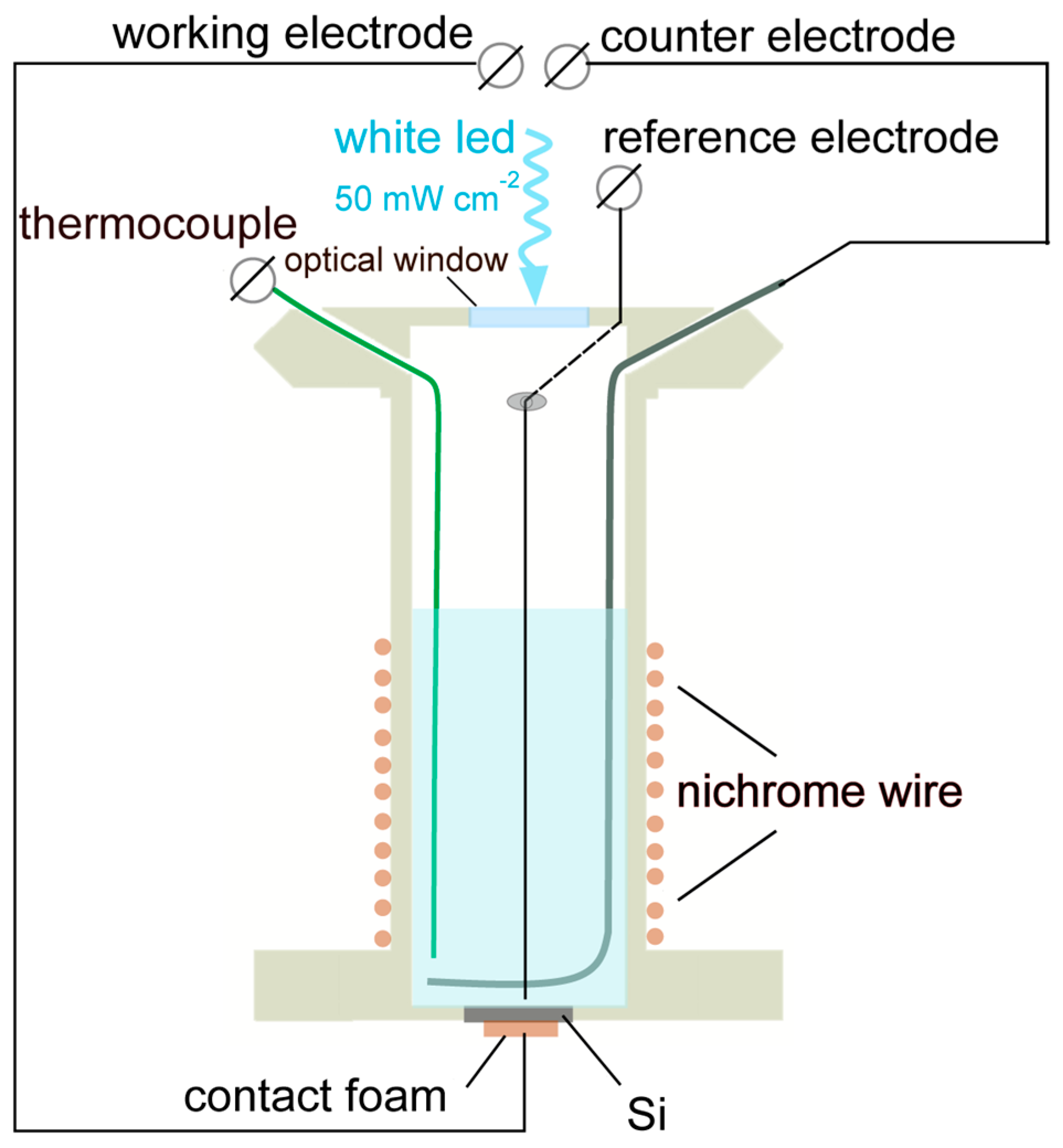
Figure 1 the shows configuration of the PEC cell used for the deposition experiments. The cell body was prepared from a tube (∅ 50 mm) of polyether ether ketone (PEEK from Rochling, Worms, Germany). The working electrodes have been mounted at the bottom of the cell. The electrode/electrolyte contact area was 0.5 cm
2. The back contact was prepared using highly conductive foam (Holland Shielding System BV, Dordrecht, The Netherlands). A Pt electrode was used as a reference, whose potential was determined with respect to a standard Ag/AgCl electrode (Redoxme AB, Norrköping, Sweden) and displayed with respect to a normal hydrogen electrode (NHE). The counter electrode was prepared from Pt in the form of a wire ring so that it did not shadow the working electrode. The electrodes were connected to a potentiostat (PARSTAT 2273 from Princeton Applied Research, Oak Ridge, TN, USA). The cell was supplied with the IL, which was composed of TMHA, TFSA (both from Solvionic, Toulouse, France), and 0.5 M or 1.0 M SiCl
4 (from VWR, Vienna, Austria). The total electrolyte volume was 8 mL. The electrolyte temperature was kept at 40 °C using a heating element made of nichrome (NiCr) wire wound around the cell body. The temperature was controlled by a thermocouple. A white LED illumination (4700 °K CCT) at intensity
N = 50 mW cm
−2 has been supplied to the working electrode through an optical window made of quartz.
The silicon substrates were prepared from a boron-doped <100> p-Si wafer with a resistivity of 10–30 Ω cm. The wafer surface was polished to a mirror-shiny appearance; its native oxide was removed in the solutions H2O2 + H2SO4 (1:1) and HF (1 HF:40 H2O). The p-GaAs electrode was prepared from <100> wafer doped with zinc (Zn) at a concentration of (1.2–1.8) × 1017 cm3. The AA2024 electrode was prepared from the alloy disc (∅ 14 mm); its surface was sequentially polished by 600, 1200, and 2500 grit sandpaper as well as with 3 μm and 1 μm diamond polishing paste with waterless polishing lubricant (Struers). The samples were ultrasonically cleaned in isopropyl alcohol for 15 min after each polishing step.
The deposition procedures were conducted in a glove box (M.Braun, Intergas-Systeme GMBH, Munchen, Germany) operating in a nitrogen atmosphere (N2, 0.5 ppm O2, and 0.5 ppm H2O). After deposition, the remaining electrolyte on the sample surface was removed in isopropyl alcohol (Merck KGaA, Darmstadt, Germany) at 40 °C. Afterward, the sample was dried using an argon stream (Elme Messer Lit, Vilnius, Lithuania) and kept in a hermetic container filled with argon.
The properties of the deposits were examined by the SEM Helios NanoLab 650 from FEI (Helios NanoLab 650, FEI, Hillsboro, OR, USA), equipped with an energy-dispersive X-ray spectrometer (EDX, Oxford Instruments, Abingdon, UK) INCAEnergy from Oxford Instruments. Cross-sections were prepared by a focused ion beam of Ga+ ions with an energy of 30 kV. A Pt layer has been sputtered on the sample to achieve interfacial stability during the cross-sectioning.
The structure of the surface layers was studied by grazing incidence X-ray diffraction (GI-XRD, SmartLab, Rigaku, Tokyo, Japan) using a SmartLab diffractometer from Rigaku with an X-ray tube equipped with a 9 kW Cu rotating anode.
Surface micro-topography has been studied using the optical profilometer Contour GT-K (Bruker Nano GmBH, Berlin, Germany) in white light interferometry (WLI) mode.
XPS analysis was performed on the Kratos Axis Supra spectrometer (Kratos AXIS Supra+, Manchester, UK) using monochromatic Al-Kα radiation (hν = 1486.7 eV) with an X-ray gun power of 225 W at 10−8 torr pressure and room temperature. The analyzed area at the sample center was approximately 0.16 mm2 in size, and high-resolution selected area scans were acquired using a pass energy of 20 eV. To compensate for sample charging during the measurement, a built-in charge neutralizer was used. The samples were also electrically isolated from the sample holder to avoid preferential charging effects. The binding energy scale of the recorded spectra was corrected by referencing the C 1s peak at 284.8 eV.
3. Results
First, we estimated the electrochemical windows of the IL electrolyte and that supplied with the Si precursor.
Figure 2a shows the cathodic curves obtained for the p-Si electrode in the electrolyte with and without Si precursor, which define the width of the windows. Significant enhancement of the cathodic process is obvious when 0.5 M precursor is added to IL.
The electrode is passive in the darkness–no appreciable current is observed (curve 1). Under illumination, a cathodic current starts in the precursor-free electrolyte at polarization Δ
E < −3.8 V (Δ
E means deviation from the open circuit potential
Eocp, curve 2,
Figure 2a). The current increases exponentially with polarization, denoting the electrochemical window of the electrolyte. A substantial current contribution is observed when the Si precursor is introduced: the photocurrent appears at ~−2.0 V and reaches ~1 mA cm
−2 at the potential where electrolyte decomposition begins (Δ
E = ~−3.8 V). In the subsequent potential region, the difference between the two curves remains approximately steady; the difference in the course of polarization does not change significantly. These data indicate the potentials at which silicon reduction is possible: SiCl
4 + 4e
− → Si.
Figure 3 characterizes the electrochemical system in terms of current variation under potentiostatic conditions. The measurements have been performed at Δ
E = −4.2 V, at which decomposition of IL is still sluggish (
Figure 2a). In the dark, the electrode is passive; the current flow is negligible. When illuminated, a current peak appears, and then the current drops to a steady-state value. Such behavior indicates a diffusion-limited process, which involves the transfer of the silicon precursor to the electrode surface. The limiting current also indicates a high conductivity of the illuminated electrode; no surface passivation is observed, which would be identified as a current decrease in the course of polarization. This is an important result in the view that pure silicon has a rather high resistance at room temperature, as the conductivity of pure silicon at room temperature is very low (4.3 × 10
−6 Ω
−1 cm
−1 at 300 K [
30]). A light-catalyzed process can be assumed, which is due to carriers’ generation in the deposit, thereby promoting the deposition process.
Figure 2b identifies the voltammetry that is characteristic of the p-GaAs electrode. The reduction process is demonstrated when the precursor’s concentration for the p-GaAs electrode is twice higher than the concentration for the p–Si electrode (1.0 M and 0.5 M, respectively). The more intense deposition results in a thicker coating on the GaAs, which slows down the cathodic process. This is evident from the curve maximum at Δ
E = ~−4.7 V and subsequent current decrease.
Figure 4 demonstrates the principal opportunity for PEC deposition of Si coating on a p–Si substrate. The deposition has been performed in a potentiodynamic mode at a scan rate of 10 mV s
−1, covering a wide potential region from the open circuit potential (
Eocp) to the polarization ∆
E = −5.0 V, where electrolyte decomposition is possible (
Figure 2a). SEM-EDS identified the deposition of a silicon-containing layer, which was about 270 nm thick (
Figure 4). The Si deposition began when the equilibrium potential
E0Si4+/Si was exceeded, and the process continued to rise with the negative potential shift. In the far polarization region, simultaneous decomposition of the electrolyte was possible; however, no carbon was detected in the deposit by the XPS (no C 1s peak). Carbon deposition under potentiostatic conditions will be discussed later.
The deposited sample contained some oxygen.
Figure 4b identifies the thickness of the oxygen-containing structure. The zone where the content of sputtered Pt drops down signifies the Pt/Si–O interface, and the zone where Si content reaches a limit signifies the thickness of the deposited layer. Note that some surface oxidation under ambient conditions is unavoidable. This is especially relevant in the case of thin layers. It is worth mentioning that the Si oxidation suggests an opportunity for electronic passivation as well as an improvement in antireflection performance due to interfacial light trapping. Porous silica (SiO
2) antireflective coatings prepared by the sol–gel process have been proposed. For instance, antireflection coatings based on SiO
2 nanocomposites have been reported to exhibit high levels of transparency, resistance to moisture, and antifogging properties [
31,
32].
Furthermore, we will focus on the deposition processes at high electrode polarization where electrolyte decomposition is possible (∆
E = −5.7 V,
Figure 5,
Figure 6 and
Figure 7).
Figure 5 shows the topographical data obtained for the profile of the deposited layer that extends over tens of micrometers. The surface roughness characterized by the top-to-valley distance (
z) is mostly less than 100 nm; in some areas, however, the distance can reach
z ~300 nm (indicated in blue). The topographical data in
Figure 5b demonstrates the surface features of the pristine p–Si substrate on which the layer was deposited. The surface is rather smooth; its roughness is much less than that of the deposited layer. The image identifies the greatest value of
z ~37 nm.
The SEM image in
Figure 6 shows the cross-section of the sample; it identifies the thickness of the deposited layer to be ~0.65 μm.
Th elemental composition of the deposited layer has been studied by EDS (
Figure 7). A significant amount of carbon (~18 at.%) was co-deposited with silicon. Carbon deposition was also confirmed by XPS. The 1s energy spectrum identified 19.9 at.% of the elemental carbon on the sample surface. A characteristic feature is that carbon is distributed within the silicon in the form of micrometer-sized inclusions (red or dark spots in
Figure 7). Note also that GI-XRD did not indicate any crystallinity features of the deposited layer, indicating its amorphous structure (
Supplementary Section).
A thin layer (~300 nm) of Si–C structure was deposited photoelectrochemically on the GaAs substrate as well (
Figure 8). GI-XRD did not indicate any crystallinity features of the layer.
A challenging goal is the creation of thin silicon films on technically important metallic substrates such as aluminum alloys, steel, or copper.
Figure 9 demonstrates a thin Si–C layer that was deposited on the aluminum–copper alloy AA 2024. The obtained layer was about 280 nm thick and contained 17 at.% of carbon. Note that a passive oxide layer is unavoidably present on the aluminum surface, which highly isolates the electrode with respect to the cathodic reaction. In IL, rather high polarizations can be applied so that the surface oxide can be decomposed, thereby making the electrode active. The deposit itself is also active under the influence of illumination (
Figure 10).
Figure 10 shows the current variation determined for the AA2024 coated with a Si–C layer under potentiostatic conditions. The current drop to a limiting value is characteristic of a diffusion-limited process. Substantial current growth is observed when the electrode is illuminated. Such behavior indicates a photoresponsible surface of the deposited silicon. The light-enhancing effect is also evident at higher polarization (∆
E = −4.5 V, curve 2), where electrolyte decomposition is significant (
Figure 2).
4. Discussion
Electrochemical deposition of Si layers is of great importance in numerous fields of application, such as photovoltaics, antireflection coatings, batteries, sensors, photoelectrodes for hydrogen and oxygen production from water, and the protection of metals from corrosion. Electrodeposition of silicon at room temperature is problematic due to the low electric conductivity of this element.
When illuminated, p-Si absorbs the photons, producing minority carriers (electrons). The photoelectrons are excited by the conduction band, and a space charge region is formed, which can extend up to 2000 Å into the silicon phase [
30,
33]. The Helmholtz layer can also form at the silicon/electrolyte interface [
30]. Under an open circuit, the electron-hole (e
−/h
+) pairs are generated so that holes arrive at the surface and charge it positively [
33] (p. 31). The illumination converts the electrode from an inactive to an active state, as
Figure 2 demonstrates. The negative polarization creates an electric field within the space charge region so that the photoelectrons can move to the electrolyte and participate in electrochemical reactions of the electrolyte decomposition or/and silicon reduction. When illumination is terminated, the carriers recombine, and the electrode becomes inactive (
Figure 2 and
Figure 3).
In the present investigation, we took advantage of p-type semiconductors to generate the photoelectrons and deposited photoelectrochemical Si as well as Si–C structures from IL on p-Si and p-GaAs substrates. We activated the semiconductors using white LED illumination and deposited the structures in the far region of cathodic potentials, where the decomposition of IL occurs. The deposition was achieved at nearly room temperature (40 °C).
Amorphous Si–C layers with micrometer-sized carbon inclusions in the silicon were formed. The produced layers were photo-responsive; the light-enhanced cathodic currents measured on an optically inactive electrode made of AA 2024 alloy proved this.
The proposed methodology paves the way for silicon modification by silicon-carbon structures. The proposed approach can also be applied to technically important alloys, as demonstrated by the deposition on the AA 2024 alloy. The deposition of Si structures on technically important alloys is important, first of all, for their anticorrosion protection.
We have demonstrated the principal opportunity to deposit thin-film silicon-based structures. There is a great margin to improve the quality of the layers and optimize the deposition conditions, such as cell configuration, kind of substrate, electrolysis parameters, precursor concentration, and temperature.
5. Patents
Patent application LT2023 519; No 107957; 19 May 2023.


 ,
, 