Article

Microstructure and Corrosion Behavior of the Modified Layers Grown In Situ by Plasma Nitriding Technology on the Surface of Zr Metal

1
Sino-French Institute of Nuclear Engineering and Technology, Sun Yat-Sen University, Zhuhai 519082, China
2
Science and Technology on Surface Physics and Chemistry Laboratory, Jiangyou 621700, China
*
Authors to whom correspondence should be addressed.
Coatings 2023, 13(7), 1160; https://doi.org/10.3390/coatings13071160
Submission received: 26 May 2023 / Revised: 19 June 2023 / Accepted: 21 June 2023 / Published: 27 June 2023
(This article belongs to the Section Ceramic Coatings and Engineering Technology)

Abstract

:
Preparing protecting coatings on the surface of Zr claddings has been regarded as one of the accident tolerant fuel (ATF) strategies. In this study, a series of nitride-modified layers were in situ grown by hollow cathode plasma nitriding on the surface of Zr metal. The influence of nitriding currents and time on the phases, composition, microstructure and corrosion resistance of the modified layers was investigated by X-ray diffraction (XRD), X-ray Photoemission Spectroscopy (XPS), transmission electron microscope (TEM), scanning electron microscopy (SEM) with energy dispersive spectrometer (EDS) and potentiodynamic polarization curves. The ZrO2 layer with loose microstructure and cracks prefers to form under low nitriding current of 0.4 A, which also causes poor corrosion resistance. The high temperature caused by high nitriding currents (0.6 A and 0.8 A) promote the formation of compact nanocrystalline layers, made up of nitride and oxynitride. Below the nanocrystalline layer, it is Zr2N caused by N penetration. Besides this, a double-layer structure of the nanocrystalline layer, i.e., an equiaxed crystal zone with a grain size of ~10–50 nm on the surface and a long strip grain region beneath it was observed. The compact nitride/oxynitride layer with excellent interface bonding can improve the corrosion resistance effectively.

1. Introduction

Zirconium alloy has been widely used as pressurized water reactor (PWR) nuclear fuel cladding material because of its low thermal neutron absorption cross section, good compatibility with uranium, excellent radiation resistance and mechanical properties [1,2]. Accident tolerant fuel (ATF) cladding materials have attracted a lot of attention due to the Loss of coolant accident (LOCA). Among all ATF strategies, preparation of a protecting coating (e.g., Cr, FeCrAl, HEAs, MAX, CrN, ZrN etc.) on the surface of zirconium alloy is one of the most popular [3]. Due to their high hardness, excellent friction, wear properties, good corrosion resistance and high thermal stability, transition metal nitrites, such as CrN, TiN and ZrN, have attracted extensive attention in the fields of protective coatings [4,5,6], biomaterial [7] and diffusion barrier layers [8]. Compared with TiN and other metal nitrides, ZrN shows better mechanical and frictional properties and oxidation resistance [9,10]. Of course, nanocrystalline ZrN film is also considered as an ATF coating due to its high irradiation resistance [11,12]. The preparation of ZrN coatings with compact structure and excellent interface bonding strength is essential to protect the zirconium alloy. In addition, under the normal operation condition, the research on corrosion resistance of ZrN protection layer is also important to ensure that the coating works [13].
So far, many methods have been used to prepare ZrN coatings, including magnetron sputtering [14,15], vacuum-arc deposition system [5], hollow cathode ion plating technology (HCD-IP) [16,17], ion beam sputtering [18,19,20] and so on. The previous studies have shown that the partial pressure of N2, substrate bias, deposition temperature and doped element can significantly affect the bonding strength between coating and matrix [21], the texture of ZrN coating [22], microstructure, density [23,24,25,26] and its mechanical properties, corrosion resistance, and oxidation resistance [27]. Of course, the preparation of the ZrN-modified layer by nitriding on the surface of the zirconium alloy has also been studied, including high-energy nitrogen ion implantation [25,28,29,30,31] and plasma nitriding [32,33,34]. Nimu Chand Reger et al. [32] used thermal nitriding of laser-processed Zr to improve its wear and corrosion properties. The nitriding temperature has a stronger influence on the microstructure, hardness and wear resistance of nitride layer than the nitriding time. The nitride layers, containing ZrN and ZrO2 as major phases and Zr2N and Zr7O8N4 as minor phases, can be used to increase the corrosion and wear resistance of Zr in physiological environment. Thermal treatment in nitrogen was also used to modify the surface of Zr-2.5Nb alloys under different temperatures (700–1200 °C). All of the modified specimens have better corrosion resistance, pitting resistance and friction wear than the substrate [34]. The corrosion inhibition behaviors of ZrNx thin films with varied N vacancy concentration (VN) were explored by Chenrui Pei et al. [35]. The ZrNx films with VN ≈ 0.3 have the highest inhibition efficiency because the donation of the valence band in ZrN0.67 is higher than that of other molecules. The inhibition efficiency or oxidation resistance increases with the decrease in teh overlapping range (EHOMO-ELUMO). The ZrN nanocrystalline coating prepared by double-cathode glow discharge plasma technique shows remarkable cavitation erosion resistance and has the potential for protecting alloys from cavitation erosion damage [36].
As mentioned earlier, PVD methods have been widely used to prepare ZrN coatings on the metal surface. However, the ZrN coatings prepared by PVD have some shortcomings, such as sharp interface, low crystalline and many defects in the coatings [19,37]. ZrN coatings prepared by single high-energy nitrogen ion implantation also have some disadvantages, such as uneven distribution of nitrogen ions and large number of defects generated by high-energy particle irradiation [38]. What is more, with the above two methods, it is difficult to process the workpiece with a complex structure. The high-energy ion implantation equipment is expensive, and industrial application is difficult to achieve. These shortcomings seriously limit the application of ZrN coatings in nuclear fuel cladding. Plasma nitriding technology has been widely used in aerospace, petrochemical, shipbuilding and other fields because of its advantages, such as surface treatment of workpieces with complex structure, high dose injection in a short time, low energy ion implantation with less damage and good bonding strength between modified layer and matrix [32,33]. In this paper, modified ZrN layers were grown on the surface of zirconium metal by the hollow cathode plasma nitriding method. The effects of nitriding currents and time on the microstructure, composition and electrochemical corrosion properties of modified layer were investigated.

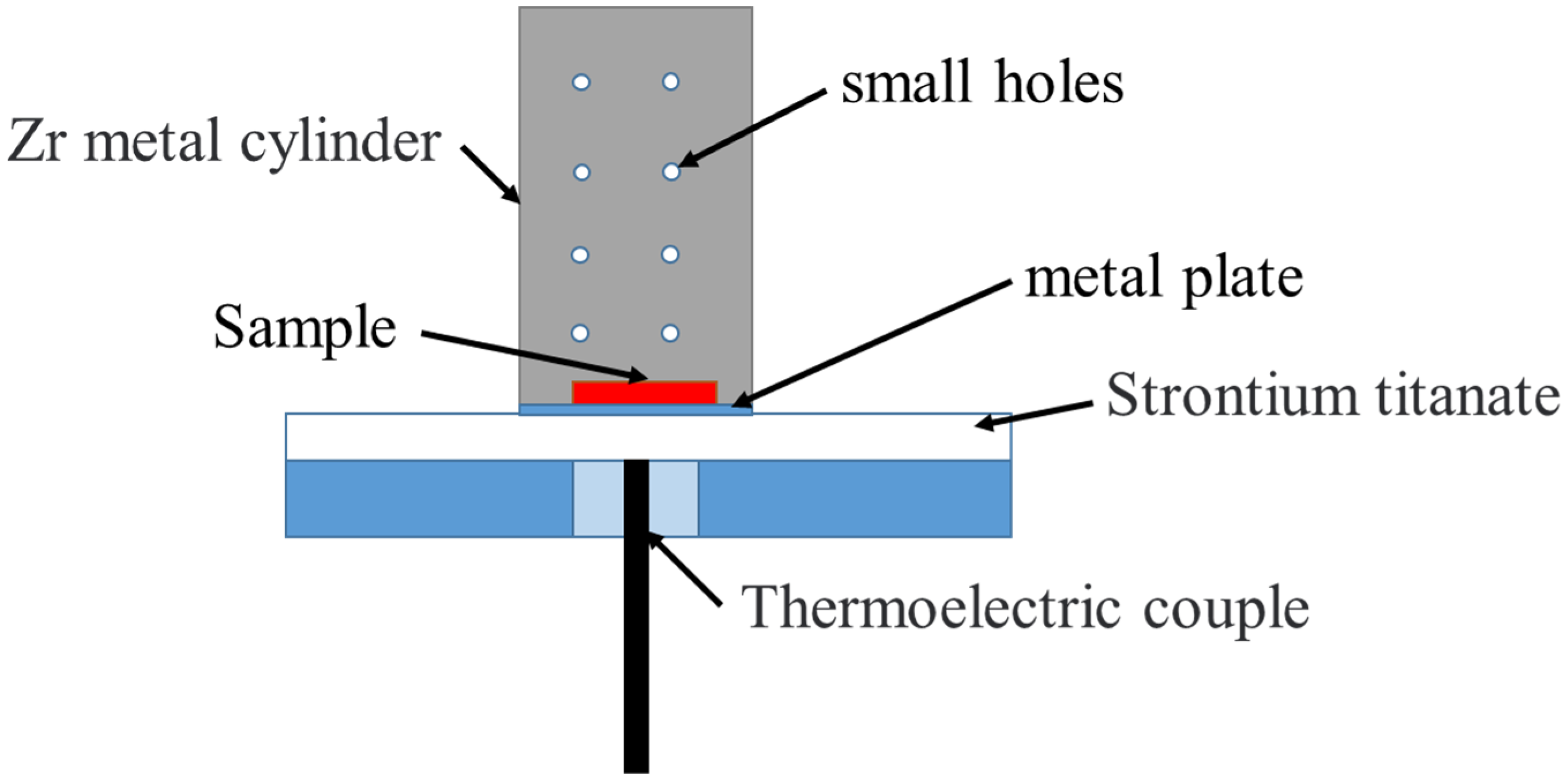
2. Materials and Methods

The zirconium metal with a purity of 99.9% was produced by Zhongnuo Advanced Material (Beijing, China) Technology Co., Ltd. Firstly, the samples were cut into a flat plate with a size of 10 × 10 × 0.5 mm by wire cutting. Next, both sides of the samples were polished with #500, #800, #1500, #2000 sandpaper successively to remove the surface oxide layer. Then, the surfaces of the samples were polished with a polishing agent with a particle size of 0.25 μm. Finally, the polished samples were cleaned by ultrasonic cleaning machine for 10 min in acetone, alcohol and deionized water in turn to remove particulate impurities and other organic pollutants from the zirconium surfaces.
The simplified schematic diagram of the plasma nitriding system used in this study is shown in Figure 1. The plasma generator is a cylindrical Zr metal cylinder connected with cathode, the upper end of which is sealed and the lower end is opened. Many small holes on the side of the cylinder were processed, which were used to introduce nitrogen into the metal cylinder. The samples were placed on a metal plate, and then the metal cylinder was inverted on the metal plate. Beneath the metal plate was a sheet of strontium titanate, under which a thermocouple was placed to detect the temperature during nitriding. Strontium titanate was used to insulate metal samples and thermoelectric couple. Before nitriding, the vacuum of the chamber was pumped to ~3.5 Pa by a mechanical pump. Then, nitrogen was injected into it for washing. This process was repeated five times to remove as many impurities as possible. Finally, nitrogen (purity 99.999%) with a flow of 90 SCCM was injected into the chamber until the pressure remained stable at ~200 Pa. Nitriding was carried out under a 900 V voltage. In this study, the nitriding currents and the nitriding time were changed to investigate their influence on the microstructure and corrosion resistance of the modified layers. The nitriding currents were regulated by the duty cycle. The nitriding currents increase with duty cycle when the voltage is fixed. The relevant experimental parameters are listed in Table 1.
X-ray diffraction (XRD, D/Max 2500V, Rigaku, Tokyo, Japan) was used to characterize the phase of the modified layers. The X-ray is Cu Kα (λ = 0.15418 nm). The conventional θ–2θ scanning from 25° to 60° was carried out with a scanning step of 0.02° and a scanning rate of 6°/min. The penetration depth of the N element was analyzed by the Zeiss field emission scanning electron microscope (SEM, Merlin, Carl Zeiss, Oberkochen, Germany) combing with Energy Dispersive Spectroscopy (EDS). The cross-sectional SEM samples were cut using a slow saw and cooled with a coolant. Then, the samples were cleaned by ultrasonic in acetone, alcohol and deionized water in turn. X-ray photoelectron spectroscopy (XPS, PHI 5300, PerkinElmer, Waltham, MA, USA) was performed to analyze the chemical composition and chemical states of the modified layers. X-ray source (Mg Kα, hν = 1253.6 eV) with a power of 150 W was used to excite the photoelectron. The size of the analyzed area was about ϕ 2–3 mm. During analysis, the base pressure was maintained below 5 × 10⁻⁸ torr, the electron emission angle was 54°; a charge neutralizer (5 eV/5 mA) was used. In addition, to realize the in-depth analysis of the elements in the modified layers, a 4 keV argon ion gun was used to sputter the surfaces of the samples for ~8–10 min to remove the surface contamination as much as possible. A focused ion beam (FIB, S9000X, Tescan, Brno, Czech Republic) was used to extract a TEM lamella from the surface of the modified layer. Then, the lamella was thinned by FIB milling steps to achieve electron transparency. The microstructure was characterized by JEOL 2100F transmission electron microscopy (TEM, JEOL 2100F, JOEL, Tokyo, Japan) with a 200 kV voltage. Electrochemical workstation was used to measure the potentiodynamic polarization curves of the modified samples at room temperature, with a Na2SO4 solution (0.1 M) as electrolyte. Platinum electrode with a size of 2 × 2 cm and a saturated calomel solution electrode were used as auxiliary electrode and opposite electrode, respectively. The samples were first soaked in the electrolyte until the open-circuit potential (OCP) was stable. The voltage variation range of the potentiodynamic polarization curve was OCP ± 100 mV and the scanning speed was 0.0005 V/s.

3. Results and Discussion

3.1. Influence of Nitriding Current on Temperature

During plasma nitriding, the bombardment of nitrogen plasma would transfer energy to the sample, resulting in the increase in sample temperature. The temperature can significantly affect the microstructure and performance of the modified layers [32,39,40]. Thus, it is important to obtain the temperatures during the nitriding process. Figure 2 shows the variation of nitriding temperatures with nitriding time under different nitriding currents of 0.4 A, 0.6 A and 0.8 A. As can be seen from the figure, the temperatures increased gradually with the increase in nitriding time and reached saturation when the nitriding time was about 25 min. The stable saturation temperature increased with the increase in nitriding current, with values of about 340 °C, 440 °C and 520 °C under currents of 0.4 A, 0.6 A and 0.8 A, respectively. It should be pointed out that a layer of strontium titanate sheet was between the samples and the thermocouple; thus, the actual temperatures of the nitriding samples should be higher than the measured values.

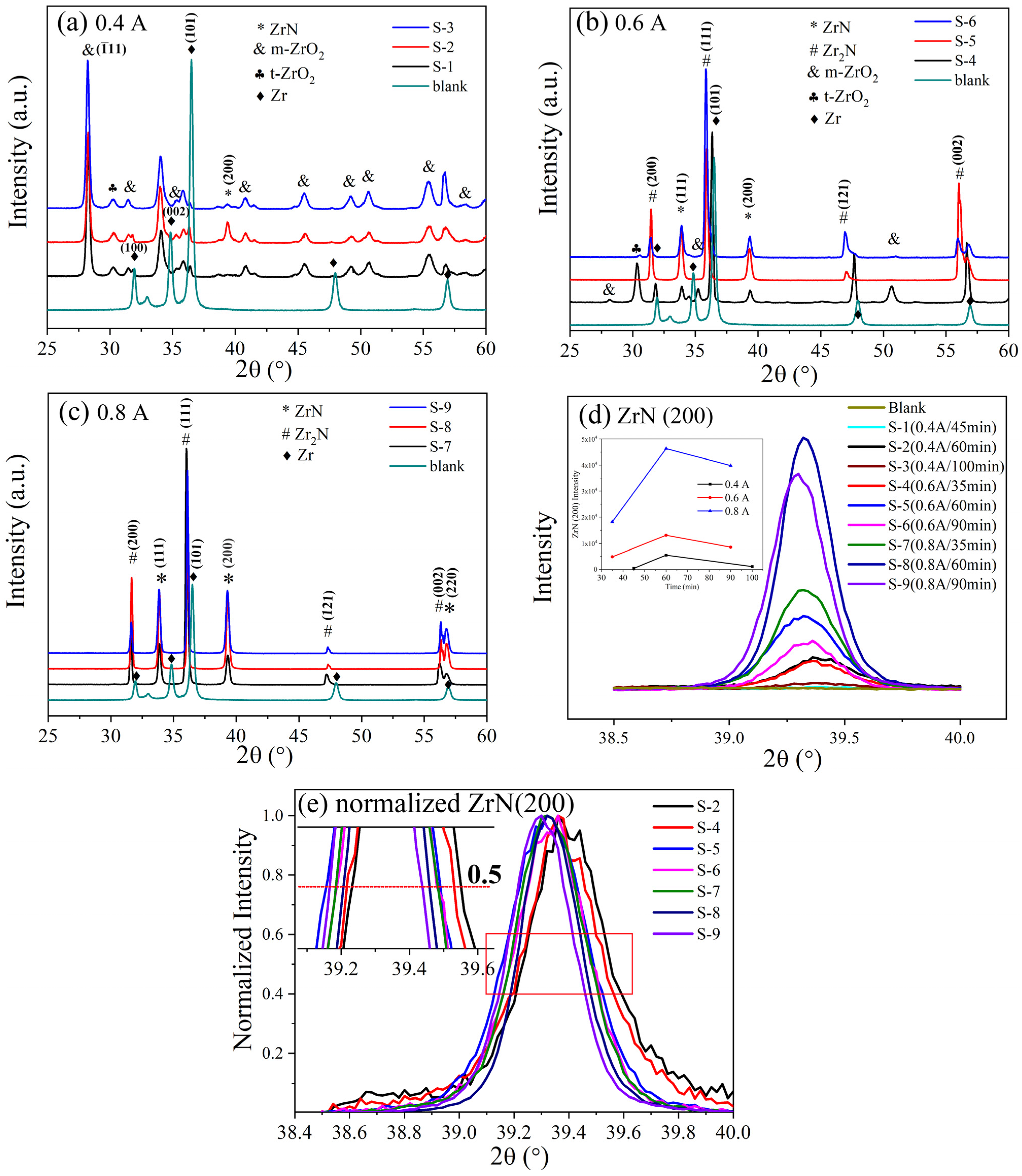
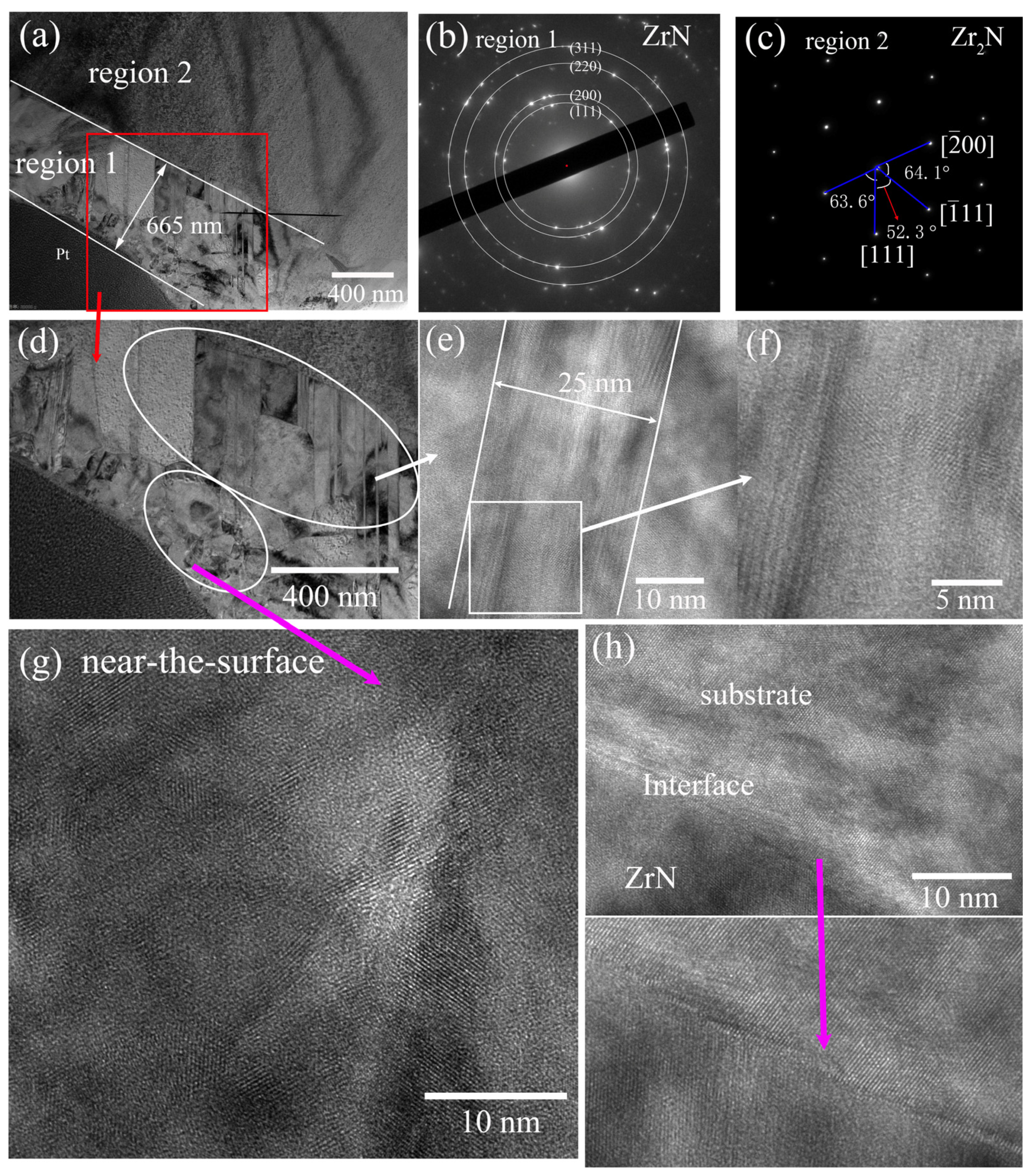
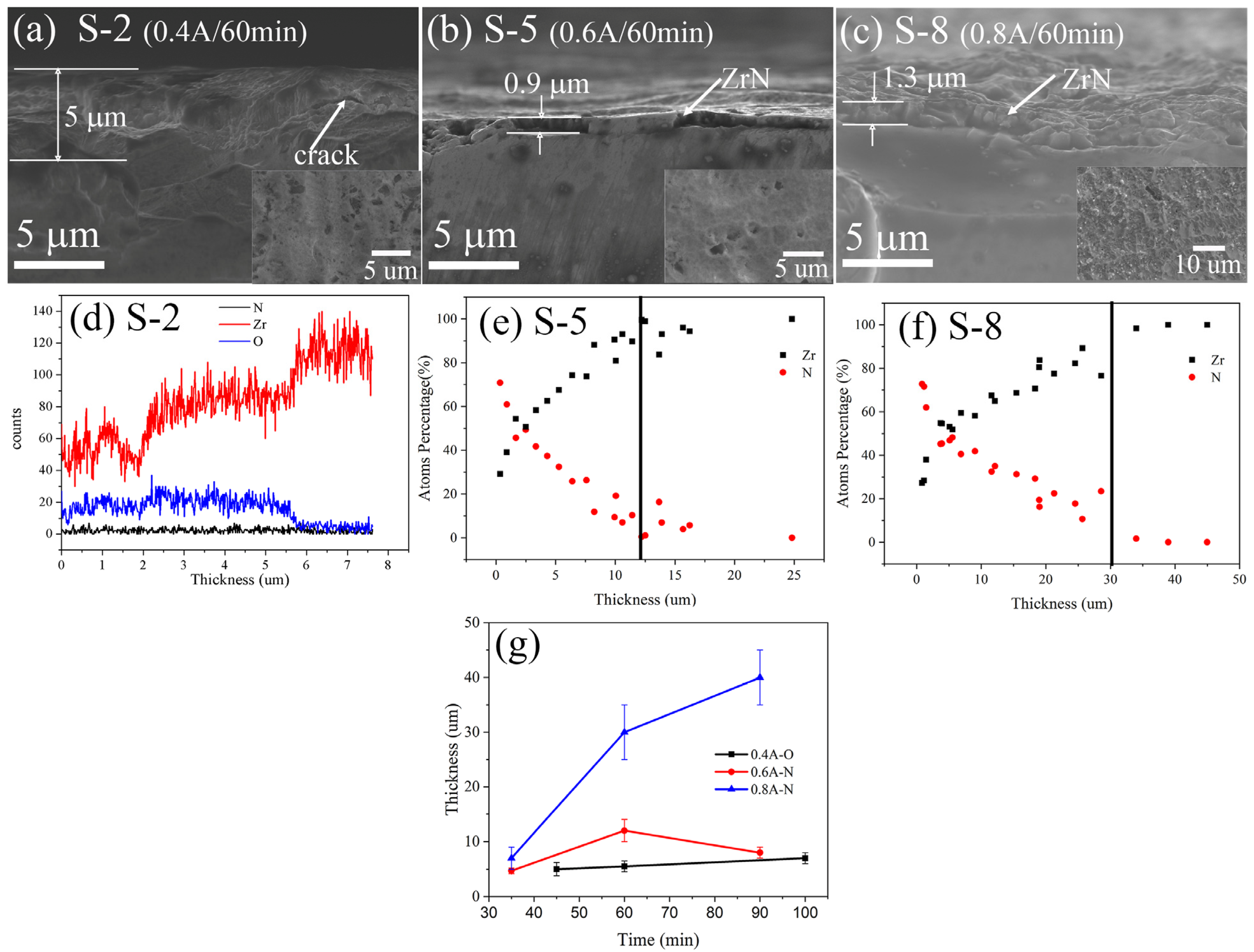
3.2. Phase, Composition and Microstructure

In order to characterize the phases of the modified layers, XRD patterns of the samples nitrided under different nitriding currents of 0.4 A, 0.6 A and 0.8 A were measured, as shown in Figure 3a–c, respectively. When the nitriding current was 0.4 A, ZrO2 formed significantly. Only a weak ZrN (200) diffraction peak at 39.4° appeared, indicating that only a small amount of ZrN generated in the modified layers. What is more, the ZrO2 was mainly in the monoclinic phase with a little tetragonal phase. With the nitriding current increasing to 0.6 A, the sample nitrided for 35 min (S-4) also had nonnegligible ZrO2, as shown in Figure 3b. Nevertheless, the peaks of ZrN (111) and (200) were more obvious than those of the samples prepared at 0.4 A, which meant more formation of ZrN. The peak positions of ZrN (111), (200) and (220) were 33.9° and 39.3°, 56.8°, respectively, which corresponded to the JCPDS file no. 02-0956 and the reports in [5,41]. In addition, the peaks at 31.6°, 35.9°, 47.3°and 56.3° were in agreement with the Zr2N peaks (JCPDS file no. 46-1204) and the results in the [41,42]. The ZrN (200) intensity under different nitriding conditions is shown in Figure 3d. The variation of ZrN (200) intensity with time was inserted in the upper left corner of Figure 3d. With the increase in nitriding time (S-5 and S-6), the diffraction peaks of ZrO2 and Zr substrate were no longer observed, and the relative intensity of ZrN (111) and (200) diffraction peaks became stronger. This indicated that the modified layers were mainly in the ZrN and Zr2N phases. When the nitriding current was 0.8 A, no ZrO2 was observed in the sample with the nitriding time of 35 min. Of cause, the relative intensity of ZrN (111) and (200) diffraction peaks further increased (as shown in Figure 3d); Zr2N was also observed. It can be concluded that the high nitriding current is beneficial for the formation of ZrN.
The residual oxygen or water vapor in the reaction chamber and the higher affinity of O2 towards Zr than N2 (ΔG = −118 Kcal/mol for ZrO2 and ΔG = −74 Kcal/mol for ZrN) [32] could be responsible for the formation of ZrO2 during nitriding. The high temperature due to the high nitriding current can increase the N2 binding ability [34] and promote the formation of ZrN. Therefore, more ZrO2 formed at 0.4 A with a low stable saturation temperature of ~340 °C, and nitride preferred to form at 0.6 A and 0.8 A with stable saturation temperatures of ~440 °C and ~520 °C, respectively. This result is also consistent with that of the previous report [32] that the ratio of nitrogen to oxygen in the films increases with nitriding duration and temperature. To investigate the influence of nitriding parameters on the grain size of ZrN, the normalized intensity of ZrN (200) peaks under different conditions is shown in Figure 3e. The edge values of the full width at half maximum (FWHM) were magnified and inserted in in the upper left corner of (e). It could be seen that the FWHM had no significant difference, indicating that the nitriding current, nitriding temperature and nitriding time had no significant influence on the grain size of ZrN.
XPS was used to analyze the composition of the modified layers, and the split-peak fitting was carried out. All of the spectroscopies were corrected with a 284.6 eV peak of the C element, as was performed in other works about ZrN [12,34,35,42]. Figure 4a–c present the Zr3d high resolution XPS of the samples prepared at 0.4 A/100 min, 0.6 A/60 min and 0.8 A/60 min, respectively. The corresponding XPS of N1s and O1s are shown in Figure 4d–i, respectively. The peaks in Figure 4a–c with binding energies of 179.4~179.8 eV, 180.8~181.2 eV and 182.2~182.4 eV in this study ascribed to Zr3d5/2 of ZrN, ZrNxOy and ZrO2, respectively. The peaks of N1s in Figure 4d–f at 397.2~397.9 eV and 398.8~399.3 eV were attributed to ZrN and ZrNxOy, respectively. This was consistent with the results of previous reports, namely that the binding energies of Zr3d5/2 in ZrN, ZrO2 and ZrNxOy were 179.2–180.3 eV [14,43,44,45], 181.9–182.3 eV [14,45,46] and 180.6 ± 0.4 eV [45], respectively, and the binding energies of N1s in ZrN and ZrNxOy were 397.3–397.6 eV [14,43,44] and 399~399.9 eV [43,44], respectively. The peak of O1s at ~531.6 eV shown in Figure 4g–i corresponded to that of Zr-O, higher than that of the O1s in ZrO2. As reported by Nimu Chand Reger et al. [32], the shift in the binding energies of O1s in the nitriding samples can be attributable to the incorporation nitrogen atoms. The peak of ~533.3 eV may result from the implantation and redeposition of oxygen atoms during sputtering or the residual oxygen. As pointed out by Grzegorz Greczynski et al. [47], implantation and redeposition of oxygen atoms during sputter etching is unavoidable. In addition, the high surface roughness of the samples in this study may also result in that the surface contaminants cannot be removed from some areas.
It could be seen from Figure 4a that the layer prepared at 0.4 A/100 min was mainly ZrO2, followed by ZrNxOy, and contained a small amount of ZrN. It was consistent with the results of a large amount of ZrO2 and very weak ZrN observed in the XRD pattern in Figure 3a. The Zr3d and N1s X-ray photoelectron spectra were almost the same for the layers prepared under 0.6 A/60 min and 0.8 A/60 min. No peak of Zr3d related to ZrO2 was observed, and the peak of ZrN increased significantly. Thus, the modified layers at 0.6 A/60 min and 0.8 A/60 min were mainly composed of ZrN and ZrNxOy. It could be concluded that the low temperature and low N plasma density at 0.4 A are beneficial for the formation of ZrO2, which is corresponding to the results of XRD in Figure 3. With the increase in the nitriding current, the higher temperature and N plasma density can promote the formation of ZrN. In addition, although only ZrN phase was found in the XRD pattern in Figure 3b,c, XPS results showed that the modified layer contained non-negligible zirconium nitrogen oxides.
To further investigate the microstructure of the modified layer after nitriding, the cross-sectional TEM images of the sample after a 0.6 A/60 min nitriding are shown in Figure 5. According to the TEM image, the nitriding sample was divided into two regions, a thin nanocrystalline layer (Region 1 between two white lines) with a thickness of ~665 nm on the surface and substrate (Region 2), as the depth increased. The bottom white line denoted the surface of the modified layer, and the top white line represented the interface between the nanocrystalline modified layer and the substrate (Region 2). To clarify the phase of the nanocrystalline layer, selected area electron diffraction (SAED) in Region 1 was performed, as shown in Figure 5b. The diffraction rings were consistent with the (111), (200), (220) and (311) crystal planes of ZrN. What is more, no other phase was observed obviously. Therefore, a nanocrystalline ZrN layer formed on the surface during the nitriding. Similarly, the SAED of Region 2 is shown in Figure 5c, which was identified to Zr2N. Combined with the result of XRD, it can be concluded that a Zr2N layer without changing the grain morphology of the Zr substrate formed beneath the nanocrystalline ZrN layer. In addition, a large number of defects similar to radiation damage defects generated in Region 2, as shown in Figure 5a.
Figure 5d is the local amplification image of Region 1. Obviously, the grain morphology of the nanocrystalline ZrN thin layer had different characteristics with the increase in depth, i.e., the surface was an equiaxed crystal zone with a grain size of ~10–50 nm. Beneath this zone was a long strip grain region w a typical characteristic of shear plastic deformation. Figure 5e shows the enlarged image of the grain boundary between the grains in the long strip grain region. Figure 5f is the HRTEM image of the grain boundary. It could be seen that there were a lot of dislocations in the grain boundary with a width of about 25 nm. In the process of nitriding, the penetration of interstitial N can lead to the expansion of lattice and produce high stress. With the increase of N, the Zr would transform to Zr2N and further ZrN. The high stress can also induce the plastic deformation of the modified layer. It can be inferred that this was the same as the grain refinement mechanism induced by plastic deformation during the SMA treatment [48]. The plastic deformation first forms dislocations within the original large grains. With the accumulation of dislocations, the dislocations transform into small angle grain boundaries, thus separating the original large grains into independent small grains, and then the subgrain boundaries transform into large angle grain boundaries so as to achieve grain refinement [48]. The near-the-surface view of the equiaxed crystal zone is shown in Figure 5g. A lot of nanocrystalline formed in this region. In addition, some amorphism was also observed. The interface between the ZrN layer and Zr2N was also studied by the local HRTEM image, as shown in Figure 5h. The image beneath it was the locally enlarged image of Figure 5h. An excellent bounding interface with partial grid between the ZrN layer and Zr2N could be seen. No disordered phase boundary was observed in the interface, but an ~5 nm interface with a large number of dislocations was seen.
SEM combined with EDS was used to study the cross-sectional microstructure and the N or O element penetration depth. Figure 6a–c are the cross-sectional SEM images of the representational samples of S-2 (0.4 A/60 min), S-5 (0.6 A/60 min) and S-8 (0.8 A/60 min), respectively. The inset images in the bottom right corner were the surface topographies of the corresponding modified layers, which showed that the modified layers were compact and had high surface roughness. The corresponding distributions of O or N and Zr are shown in Figure 6d–f, respectively. For the sample of S-2, there was a modified layer on the surface, which had a thickness of about 5 μm. Combined with the EDS in Figure 6d and the results of XRD and XPS above, it was confirmed that this layer was mainly composed of ZrO2. What is more, a loose structure and cracks could be seen in this layer. For the samples prepared at 0.6 A and 0.8 A, a compact modified layer on the surface, obviously different from the matrix, formed. According to Figure 5, this thin layer was identified as ZrN. The thicknesses of the ZrN layers for S-5 and S-8 were about 0.9 μm and 1.3 μm. The thickness of the ZrN layer increased with the increase in the nitriding current. The EDS results in Figure 6e,f showed that the N element penetration depths, ~12 μm for S-5 and ~30 μm for S-8, were far more than the thickness of ZrN, which was due to the formation of Zr2N beneath the ZrN layer. It should be noted that the line scanning of EDS is not sensitive to the N element, so point scanning at different depths was used to analyze the N distribution. Figure 6g is the variation of N or O penetration depths with nitriding time. The increase in nitriding current effectively increased the penetration depth of elements, which was mainly due to the fact that the higher nitriding current has a higher N or O plasma density and higher temperature. In addition, with the increase in nitriding time, the penetration depth also gradually increased, except for 0.6 A/60 min. As can be seen from Figure 2, the unexpectedness of 0.6 A/60 min could be interpreted as the slightly higher temperature than that of the other samples of 0.6 A.

3.3. Corrosion Resistance

Figure 7a is the potentiodynamic polarization curves of the Zirconium alloy after nitriding. The corrosion current density (Icorr) and corrosion potential (Ecorr) were fitted, as shown in Figure 7b. Compared with the blank sample, all the modified layers had higher Ecorr. In addition, the modified layers containing ZrO2 in Figure 3 (S-1, S-2, S-3 and S-4) had higher Ecorr than those containing only ZrN and ZrNxOy. Ecorr is a measure of the reaction thermodynamic. The higher the corrosion potential, the more difficult it is to start the corrosion reaction [34]. In other words, the most difficult to react is ZrO2, followed by ZrN, and then Zr. Icorr is a physical parameter reflecting the reaction kinetics. Low Icorr always means excellent corrosion resistance [34]. Compared to the modified layers prepared at 0.6 A and 0.8 A, the layers prepared at 0.4 A had a higher Icorr (worse corrosion resistance), which may be due to the loose structure of ZrO2 and the formation of cracks, as shown in Figure 6a. On the contrary, the modified layers prepared at 0.6 A and 0.8 A had better corrosion resistance due to the formation of compact nitride, as shown in Figure 6b,c. In this study, the compact modified ZrN layers prepared by hollow cathode nitriding under reasonable parameters on the surface of zirconium metal can effectively improve the corrosion resistance of zirconium metal. It was reported that the corrosion resistance of the ZrN protective film is comprehensively affected by its microstructure, density, stress state and interface bonding strength [23,49,50]. Thus, the excellent corrosion resistance may be attributed to its dense structure and the interface with excellent bonding [49,51,52]. Though the ZrO2 had a higher Ecorr, the loose structure of ZrO2 was lethal to the corrosion resistance.

4. Conclusions

In summary, hollow cathode plasma nitriding was used to grow in situ the modified nitride layers on Zr metal under different nitriding currents and time in this study. The influence of nitriding current and time on the phases, composition and microstructure of the modified layers was investigated. At a low current (0.4 A), a layer mainly containing ZrO2 forms due to the low nitriding temperature. Nevertheless, under the higher nitriding current (0.6 A and 0.8 A), a nanocrystalline ZrN layer forms on the surface, and underneath it is a layer of Zr2N with the same grain morphology as that of the Zr substrate. The surface nanocrystalline layer is divided into double layers, i.e., an equiaxed crystal zone with grain size of ~10–50 nm on the surface, and a long strip grain region beneath it. The formation of refined grains of the ZrN layer may be attributed to the plastic deformation caused by the high stress induced by the N penetration. The potentiodynamic polarization curves show that both the formation of ZrO2 and ZrN/ZrNxOy cause the increase in Ecorr, and the modified layers containing ZrO2 have higher Ecorr than the layers containing only nitride and oxynitride. In addition, the loose microstructure and cracks of the ZrO2 layers obtained at a low current of 0.4 A can be responsible for the high Icorr. The compact ZrN layers prepared at higher current have better corrosion resistance. Finally, under reasonable parameters, the compact modified zirconium nitride layer grown by hollow cathode nitriding in situ on the surface of zirconium metal can effectively improve the corrosion resistance of zirconium metal.

Author Contributions

Conceptualization, F.Z. and L.S.; methodology, F.Z.; software, Q.Z. and W.Z.; validation, Q.Z., K.Z. and W.Z.; formal analysis, Q.Z., K.Z. and W.Z.; investigation, F.Z.; resources, Y.H.; data curation, L.S.; writing—original draft preparation, F.Z.; writing—review and editing, X.M. and F.Z.; visualization, L.S.; supervision, X.M.; project administration, Y.H.; funding acquisition, Y.H. All authors have read and agreed to the published version of the manuscript.

Funding

This research was funded by the National Natural Science Foundation of China (grant No. U2032143), Guangdong Major Project of Basic and Applied Basic Research (2019B030302011), Subject development fund (No. XKFZ201702) and Guangdong Basic and Applied Basic Research Foundation (Nos. 2022A1515110266 and 2023A1515012504).

Institutional Review Board Statement

Not applicable.

Informed Consent Statement

Not applicable.

Data Availability Statement

All data included in this study are available upon request by contact with the corresponding author.

Conflicts of Interest

The authors declare no conflict of interest.

References

  1. Liao, J.; Xu, F.; Peng, Q.; Yang, Z.; Li, Z.; Qiu, S. Research on the existence and stability of interfacial tetragonal zirconia formed on zirconium alloys. J. Nucl. Mater. 2020, 528, 151846. [Google Scholar] [CrossRef]
  2. Zhang, B.; Jiang, H.; Chai, L.; Zhao, X.; Ma, P.; Zhang, R.; Wang, P. Assessment of microstructure, mechanical and tribological properties of Zr-4 alloy after pre-oxidation and ion irradiation. Appl. Surf. Sci. 2023, 610, 155444. [Google Scholar] [CrossRef]
  3. Terrani, K.A. Accident tolerant fuel cladding development: Promise, status, and challenges. J. Nucl. Mater. 2018, 501, 13–30. [Google Scholar] [CrossRef]
  4. Purandare, Y.P.; Ehiasarian, A.P.; Hovsepian, P.E. Structure and properties of ZrN coatings deposited by high power impulse magnetron sputtering technology. J. Vac. Sci. Technol. A Vac. Surf. Film. 2011, 29, 011004. [Google Scholar] [CrossRef]
  5. Maksakova, O.V.; Webster, R.F.; Tilley, R.D.; Ivashchenko, V.I.; Postolnyi, B.O.; Bondar, O.V.; Takeda, Y.; Rogoz, V.M.; Sakenova, R.E.; Zukowski, P.V.; et al. Nanoscale architecture of (CrN/ZrN)/(Cr/Zr) nanocomposite coatings: Microstructure, composition, mechanical properties and first-principles calculations. J. Alloys Compd. 2020, 831, 154808. [Google Scholar] [CrossRef]
  6. Pogrebnjak, A.; Sobol’, O.V.; Beresnev, V.M.; Pshyk, O. Phase Composition, Thermal Stability, Physical and Mechanical Properties of Superhard on Base Zr-Ti-Si-N Nanocomposite Coatings. Ceram. Eng. Sci. Proc. 2010, 31, 127–138. [Google Scholar] [CrossRef]
  7. Xin, Y.; Liu, C.; Huo, K.; Tang, G.; Tian, X.; Chu, P.K. Corrosion behavior of ZrN/Zr coated biomedical AZ91 magnesium alloy. Surf. Coat. Technol. 2009, 203, 2554–2557. [Google Scholar] [CrossRef]
  8. Wang, Y.; Zhao, C.-h.; Cao, F.; Yang, D.-w. Barrier capability of Zr–N films with different density and crystalline structure in Cu/Si contact systems. Mater. Lett. 2008, 62, 3761–3763. [Google Scholar] [CrossRef]
  9. Spillmann, H.; Willmott, P.R.; Morstein, M.; Uggowitzer, P.J. ZrN, ZrxAlyN and ZrxGayN thin films—Novel materials for hard coatings grown using pulsed laser deposition. Appl. Phys. A 2014, 73, 441–450. [Google Scholar] [CrossRef]
  10. Qi, Z.B.; Wu, Z.T.; Liang, H.F.; Zhang, D.F.; Wang, J.H.; Wang, Z.C. In situ and ex situ studies of microstructure evolution during high-temperature oxidation of ZrN hard coating. Scr. Mater. 2015, 97, 9–12. [Google Scholar] [CrossRef]
  11. Egeland, G.W.; Wheeler, K.; Peralta, P.; McClellan, K.J.; Maloy, S.A.; Bond, G.M. Plastic deformation in zirconium nitride observed by nanoindentation and TEM. J. Nucl. Mater. 2011, 416, 253–261. [Google Scholar] [CrossRef]
  12. Craciun, D.; Vasile, B.S.; Lambers, E.; Makino, H.; Craciun, V. Microstructural investigations of 800 keV Ar ions irradiated nanocrystalline ZrN thin films. Surf. Eng. 2019, 36, 326–333. [Google Scholar] [CrossRef]
  13. Kim, W.; Jung, K.S.; Choi, B.H.; Kwon, H.S.; Lee, N.J.; Han, J.G.; Guseva, M.I.; Atamanov, M.V. Corrosion behavior of nitrogen-implanted Zircaloy. Surf. Coat. Technol. 1995, 76–77, 595–599. [Google Scholar] [CrossRef]
  14. Singh, A.; Kuppusami, P.; Khan, S.; Sudha, C.; Thirumurugesan, R.; Ramaseshan, R.; Divakar, R.; Mohandas, E.; Dash, S. Influence of nitrogen flow rate on microstructural and nanomechanical properties of Zr–N thin films prepared by pulsed DC magnetron sputtering. Appl. Surf. Sci. 2013, 280, 117–123. [Google Scholar] [CrossRef]
  15. Benia, H.M.; Guemmaz, M.; Schmerber, G.; Mosser, A.; Parlebas, J.-C. Investigation on non-stoichiometric zirconium nitrides. Appl. Surf. Sci. 2002, 200, 231–238. [Google Scholar] [CrossRef]
  16. Chou, W.-J.; Yu, G.-P.; Huang, J.-H. Bias effect of ion-plated zirconium nitride film on Si(100). Thin Solid Film. 2002, 405, 162–169. [Google Scholar] [CrossRef]
  17. Huang, J.-H.; Yang, H.-C.; Guo, X.-J.; Yu, G.-P. Effect of film thickness on the structure and properties of nanocrystalline ZrN thin films produced by ion plating. Surf. Coat. Technol. 2005, 195, 204–213. [Google Scholar] [CrossRef]
  18. Larijani, M.M.; Norouzian, S.; Afzalzadeh, R.; Balashabadi, P.; Dibaji, H. Effects of post annealing on micro and nanostructural properties of ZrN films prepared by ion beam sputtering technique on SS304. Surf. Coat. Technol. 2009, 203, 2486–2489. [Google Scholar] [CrossRef]
  19. Zhu, F.; Zhu, K.; Hu, Y.; Ling, Y.; Wang, D.; Peng, H.; Xie, Z.; Yang, R.; Zhang, Z. Microstructure and Young’s modulus of ZrN thin film prepared by dual ion beam sputtering deposition. Surf. Coat. Technol. 2019, 374, 997–1005. [Google Scholar] [CrossRef]
  20. Larijani, M.M.; Tabrizi, N.; Norouzian, S.; Jafari, A.; Lahouti, S.; Haj Hosseini, H.; Afshari, N. Structural and mechanical properties of ZrN films prepared by ion beam sputtering with varying N2/Ar ratio and substrate temperature. Vacuum 2006, 81, 550–555. [Google Scholar] [CrossRef]
  21. Kiahosseini, S.R.; Mojtahedzadeh Larijani, M. Effects of nitrogen gas ratio on the structural and corrosion properties of ZrN thin films grown on biodegradable magnesium alloy by ion-beam sputtering. Appl. Phys. A 2017, 123, 759. [Google Scholar] [CrossRef]
  22. Larijani, M.M.; Elmi, M.; Yari, M.; Ghoranneviss, M.; Balashabadi, P.; Shokouhy, A. Nitrogen effect on corrosion resistance of ion beam sputtered nanocrystalline zirconium nitride films. Surf. Coat. Technol. 2009, 203, 2591–2594. [Google Scholar] [CrossRef]
  23. Menghani, J.; Pai, K.B.; Totlani, M.K. Corrosion and wear behaviour of ZrN thin films. Tribol.—Mater. Surf. Interfaces 2013, 5, 122–128. [Google Scholar] [CrossRef]
  24. Huang, J.-H.; Hsu, C.-Y.; Chen, S.-S.; Yu, G.-P. Effect of substrate bias on the structure and properties of ion-plated ZrN on Si and stainless steel substrates. Mater. Chem. Phys. 2002, 77, 14–21. [Google Scholar] [CrossRef]
  25. Kavitha, A.; Subramanian, N.S.; Loganathan, S.; Kannan, R. Deposition and characterization of zirconium nitride (ZrN) thin films by reactive magnetron sputtering with linear gas ion source and bias voltage. In AIP Conference Proceedings; American Institute of Physics: College Park, MD, USA, 2014; pp. 1705–1707. [Google Scholar]
  26. Ju, H.; Yu, D.; Yu, L.; Ding, N.; Xu, J.; Zhang, X.; Zheng, Y.; Yang, L.; He, X. The influence of Ag contents on the microstructure, mechanical and tribological properties of ZrN-Ag films. Vacuum 2018, 148, 54–61. [Google Scholar] [CrossRef]
  27. Zhou, Q.G.; Bai, X.D.; Xue, X.Y.; Ling, Y.H.; Chen, X.W.; Xu, J.; Wang, D.R. The influence of Y ion implantation on the oxidation behaviour of ZrN coating. Vacuum 2004, 76, 517–521. [Google Scholar] [CrossRef]
  28. Liu, Y.Z.; Zu, X.T.; Qiu, S.Y.; Li, C.; Ma, W.G.; Huang, X.Q. Surface characteristics and oxidation behavior of nitrogen ion-implanted Zr–Sn–Nb alloy. Surf. Coat. Technol. 2006, 200, 5631–5635. [Google Scholar] [CrossRef]
  29. Han, J.G.; Lee, J.S.; Choi, B.H.; Kim, W.; Tang, G. Wear and fretting wear behaviour of ion-implanted Zircaloy-4. Surf. Coat. Technol. 1996, 83, 307–312. [Google Scholar] [CrossRef]
  30. Han, J.G.; Lee, J.S.; Kim, W.; Sun, D.S.; Chung, K.H. Zirconium oxide formation and surface hardening behavior by nitrogen implantation under oxygen atmosphere in Zircaloy-4. Surf. Coat. Technol. 1997, 97, 492–498. [Google Scholar] [CrossRef]
  31. Han, J.G.; Choi, B.H.; Kim, W.; Guseva, M. Tribological hard layer synthesis by duplex ion beam treatment. Nucl. Instrum. Methods Phys. Res. B 1997, 121, 79–83. [Google Scholar] [CrossRef]
  32. Reger, N.C.; Balla, V.K.; Das, M.; Bhargava, A.K. Wear and corrosion properties of in-situ grown zirconium nitride layers for implant applications. Surf. Coat. Technol. 2018, 334, 357–364. [Google Scholar] [CrossRef]
  33. Liu, Y.; Yang, Y.; Dong, D.; Wang, J.; Zhou, L. Improving wear resistance of Zr-2.5Nb alloy by formation of microtextured nitride layer produced via laser surface texturing/plasma nitriding technology. Surf. Interfaces 2020, 20, 100638. [Google Scholar] [CrossRef]
  34. Xia, C.; Liu, Q.; Song, T.; Chen, B.; Liu, S.; Li, Q. Corrosion behavior and wear resistance of Zr-2.5Nb alloy after thermal oxy-nitriding treatment. Surf. Coat. Technol. 2022, 446, 128756. [Google Scholar] [CrossRef]
  35. Pei, C.; Deng, L.; Liu, H.; He, Z.; Xiang, C.; Zhang, S.; Sun, D. Corrosion inhibition behaviors of ZrNx thin films with varied N vacancy concentration. Vacuum 2019, 162, 28–38. [Google Scholar] [CrossRef]
  36. Zhang, Y.; Xu, J.; Cheng, L.; Zhao, Y.; Peng, S.; Jiang, S. Exploring cavitation erosion resistance of ZrN nanocrystalline coating prepared by double-cathode glow discharge plasma technique. Vacuum 2020, 182, 109697. [Google Scholar] [CrossRef]
  37. Ghemras, I.; Abdelli-Messaci, S.; Alili, B.; González-Elipe, A.R.; Rico, V.J.; Izerrouken, M.; Khereddine, A.Y.; Hadj-Larbi, F. Characterizing the physicochemical and mechanical properties of ZrN thin films deposited on Zr substrates by pulsed laser technique. Eur. Phys. J. Appl. Phys. 2021, 95, 10301. [Google Scholar] [CrossRef]
  38. Liu, Y.Z.; Zu, X.T.; Zhu, S.; Wang, L.M. Phase formation and corrosion behavior of nitrogen implanted Zr–Sn–Nb alloy in alkaline environment. Nucl. Instrum. Methods Phys. Res. Sect. B Beam Interact. Mater. At. 2006, 246, 345–350. [Google Scholar] [CrossRef]
  39. Lee, S.J.; Kwon, H.S.; Kim, W.; Choi, B.H. Effects of compositional and structural change on the corrosion behaviour of nitrogen implanted Zircaloy-4. Mater. Sci. Eng. A 1999, 263, 23–31. [Google Scholar] [CrossRef]
  40. Tang, G.; Choi, B.H.; Kim, W.; Jung, K.-S.; Kwon, H.S.; Lee, S.J.; Lee, J.H.; Song, T.Y.; Shon, D.H.; Han, J.G. The characteristics of surface oxidation and corrosion resistance of nitrogen implanted zircaloy-4. Surf. Coat. Technol. 1997, 89, 252–257. [Google Scholar] [CrossRef]
  41. Khan, I.A.; Hassan, M.; Ahmad, R.; Qayyum, A.; Murtaza, G.; Zakaullah, M.; Rawat, R.S. Nitridation of zirconium using energetic ions from plasma focus device. Thin Solid Film. 2008, 516, 8255–8263. [Google Scholar] [CrossRef]
  42. Zheng, Y.; Li, X.; Liu, Y.; Sun, W.; Dong, C. Preparation and characterization of CuN-based ternary alloy films using Cr or Zr for stabilizing N. J. Mater. Res. 2017, 32, 1333–1342. [Google Scholar] [CrossRef]
  43. Roman, D.; Bernardi, J.; Amorim, C.L.G.d.; de Souza, F.S.; Spinelli, A.; Giacomelli, C.; Figueroa, C.A.; Baumvol, I.J.R.; Basso, R.L.O. Effect of deposition temperature on microstructure and corrosion resistance of ZrN thin films deposited by DC reactive magnetron sputtering. Mater. Chem. Phys. 2011, 130, 147–153. [Google Scholar] [CrossRef]
  44. Han, K.-C.; Lin, G.-Q.; Dong, C.; Tai, K.-P.; Jiang, X. Influence of Nitrogen Vacancy Concentration on Mechanical and Electrical Properties of Rocksalt Zirconium Nitride Films. Acta Metall. Sin. (Engl. Lett.) 2017, 30, 1100–1108. [Google Scholar] [CrossRef] [Green Version]
  45. Matsuoka, M.; Isotani, S.; Sucasaire, W.; Kuratani, N.; Ogata, K. X-ray photoelectron spectroscopy analysis of zirconium nitride-like films prepared on Si(100) substrates by ion beam assisted deposition. Surf. Coat. Technol. 2008, 202, 3129–3135. [Google Scholar] [CrossRef]
  46. Ning, S.; Zhang, Z. Phase-dependent and defect-driven d0 ferromagnetism in undoped ZrO2 thin films. RSC Adv. 2015, 5, 3636–3641. [Google Scholar] [CrossRef]
  47. Baer, D.R.; Artyushkova, K.; Brundle, C.R.; Castle, J.E.; Engelhard, M.H.; Gaskell, K.J.; Grant, J.T.; Haasch, R.T.; Linford, M.R.; Powell, C.J.; et al. Practical Guides for X-ray Photoelectron Spectroscopy (XPS): First Steps in planning, conducting and reporting XPS measurements. J. Vac. Sci. Technol. A 2019, 37, 031401. [Google Scholar] [CrossRef]
  48. Tao, N.R.; Wang, Z.B.; Tong, W.P.; Sui, M.L.; Lu, J.; Lu, K. An investigation of surface nanocrystallization mechanism in Fe induced by surface mechanical attrition treatment. Acta Mater. 2002, 50, 4603–4616. [Google Scholar] [CrossRef]
  49. Subramanian, B.; Swaminathan, V.; Jayachandran, M. Microstructural, tribological and electrochemical corrosion studies on reactive DC magnetron sputtered zirconium nitride films with Zr interlayer on steel. Met. Mater. Int. 2012, 18, 957–964. [Google Scholar] [CrossRef]
  50. Feng, L.; Xingsheng, S.; Zhaoxing, M.Y. Microstructure, Hardness and Corrosion Resistance of ZrN Films Prepared by Inductively Coupled Plasma Enhanced RF Magnetron Sputtering. Plasma Sci. Technol. 2008, 10, 170–175. [Google Scholar] [CrossRef]
  51. Yi, P.; Zhu, L.; Dong, C.; Xiao, K. Corrosion and interfacial contact resistance of 316L stainless steel coated with magnetron sputtered ZrN and TiN in the simulated cathodic environment of a proton-exchange membrane fuel cell. Surf. Coat. Technol. 2019, 363, 198–202. [Google Scholar] [CrossRef]
  52. Ningshen, S.; Gupta, R.K.; Kamal, S.; Chawla, V.; Chandra, R.; Mudali, U.K. Corrosion study of ZrN deposited on 304L stainless steel. Surf. Eng. 2013, 29, 264–270. [Google Scholar] [CrossRef]
Figure 1. Simplified schematic diagram of plasma nitriding.
Coatings 13 01160 g001
Figure 2. Variation of temperatures with nitriding time under different nitriding currents.
Coatings 13 01160 g002
Figure 3. XRD patterns of modified layer at different nitriding currents (a) 0.4 A, (b) 0.6 A and (c) 0.8 A, (d) detail view and (e) normalized intensity of ZrN (200). The inserted image in the upper left corner of (d) is the variation of intensity of ZrN (200) peak with nitriding time. The inserted image in the upper left corner of (e) is the locally enlarged image of the normalized (200) peak of ZrN (the red dotted line is the half height).
Coatings 13 01160 g003
Figure 4. (ac) Zr3d, (df) N1s, (gi) O1s X-ray photoelectron spectra of S-3 (0.4 A/100 min), S-5 (0.6 A/60 min) and S-8 (0.8 A/60 min). Blue, pink and cyan line represent the peak from ZrN, ZrNxOy and ZrO2, respectively.
Coatings 13 01160 g004
Figure 5. (a) Cross-sectional TEM images of the nitriding sample under 0.6 A/60 min, SAED of (b) Region 1 (nanocrystalline modified ZrN layer) and (c) Region 2 (Zr2N), (d) local amplification image of Region 1 nanocrystalline modified ZrN layer, (e) enlarged image and (f) HRTEM image of the grain boundary between the long strip grains in ZrN layer, HRTEM images of (g) the near surface region and (h) the interface between nanocrystalline modified ZrN layer and Zr2N.
Coatings 13 01160 g005
Figure 6. The cross-sectional SEM images and the corresponding depth distribution of N, Zr, O of (a,d) S-2 (0.4 A/60 min), (b,e) S-5 (0.6 A/60 min) and (c,f) S-8 (0.8 A/60 min). (g) Diffusion depth of O for samples prepared at current of 0.4 A and N for 0.6 A and 0.8 A. The inset images in the bottom right corner of (ac) are the corresponding surface topographies.
Coatings 13 01160 g006
Figure 7. (a) Potentiodynamic polarization curves, (b) corrosion current density (Icorr) and corrosion potential (Ecorr) for the Zirconium alloy after nitriding under different parameters.
Coatings 13 01160 g007
Table 1. The number of samples, nitriding currents, time and duty cycle.
Number of SamplesNitriding Current (A)Nitriding Time (min)Duty Cycle (%)
S-10.445~20
S-20.460~21
S-30.4100~21
S-40.635~25
S-50.660~36
S-60.690~27
S-70.835~43
S-80.860~44
S-90.890~43
Disclaimer/Publisher’s Note: The statements, opinions and data contained in all publications are solely those of the individual author(s) and contributor(s) and not of MDPI and/or the editor(s). MDPI and/or the editor(s) disclaim responsibility for any injury to people or property resulting from any ideas, methods, instructions or products referred to in the content.

