
Optical Trapping and Manipulation of Nanoparticles on Plasmonic Silicon-Nanostructured Array Coating on Silicon Film

 and
and 
Abstract
:1. Introduction
2. Model and Method
2.1. Method of Multipole Decomposition
2.2. Maxwell Stress Tensor Method
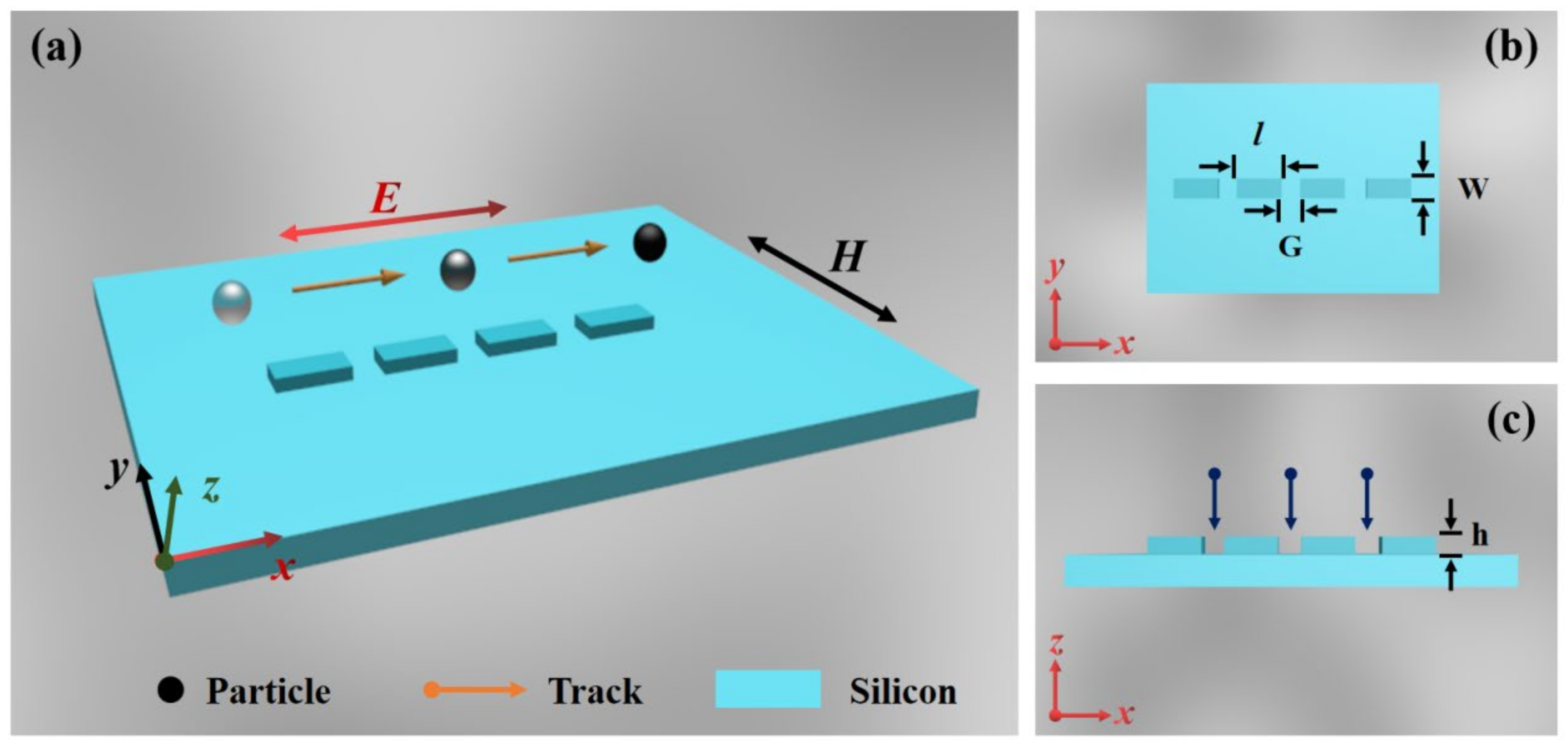
2.3. Structure and Modeling
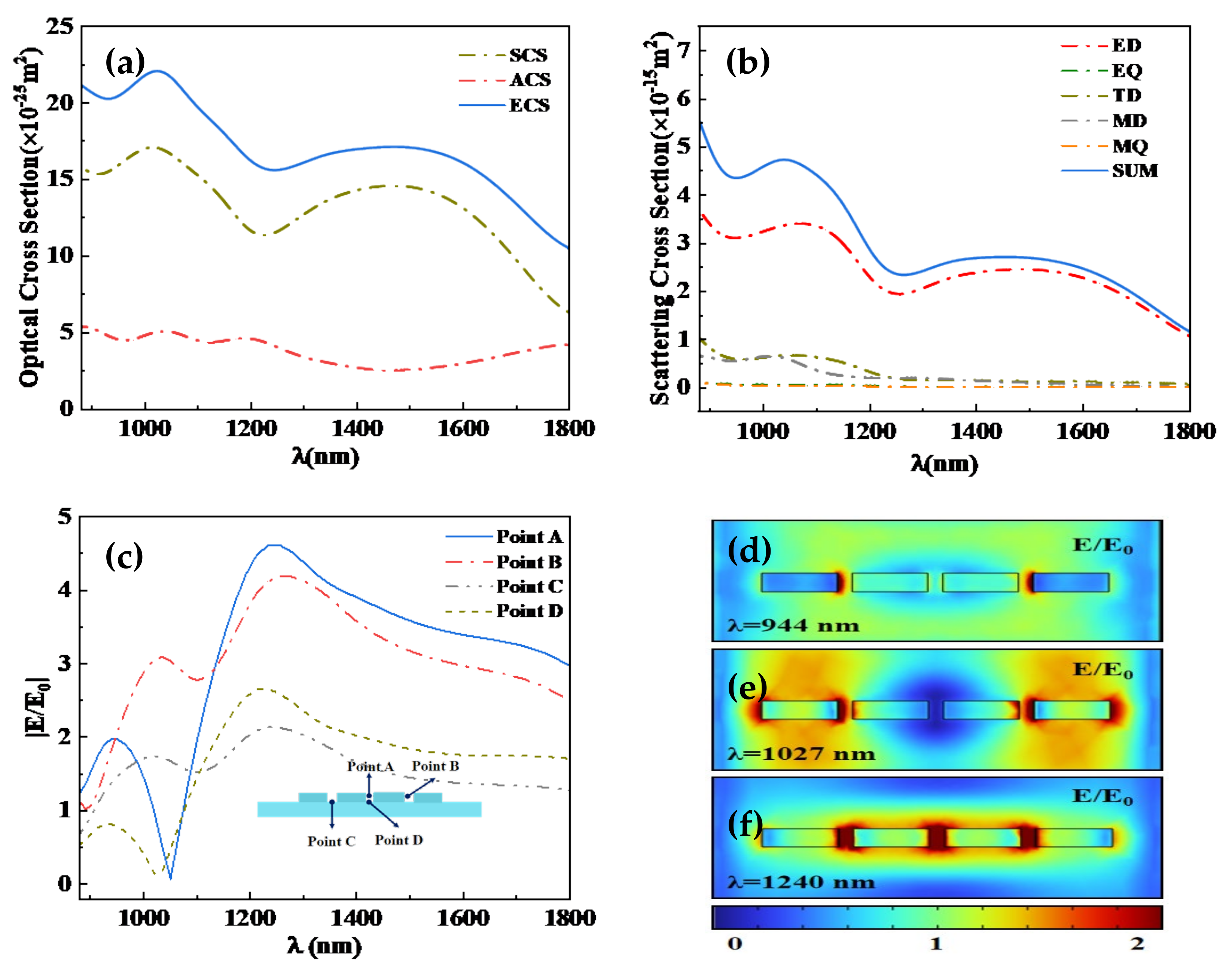
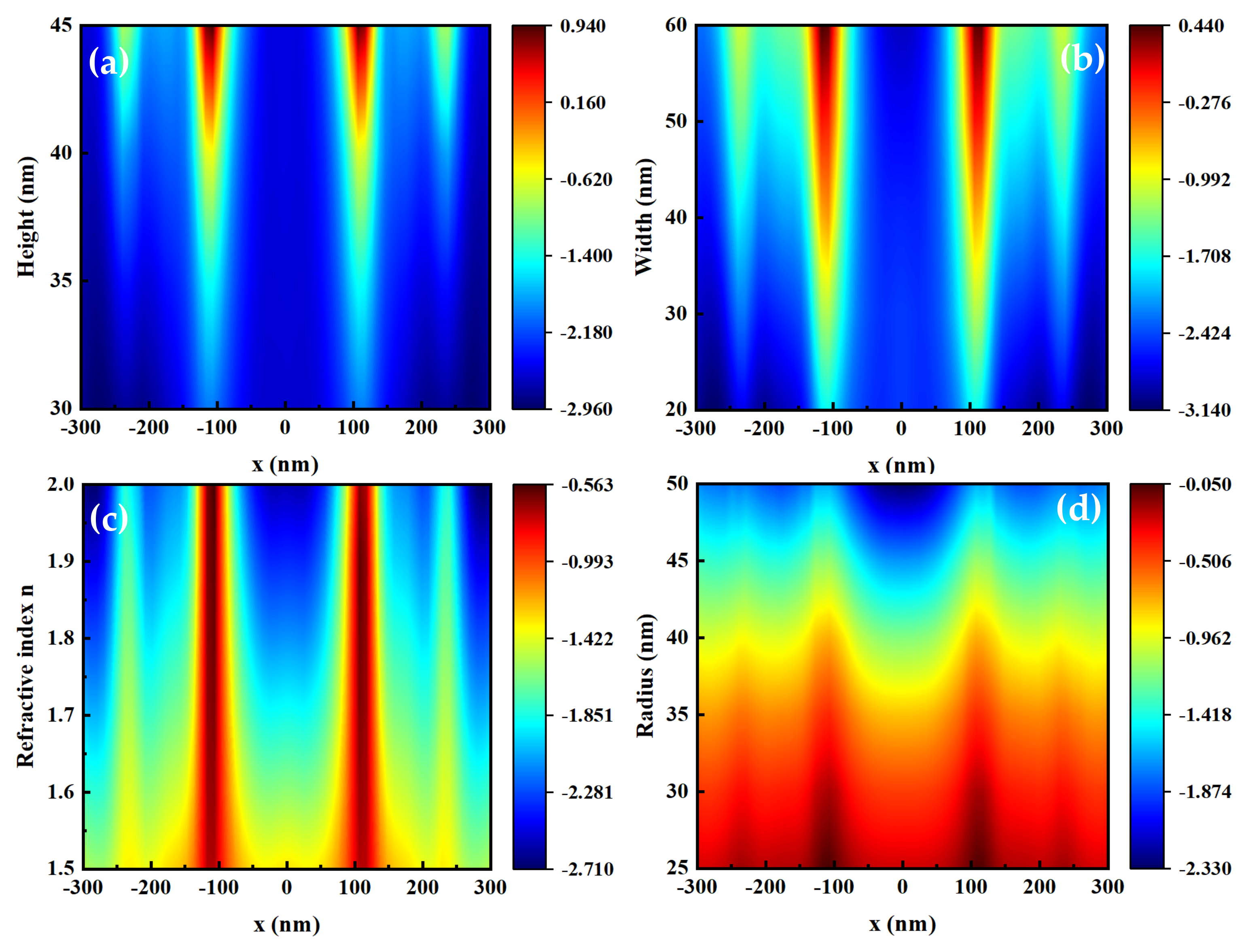
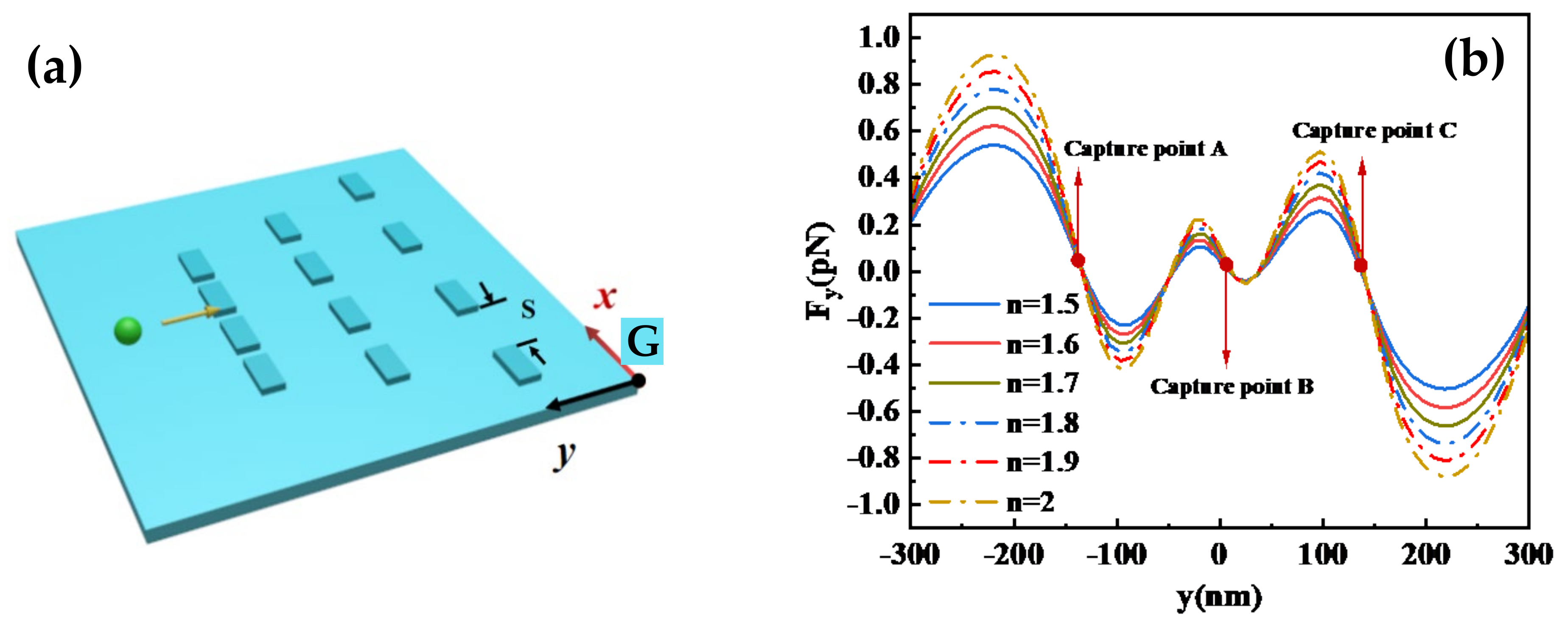
3. Results and Discussion
4. Conclusions
Author Contributions
Funding
Institutional Review Board Statement
Informed Consent Statement
Data Availability Statement
Conflicts of Interest
References
- Ashkin, A. Acceleration and trapping of particles by radiation pressure. Phys. Rev. Lett. 1970, 24, 156–159. [Google Scholar] [CrossRef] [Green Version]
- Perkins, T.T.; Quake, S.R.; Smith, D.; Chu, S. Surface vibrational spectroscopic studies of hydrogen bonding and hydrophobicity. Science 1994, 264, 826–828. [Google Scholar]
- Pralle, A.; Florin, E.; Stelzer, E.H.K.; Horber, J.K.H. Local viscosity probed by photonic force microscopy. Appl. Phys. A 1998, 66, S71–S73. [Google Scholar] [CrossRef]
- Greenleaf, W.J.; Woodside, M.T.; Abbondanzieri, E.A.; Block, S.M. Passive all-optical force clamp for high-resolution laser trapping. Phys. Rev. Lett. 2005, 95, 208102. [Google Scholar] [CrossRef] [Green Version]
- Grier, D.G. A revolution in optical manipulation. Nature 2003, 424, 810–816. [Google Scholar] [CrossRef]
- Li, H.; Ren, Y.; Li, Y.; He, M.; Gao, B.; Qi, H. Nanoparticle manipulation using plasmonic optical tweezers based on particle sizes and refractive indices. Opt. Express 2022, 30, 34092. [Google Scholar] [CrossRef]
- SamadiSamadi, M.; Alibeigloo, P.; Aqhili, A.; Khosravi, M.A.; Saeidi, F.; Vasini, S.; Ghorbanzadeh, M.; Darbar, S.; Moravvej-Farshi, M.K. Plasmonic tweezers: Towards nanoscale manipulation. Opt. Lasers Eng. 2022, 154, 107001. [Google Scholar] [CrossRef]
- Schuller, J.A.; Barnard, E.S.; Cai, W.; Jun, Y.C.; White, J.S.; Brongersma, M.L. Plasmonics for extreme light concentration and manipulation. Nat. Mater. 2010, 9, 193–204. [Google Scholar] [CrossRef] [PubMed]
- Barnes, W.L.; Dereux, A.T.; Ebbesen, W. Surface plasmon subwavelength optics. Nature 2003, 424, 824–830. [Google Scholar] [CrossRef] [PubMed]
- Yoo, D.; Gurunatha, K.L.; Choi, H.-K.; Mohr, D.A.; Ertsgaard, C.T.; Gordon, R.; Oh, S.-H. Low-Power Optical Trapping of Nanoparticles and Proteins with Resonant Coaxial Nanoaperture Using 10 nm Gap. Nano Lett. 2018, 18, 3637–3642. [Google Scholar] [CrossRef] [PubMed]
- Satter, S.S.; Mahdy, M.R.C.; Ohi, M.A.R.; Islam, F.; Rivy, H.M. Plasmonic cube tetramers over substrates: Reversal of binding force as the effect of fano resonance and light polarization. J. Phys. Chem. C 2018, 122, 20923–20934. [Google Scholar] [CrossRef]
- Zhang, Q.; Xiao, J.J. Multiple reversals of optical binding force in plasmonic disk-ring nanostructures with dipole-multipole Fano resonances. Opt. Lett. 2013, 38, 4240–4243. [Google Scholar] [CrossRef] [Green Version]
- Pang, Y.; Gordon, R. Optical trapping of a single protein. Nano Lett. 2011, 12, 402. [Google Scholar] [CrossRef] [PubMed]
- Gao, D.; Shi, R.; Huang, Y.; Gao, L. Fano-enhanced pulling and pushing optical force on active plasmonic nanoparticles. Phys. Rev. A 2017, 96, 043826. [Google Scholar] [CrossRef] [Green Version]
- Jiang, M.; Wang, G.; Xu, W.; Ji, W.; Zou, N.; Ho, H.-P.; Zhang, X. Two-dimensional arbitrary nano-manipulation on a plasmonic metasurface. Opt. Lett. 2018, 43, 1602–1605. [Google Scholar] [CrossRef]
- Khurgin, J.B.; Jacob, B. How to deal with the loss in plasmonics and metamaterials. Nat. Nanotechnol. 2015, 10, 2–6. [Google Scholar] [CrossRef] [PubMed]
- Xu, Z.; Song, W.; Crozier, K.B. Optical Trapping of Nanoparticles Using All-Silicon Nanoantennas. ACS Photon. 2018, 5, 4993–5001. [Google Scholar] [CrossRef]
- Yang, Y.; Ren, Y.X.; Chen, M.; Arita, Y.; Rosales-Guzmán, C. Optical trapping with structured light: A review. Adv. Photonics 2021, 3, 034001. [Google Scholar] [CrossRef]
- Xu, Z.; Crozier, K.B. All-dielectric nanotweezers for trapping and observation of a single quantum dot. Opt. Express 2019, 27, 4034. [Google Scholar] [CrossRef] [PubMed]
- Shi, Y.; Song, Q.; Toftul, I.; Zhu, T.; Yu, Y.; Zhu, W.; Tsai, D.P.; Kivshar, Y.; Liu, A.Q. Optical manipulation with metamaterial structures. Appl. Phys. Rev. 2022, 9, 031303. [Google Scholar] [CrossRef]
- Liu, L.; Ge, L. Toroidal dipole resonances by a sub-wavelength all-dielectric torus. Opt. Express 2022, 30, 7491–7500. [Google Scholar] [CrossRef] [PubMed]
- Savinov, V.; Fedotov, V.A.; Zheludev, N.I. Toroidal dipolar excitation and macroscopic electromagnetic properties of metamaterials. Phys. Rev. B 2014, 89, 205112. [Google Scholar] [CrossRef]
- Zhang, X.; Zhang, Q.; Yuan, Y.; Liu, J.; Liu, X. Ultra-directional forward scattering by a high refractive index dielectric T-shaped nanoantenna in the visible. Phys. Letter. A 2020, 384, 126696. [Google Scholar] [CrossRef]
- Xu, C.; Cheng, K.; Li, Q.; Shang, X.; Wu, C.; Wei, Z.; Zhang, X.; Li, H. The dual-frequency zero-backward scattering realized in a hybrid metallo-dielectric nanoantenna. AIP Adv. 2019, 9, 075121. [Google Scholar] [CrossRef] [Green Version]
- Rohrbach, A.; Stelzer, E.H. Optical Trapping of Dielectric Particles in Arbitrary Fields. J. Opt. Soc. Am. A 2001, 18, 839–853. [Google Scholar] [CrossRef]
- Yang, X.; Liu, Y.; Oulton, R.F.; Yin, X.; Zhang, X. Optical Forces in Hybrid Plasmonic Waveguides. Nano Lett. 2011, 11, 321–328. [Google Scholar] [CrossRef]
- Wan, T.; Tang, B. Efficient Prediction and Analysis of Optical Trapping at Nanoscale via Finite Element Tearing and Interconnecting Method. Nanoscale Res. Lett. 2019, 14, 294. [Google Scholar] [CrossRef] [Green Version]
- Ghorbanzadeh, M.; Darbari, S.; Moravvej-Farshi, M.K. Graphene-Based Plasmonic Force Switch. Appl. Phys. Lett. 2016, 108, 111105. [Google Scholar] [CrossRef]
- Novotny, L.; Bian, R.X.; Xie, X.S. Theory of Nanometric Optical Tweezers. Phys. Rev. Lett. 1997, 79, 645. [Google Scholar] [CrossRef] [Green Version]
- Ashkin, A.; Dziedzic, J.M.; Bjorkholm, J.E.; Chu, S. Observation of a Single-Beam Gradient Force Optical Trap for Dielectric Particles. Opt. Lett. 1986, 11, 288–290. [Google Scholar] [CrossRef] [PubMed] [Green Version]
- Xiong, Y.; Liu, X.; Zhang, J.; Wang, X.; Wang, X.; Gao, J.; Yang, H. High-Performance Ultra-Broadband for Polarized Long-Wavelength Infared Light Trapping. Coatings 2022, 12, 1194. [Google Scholar] [CrossRef]
- Palik, E.D. Handbook of Optical Constants of Solids; Academic Press: New York, NY, USA, 1985. [Google Scholar]
- Zhu, J.; Hu, D.; Wang, Y.; Tao, C.; Jia, H.; Zhao, W. Efficient Light Trapping from Nanorod-Like Single-Textured Al-Doped ZnO Transparent Conducting Films. Coatings 2021, 11, 513. [Google Scholar] [CrossRef]
- Wang, S.; Liu, H.; Ma, K.; Ou, Q.; Geng, H.; Lv, F. Effect of Particle Trap on Motion Characteristics of Metal Particles in AC GILs and Parameter Optimization. Coatings 2022, 12, 981. [Google Scholar] [CrossRef]
- Guo, Y.; Liao, Y.; Yu, Y.; Shi, Y.; Xiong, S. Nanoparticle trapping and manipulation using a silicon nanotrimer with polarized light. Opt. Lett. 2020, 45, 5604–5607. [Google Scholar] [CrossRef] [PubMed]
- Li, R.; Zhao, Y.; Ge, Y.; Xu, Z. Optical trapping and manipulation of nanowires using multi-hotspot dielectric nanononamers. AIP Adv. 2022, 12, 065128. [Google Scholar] [CrossRef]
- Li, R.; Zhao, Y.; Li, R.; Liu, H.; Ge, Y.; Xu, Z. Plasmonic optical trapping of nanoparticles using T-shaped copper nanoantennas. Opt. Express 2021, 29, 9826–9835. [Google Scholar] [CrossRef]
- Lin, Y.; Lee, P. Efficient Optical Trapping and Detection of Nanoparticle Via Plasmonic Bowtie Notch. IEEE Photonics J. 2019, 11, 4800610. [Google Scholar] [CrossRef]
- Zhang, W.; Zhang, Y.; Zhang, S.; Wang, Y.; Yang, W.; Min, C.; Yuan, X. Nonlinear modulation on optical trapping in a plasmonic bowtie structure. Opt. Express 2021, 29, 11664–11673. [Google Scholar] [CrossRef]


| References | Characteristics | Wavelength Range (nm) | Optical Force | Structure Diagram |
|---|---|---|---|---|
| [35] | Si nanotrimer on a Si substrate Particle r = 10–15 nm | 600–1200 | One capture point | 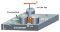 |
| [36] | Si nanononamer on a glass substrate Nanowire r = 15 nm | 1064 | Trapping of multiple nanowires |  |
| [37] | Coupled T-shaped Cu nanoantenna on a glass substrate Particle r = 15 nm | 1064 | One capture point | 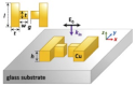 |
| [38] | Au bowtie aperture and Au thin film on a glass substrate Particle r = 50 nm | 1100–1200 | One capture point |  |
| [7] | Coaxial plasmonic aperture (a dielectric ring embedded in a noble metal) Particle r = 5 nm | 400–800 | Two capture point | 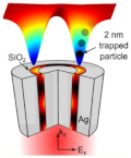 |
| [39] | Gold bowtie structure and ITO film on a glass substrate Particle r = 2 nm | 532 | Two capture point | 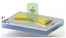 |
| This work | Si-nanostructured array coating on silicon film (SAS film) Particle r = 25–45 nm | 900–1800 | Four capture point | 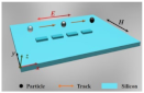 |
Disclaimer/Publisher’s Note: The statements, opinions and data contained in all publications are solely those of the individual author(s) and contributor(s) and not of MDPI and/or the editor(s). MDPI and/or the editor(s) disclaim responsibility for any injury to people or property resulting from any ideas, methods, instructions or products referred to in the content. |
© 2023 by the authors. Licensee MDPI, Basel, Switzerland. This article is an open access article distributed under the terms and conditions of the Creative Commons Attribution (CC BY) license (https://creativecommons.org/licenses/by/4.0/).
Share and Cite
Zhou, W.; Wang, D.; Ren, Y.; Lv, J.; Yu, Y.; Li, W.; Xu, X.; Chu, P.K.; Liu, C. Optical Trapping and Manipulation of Nanoparticles on Plasmonic Silicon-Nanostructured Array Coating on Silicon Film. Coatings 2023, 13, 1388. https://doi.org/10.3390/coatings13081388
Zhou W, Wang D, Ren Y, Lv J, Yu Y, Li W, Xu X, Chu PK, Liu C. Optical Trapping and Manipulation of Nanoparticles on Plasmonic Silicon-Nanostructured Array Coating on Silicon Film. Coatings. 2023; 13(8):1388. https://doi.org/10.3390/coatings13081388
Chicago/Turabian StyleZhou, Wei, Debao Wang, Yanru Ren, Jingwei Lv, Ying Yu, Wei Li, Xinchen Xu, Paul K. Chu, and Chao Liu. 2023. "Optical Trapping and Manipulation of Nanoparticles on Plasmonic Silicon-Nanostructured Array Coating on Silicon Film" Coatings 13, no. 8: 1388. https://doi.org/10.3390/coatings13081388
APA StyleZhou, W., Wang, D., Ren, Y., Lv, J., Yu, Y., Li, W., Xu, X., Chu, P. K., & Liu, C. (2023). Optical Trapping and Manipulation of Nanoparticles on Plasmonic Silicon-Nanostructured Array Coating on Silicon Film. Coatings, 13(8), 1388. https://doi.org/10.3390/coatings13081388