Article

Optimization of Large-Area PM6:D18-CL:Y6 Ternary Organic Solar Cells: The Influence of Film Thickness, Annealing Temperature, and Connection Configuration

1
College of Electron and Information, University of Electronic Science and Technology of China Zhongshan Institute, Zhongshan 528402, China
2
School of Optoelectronic Science and Engineering, University of Electronic Science and Technology of China, Chengdu 610054, China
*
Author to whom correspondence should be addressed.
Coatings 2023, 13(9), 1561; https://doi.org/10.3390/coatings13091561
Submission received: 5 August 2023 / Revised: 24 August 2023 / Accepted: 4 September 2023 / Published: 6 September 2023

Abstract

:
This research focuses on the fabrication and optimization of large-area PM6:D18-CL:Y6 ternary organic solar cells, with a particular emphasis on film thickness, annealing temperature, and the connection configuration’s impact on device performance. The experimental findings indicate that an optimal film thickness of approximately 105 nm fosters the formation of a well-interconnected network, reducing defects and significantly improving both the fill factor, which reaches 46.2%, and the power conversion efficiency (PCE) at 7.2%. An annealing temperature of 110 °C stands out as the ideal condition, resulting in the highest PCE of 8.15%. Notably, excessively high annealing temperatures lead to material aggregation, compromising device performance. Regarding the connection configurations, the study demonstrates that the 5-series 4-parallel arrangement surpasses traditional setups, achieving an impressive output power of 0.11 W. In conclusion, the meticulous control of the film thickness and annealing temperature is paramount for achieving a high PCE in large-area PM6:D18-CL:Y6 ternary organic solar cells. The 5-series 4-parallel configuration exhibits considerable promise for an enhanced power output, offering valuable insights into the development and industrialization of large-area organic solar cells.

1. Introduction

To date, the high-performance area of organic solar cell devices is typically around 0.1 cm2 [1,2,3], which is not suitable for their connection to form photovoltaic cell modules. To facilitate the industrialization of organic solar cells and establish large-area devices as fundamental units of battery components, addressing this challenge is imperative. At present, two primary developmental trajectories are under exploration: the direct fabrication of large-area devices and the production of large-area devices through series and parallel interconnections. Hong et al. [4] proposed an innovative serial module design that allows for device serial connections without patterning the charge transport layer. They successfully prepared a 4.15 cm2 device using the method of slot-die coating, achieving a photovoltaic conversion efficiency of 7.5%. Wang et al. [5] used blade coating to deposit a ternary blend of PBDB-T:ITIC: PC71BM on a customized metal mask electrode, resulting in a 216 cm2 serial device with a photovoltaic conversion efficiency of 7.7%. Jeong et al. [6] demonstrated an efficient low-temperature printing method for large-area non-fullerene-based organic solar cell modules. By studying the relationship between the concentration of the PTB7-Th:EH-IDTBR blend solution and the film performance, they prepared an 85 cm2 large-area module with an outstanding performance, achieving a peak efficiency of 8.18% and a geometric fill factor of 85%. Zhang et al. [7] achieved the precise control of the crystallinity between PBDB-T:ITIC and introduced FOIC to form a highly balanced crystallinity in the thin film, thus improving the charge carrier mobility and significantly enhancing the fill factor. As a result, they achieved a high power conversion efficiency (PCE) value of 9.81% on a 1.05 cm2 device area. Pan et al. [8] designed and prepared a double-layer electron transport layer to reduce the defects in the electron transport layer and silver nanowire electrode, thereby enhancing the charge carrier collection. The layer consisted of sol-gel ZnO and ZnO nanocrystal layers, and they prepared flexible devices with PM6:Y6 as the active layer, achieving efficiencies of 14.29% and 13.08% for 1 and 4 cm2 devices, respectively. Zheng et al. [9] inserted a conjugated polyelectrolyte (PCP Li) between the Ag electrode and PEDOT:PSS layer to improve the connection interface. They fabricated a 1 cm2 device based on the PBDB-T-2F:Y6:PC71BM active layer on a polyimide substrate, achieving a PCE of 15.56% and setting a new record for flexible organic photovoltaic (OPV) devices. With the continuous improvement in organic solar cell efficiency, it is crucial to accelerate its commercialization [10,11,12,13]. Therefore, it is necessary to explore the process of preparing large-area devices and improve the photovoltaic conversion efficiency of large-area organic solar cells through process optimization and battery structure design.
To date, there are several fabrication methods for large-area organic solar cell devices, including spin-coating, inkjet printing, blade coating, and slot-die coating [14,15,16]. Among them, spin-coating stands out due to its high repeatability, film stability, and precise control of film thickness, making it particularly suitable for studying key factors, such as film thickness, roughness, and annealing temperature, which influence the performance of large-area devices [17,18,19,20,21,22]. For small-area devices, increasing the film thickness is beneficial for enhancing light absorption and exciton generation, leading to an improved photovoltaic performance [23,24,25,26]. However, for large-area devices, excessive film thickness may introduce defects and organic material aggregation, resulting in a decrease in the fill factor. Therefore, the optimization of the morphology and film thickness of the active layer is necessary to improve the fill factor [27,28,29,30,31]. Additionally, thin-film annealing is a crucial thermal treatment process that significantly impacts the film quality [32,33,34,35]. The choice of annealing temperature critically influences the surface morphology and vertical phase separation of the active layer. However, the active layer is sensitive to the annealing temperature, and both excessively high and low temperatures may lead to unfavorable outcomes [36,37,38,39,40]. Hence, determining the optimal annealing temperature is of paramount importance for preparing large-area devices.
In this paper, we fabricate large-area ternary organic solar cell devices with an area of 1.72 cm2. The effects of film thickness and annealing temperature on the morphology of the active layer are investigated. The optimal film thickness and annealing temperature are determined at the corresponding optimum spin-coating speed. The prepared large-area devices achieved an efficiency of 8.15%. Additionally, we conduct comprehensive characterization and testing to analyze the underlying mechanisms. Additionally, we utilize Python 3.9.2 for software simulations to investigate various connection methods for assembling solar cell components. By comparing the output power, output current, and output voltage, we identify the most suitable connection approach as a series–parallel hybrid configuration.

2. Materials and Methods

2.1. Experimental Materials

The main materials used in this experiment were PM6,Y6, D18-CL, ethylene glycol methyl ether, ethanolamine, zinc acetate dihydrate, MoO3, Ag, acetone, isopropanol, chloroform, and ITO transparent conductive glass.

2.2. Cleaning of ITO Glass Substrates

The ITO glass substrate was carefully picked up using tweezers and placed into a pre-cleaned beaker. Deionized water was then poured into the beaker, and a small amount of detergent was added. Subsequently, the beaker containing the ITO glass substrate was placed into an ultrasonic cleaning machine for ultrasonic cleaning. The cleaning parameters were set to a cleaning frequency of 90 Hz, a cleaning temperature of 40 °C, and a cleaning time of 20 min. After ultrasonic cleaning, the ITO glass substrate was further cleaned using acetone and isopropanol following the same procedure. Finally, a clean and dry ITO glass substrate was obtained.

2.3. UV-Light Cleaning

Using an ultraviolet ozone cleaning machine, the internal chamber of the machine was first cleaned with a lint-free cloth. The power was then turned on and the machine was preheated for 15 min to ensure that the ultraviolet lamp reached its rated power and operated steadily. The internal chamber of the machine was also cleaned during this preheating process. After the preheating was completed, the ITO glass substrate with the conductive film facing upwards was placed into the cleaning machine for ultraviolet cleaning, which lasted for 20 min.

2.4. Transport Layer Film Preparation

The preparation methods for the electron transport layer mainly included spin-coating and vacuum evaporation. For the ZnO electron transport layer, a spin-coating method was employed to fabricate the thin film. On the other hand, the MoO3 hole transport layer was prepared using a vacuum evaporation method.

2.5. Active Layer Film Preparation

When preparing the active layer thin film using the spin-coating method, it is essential to pay attention to the mixing condition of the active layer solution before spin-coating. The ambient temperature can also affect the solubility of the solution to some extent. It is recommended to use dynamic spin-coating instead of static spin-coating because the latter may result in a non-uniform film thickness. During the spin-coating process, it is necessary to coordinate the spinning speed and time to control the film thickness effectively. After completing the spin-coating, annealing treatment should be initiated promptly.

2.6. Electrode Preparation

Electrodes were prepared by vacuum vapor deposition using Ag as the raw material for the top electrode.

3. Results and Discussion

3.1. Effect of Film Thickness and Annealing Temperature on the Performance of Large-Area Devices

Recent advancements in organic solar cell research have introduced innovative approaches to enhance photovoltaic efficiency. A ternary solar cell structure, inspired by M.C. Quiles et al. [41], has emerged as a solution to broaden the absorption spectrum, while star-shaped 3D twisted acceptors, as explored by Khan et al. [42], have demonstrated remarkable photovoltaic potential. Additionally, studies by Ul Ain et al. [43] on p-conjugated donor compounds and the research led by Khalid et al. [44] in the rational design of non-fullerene chromophores offer insights into improved charge transfer properties and novel materials for energy device fabrication.
Non-fullerene acceptor (NFA) materials have emerged as promising organic materials in the field of organic solar cells, owing to their notable advantages, such as high optical absorption capability and tunable energy levels. In contrast to fullerenes, which present challenges in terms of controllable synthesis and high production costs, NFAs offer the advantage of relatively lower manufacturing costs. Furthermore, considering the process aspect, the ease of material accessibility becomes particularly significant in the context of organic solar cell research. In this work, we fabricated 1.76 cm2 ternary organic solar cells by incorporating the novel non-fullerene acceptor material D18-CL into the PM6:Y6 binary system (Figure 1a). The active layer of the large-area devices was prepared using a PM6:D18-CL:Y6 blend ratio of 0.8:0.2:1.2, with a solute-to-solvent ratio of 14 mg/mL. To investigate the effect of different film thicknesses, we conducted a comparative experiment by varying the spin-coating parameters for the active layer preparation. The spin-coating speeds were set to 2500, 3000, 3500, and 4000 rpm, resulting in corresponding film thicknesses of 135, 120, 105, and 90 nm, respectively. In addition, we conducted a controlled experiment to optimize the active layer morphology by varying the annealing temperatures. The annealing temperatures were set to 90, 100, 110, and 120 °C.

3.1.1. Effect of Film Thickness on the Photovoltaic Performance of Large-Area Devices

To investigate the impact of different active layer film thicknesses on large-area PM6:D18-CL:Y6 ternary organic solar cell devices, we performed J-V testing using an OAI simulator system. Figure 1b shows the J-V curves for four different spin-coating speeds: 2500, 3000, 3500, and 4000 rpm. In Figure 1c,d, we depict the fundamental structure of a solar cell alongside the chemical structures of the three organic compounds. From the curves, it is evident that the overall photovoltaic performance of the large-area devices is significantly lower compared to that of small-area cells. The J-V curves of large-area devices appear smoother, with a reduced slope at the inflection points, indicating a lower fill factor (FF). From Table 1, it can be seen that as the spin-coating speed increases, the film thickness decreases due to the increased centrifugal force causing more active layer solution to be thrown off the substrate.

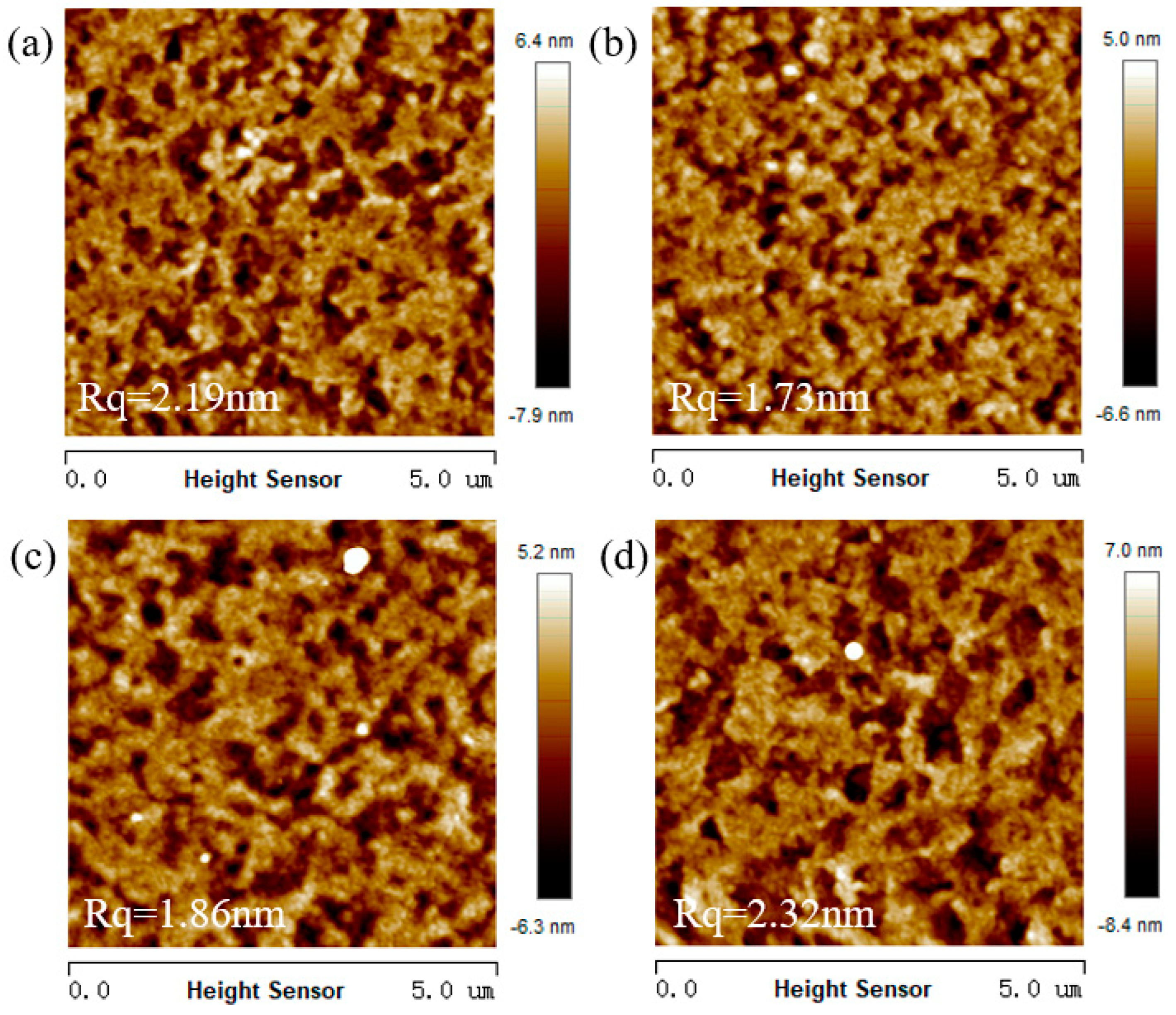
3.1.2. Effect of Film Thickness on the Morphology of the Active Layer in Large-Area Devices

To explore the impact of different active layer film thicknesses on large-area PM6:D18-CL:Y6 ternary organic solar cell devices, we first characterized the presence of large molecular aggregates on the surface of the active layer using metallographic microscopy. Figure 2 shows the magnified and 100× metallographic microscopy images, revealing that with an increase in film thickness (corresponding to a decrease in the spin-coating speed), the phenomenon of large molecular aggregates on the film surface becomes more pronounced. The increase in both the size and quantity of molecular aggregates on the film surface was observed, with the presence of numerous aggregates characterized by larger particle sizes. This phenomenon results in the creation of higher built-in potential barriers, which are detrimental to the dissociation of excitons and adversely affect the transport of charge carriers. Additionally, an elevated non-radiative recombination rate is attributed to the increased distance required for charge carrier transport around the molecular clusters, significantly contributing to the observed low fill factor in the large-area devices.
Furthermore, we also employed Bruker atomic force microscopy (AFM) to observe the precise surface morphology of the films under different film thicknesses, as shown in Figure 3. The 2D AFM images reveal the root mean square roughness (Rq) values, which indicate the surface roughness of the films. When the film thickness increases from 90 to 105 nm, the Rq value decreases from 2.19 to 1.73 nm. This reduction in Rq is primarily attributed to the decrease in defects within the active layer film, leading to a smoother surface and the formation of a well-interconnected network structure. The reduced presence of light-colored regions in the images indicates a decrease in the number of defects. However, as the film thickness is further increased to 120 nm and up to 135 nm, the Rq values increase to 1.86 and 2.32 nm, respectively, representing an almost twofold increase in the surface roughness. The enlargement of dark-colored regions in the images indicates the deterioration in the surface morphology quality. This suggests that the molecular side-chain arrangement becomes more disordered, leading to an increased formation of molecular aggregates, and the increase in Ohmic contacts at the interfaces significantly reduces the exciton dissociation efficiency.
In the AFM 3D image (Figure 4), a more intuitive three-dimensional representation of the film’s defects, molecular aggregation, and vertical phase separation is provided. For the film with a thickness of 90 nm, the vertical height difference is the smallest compared to other film thicknesses, indicating fewer surface protrusions but more surface depressions (dark regions), implying the presence of more defects. In contrast, the film with a thickness of 105 nm exhibits a vertical height difference of 5.8 nm, with fewer surface protrusions and a uniform and smooth surface, indicating the excellent self-assembly of organic materials and the formation of a well-interconnected vertically phase-separated network structure. For the films with thicknesses of 120 and 135 nm, the corresponding vertical height differences increase to 5.8 and 7.7 nm, respectively, almost doubling the height difference compared to the 105 nm film. The surface protrusions become larger and more numerous, and their area sizes also increase, indicating the formation of larger molecular aggregates on the surface. This results in an increased carrier transport distance and reduced carrier transport efficiency, leading to a negative impact on the photovoltaic performance of large-area organic solar cell devices. Consequently, both the short-circuit current and fill factor are reduced to varying degrees, consistent with the decrease in the photovoltaic performance. The AFM 3D results further confirm that the optimal film thickness for the device is 105 nm, which is consistent with the conclusion drawn from the J-V curves earlier. Therefore, the combination of AFM and J-V analyses demonstrates that a film thickness of 105 nm produces to the best performance for the large-area PM6:D18-CL:Y6 ternary organic solar cell device, where defects, molecular aggregation, and vertical phase separation are well-balanced, thereby enhancing the overall photovoltaic efficiency.

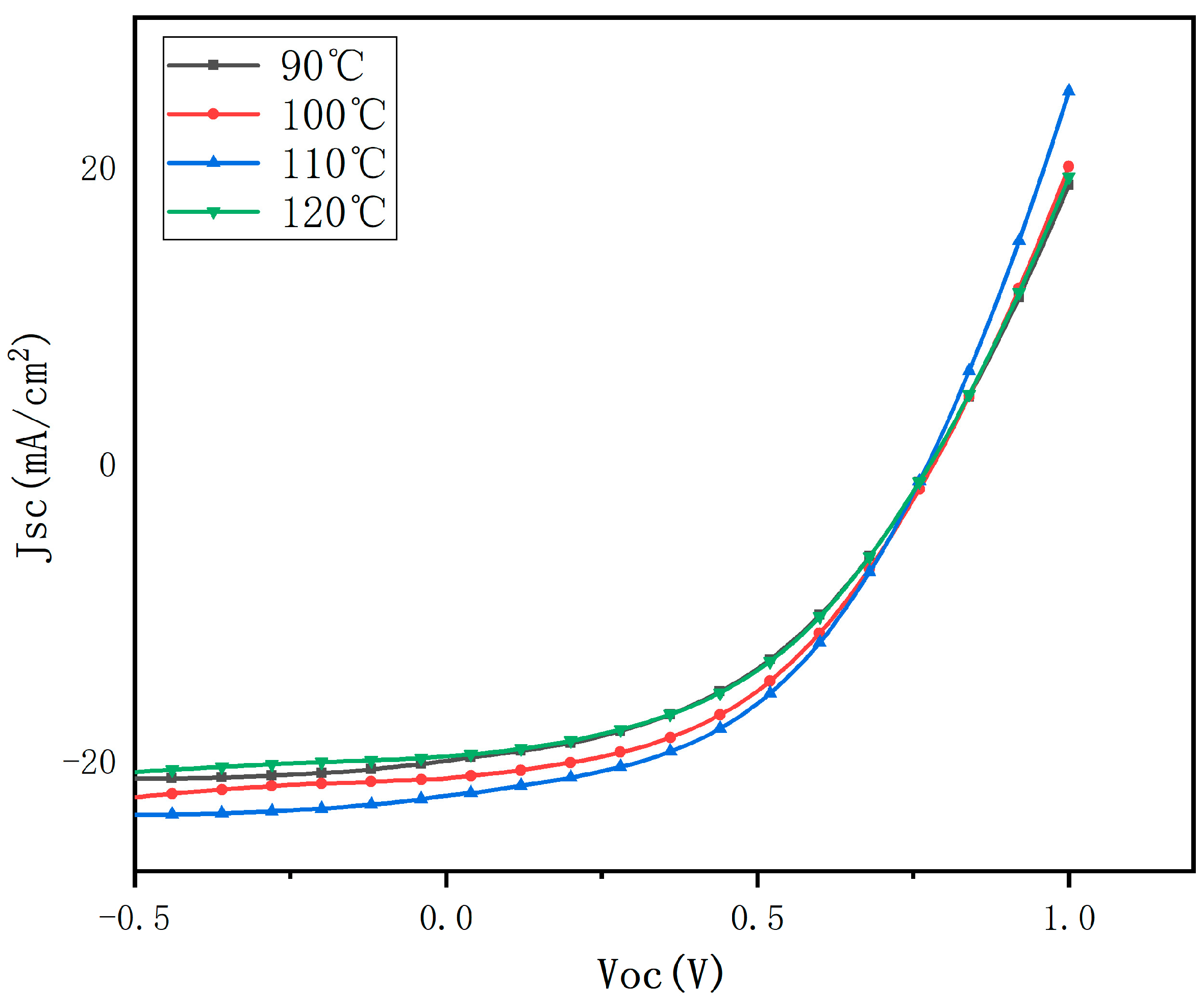
3.1.3. Effect of Annealing Temperature on the Photovoltaic Performance of Large-Area Devices

Annealing treatment has a significant impact on the film formation quality and device performance of organic solar cells. To investigate the effect of different annealing temperatures on large-area organic solar cell devices, four temperature plans (90, 100, 110, and 120 °C) were set to find the most favorable annealing temperature for the devices. The annealing time was kept consistent at 10 min. I-V tests were conducted on the prepared large-area devices, and the corresponding J-V curves are shown in Figure 5. The analysis of the J-V curves reveals that the device annealed at 110 °C exhibited a steeper slope at the J-V curve inflection point and the highest short-circuit current cut-off value, indicating the best performance at this annealing temperature. By combining the data from Table 2 for a specific analysis of other key parameters, it can be observed that the lowest photovoltaic efficiency is 6.98% at an annealing temperature of 90 °C. Increasing the annealing temperature from 90 to 100 °C led to an improvement in the photovoltaic efficiency to 7.68%, with a performance enhancement of 0.7%. Both the fill factor (FF) and short-circuit current also increased. At an annealing temperature of 110 °C, the photovoltaic performance of the device was further enhanced, with a corresponding photovoltaic efficiency of 8.15%, which was the highest efficiency achieved for the prepared large-area devices. The fill factor and short-circuit current were 46.6% and 22.56 mA/cm2, respectively, at this temperature. The significant enhancement in the device performance at 110 °C was attributed to the appropriate temperature improving the self-assembly ability of the organic active layer material, leading to a more ordered arrangement of acceptor molecule side chains. This optimization of the phase separation between D18-CL, PM6, and Y6 facilitated the improved separation efficiency of excitons. Additionally, the film’s ability to absorb photons was enhanced due to the well-separated phase structure, increasing the internal reflection and refraction of incident light within the film. This also explains the increase in the short-circuit current density. However, when the temperature was raised to 120 °C, both the photovoltaic performance and fill factor started to decline, reaching 7% and 45.1%, respectively. The short-circuit current density experienced the greatest decrease of 2.55 mA/cm2. This was mainly attributed to the high temperature inducing molecular aggregation in the organic film, resulting in the deterioration of the surface morphology of the film. The aggregation sites impacted the exciton dissociation, and the increased carrier transport distance led to a decrease in the carrier mobility, ultimately affecting the overall device performance.

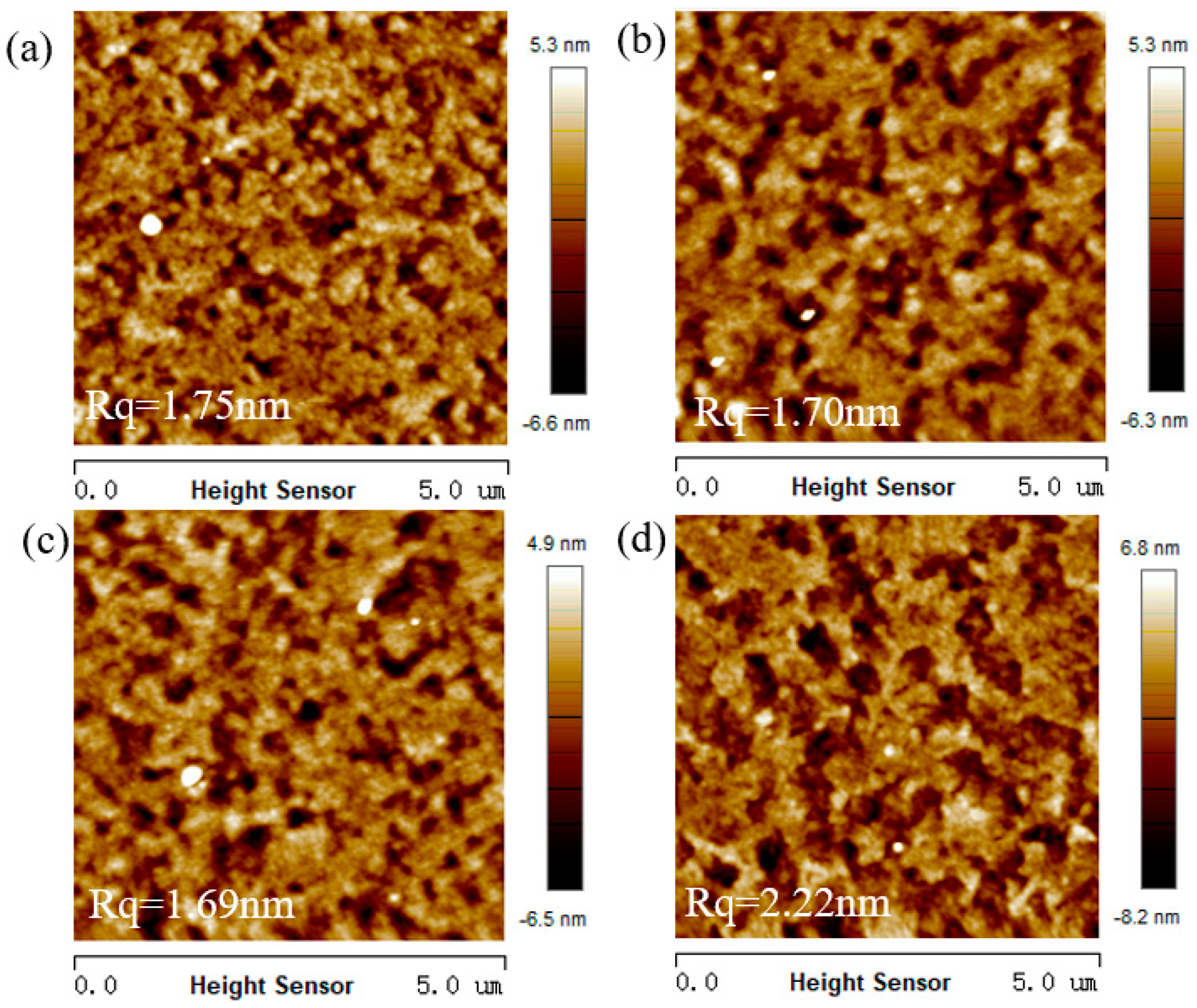
3.1.4. Effect of Annealing Temperature on the Morphology of Active Films

To investigate the influence of different annealing temperatures on the surface morphology of the active layer thin film in large-area PM6:D18-CL:Y6 ternary organic solar cell devices, organic active material clusters on the film surface were characterized using a BX51 metallurgical microscope, as shown in Figure 6. The magnification parameters remained consistent with the previous observations. As the annealing temperature increased, small molecular clusters began to appear on the film surface. Figure 6d corresponds to an annealing temperature of 120 °C, where the number of molecular clusters is the highest, and some clusters are relatively large in size. This indicates that excessively high temperatures can lead to a deterioration in the film formation quality on the surface, subsequently adversely affecting the fill factor of the thin film.
Subsequently, the active layer thin films annealed at different temperatures were further characterized using the Bruker atomic force microscope (AFM), as shown in Figure 7. The two-dimensional AFM images display the root mean square roughness (Rq) values for annealing temperatures ranging from 90 to 120 °C, which were measured to be 1.75, 1.70, 1.69, and 2.22 nm, respectively. The Rq values exhibit a trend of increasing and then decreasing. The minimum Rq value of 1.69 nm corresponds to an annealing temperature of 110 °C, indicating that annealing at 110 °C is the most favorable for achieving a smooth film formation. At this temperature, the molecular arrangement of the organic material in the thin film becomes more ordered, forming a well-separated structure that improves the fill factor and short-circuit current of the device. This finding supports the conclusion that annealing at 110 °C is optimal for enhancing the overall performance of the large-area PM6:D18-CL:Y6 ternary organic solar cell device.
From the three-dimensional AFM height map in Figure 8, it can be observed that the height differences at 90, 100, and 110 °C are not significantly different, measuring 6, 5.8, and 5.7 nm, respectively. However, at 90 °C, the thin film exhibits a higher number of defects, which allows more light to penetrate through the film at the defect locations. This weakens the light absorption capability of the thin film, resulting in a decrease in the short-circuit current and an impact on the fill factor of the device. At 120 °C, the height difference significantly increases compared to other temperatures, with more protrusions and larger areas in the active layer thin film. This indicates the severe aggregation of the active layer molecules on the surface and a deterioration of the phase-separated structure. Consequently, the dissociation efficiency of excitons is negatively affected. Moreover, due to the increased molecular aggregation, the carrier transport distance becomes longer, leading to delayed carrier transfer to the transition layer and resulting in a more non-radiative recombination, which further reduces the short-circuit current density and fill factor of the device.

3.2. Series–Parallel Simulations of Battery Modules Based on Large-Area Devices

At present, organic solar cells are typically limited to small areas in the laboratory and are not directly suitable for practical photovoltaic modules. Regarding the connection configuration of solar cell modules, a series connection increases the output voltage but also increases the total resistance and the risk of single cell failure. A parallel connection increases the output current but is not conducive to power improvement and adds complexity. Therefore, a combination of series and parallel connections has become a solution, facilitating the matrix connection, especially suitable for the all-solution fabrication and roll-to-roll process of organic solar cells. Achieving the connection configuration of large-area solar cell modules is crucial for fully utilizing the photoconversion energy and is an important research direction for industrialization. In this work, we mainly simulated and studied the output voltage, output current, and output power of a solar cell module composed of nine basic cell units under different series–parallel connection configurations. Specifically, we explored eight different configurations: nine cells in series, seven cells in series with two cells in parallel, six cells in series with three cells in parallel, five cells in series with four cells in parallel, four cells in series with five cells in parallel, three cells in series with six cells in parallel, seven cells in series with two cells in parallel, and all nine cells in parallel. We obtained the I-V characteristic curves and P-V characteristic curves for each configuration and analyzed the combined results to gain insights into their performance.

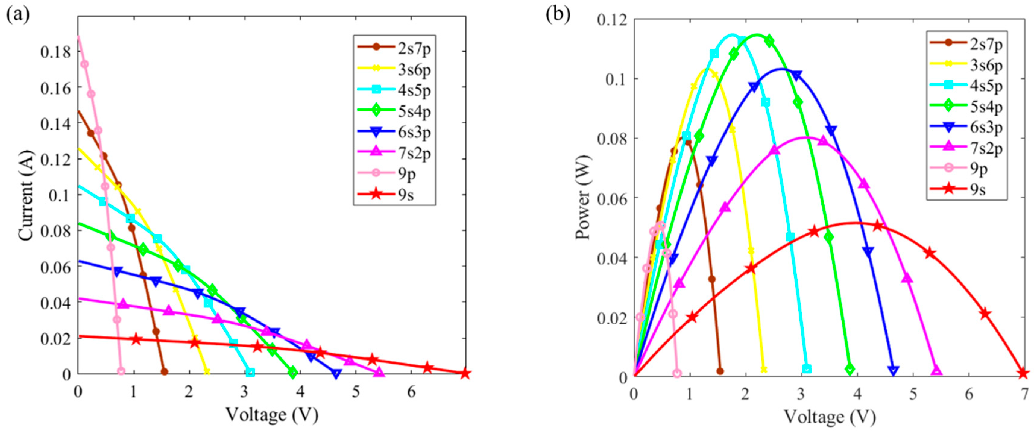
3.2.1. Simulation and Analysis of the Series–Parallel Connections of Battery Components

By using Python (verison 3.9.2) to simulate different connection methods of battery components, we obtained the simulation results in the I-V characteristic curve in Figure 9a. From the curve, it can be observed that: when nine battery cells are connected in series, the open-circuit voltage is the highest among all the connection methods, reaching 7.02 V, while the short-circuit current is the lowest, at 0.021 A. This was because the series connection increased the voltage; however, only one battery cell passed the current, resulting in a lower short-circuit current. With the increase in the number of battery cells connected in parallel, the open-circuit voltage gradually decreased, while the short-circuit current gradually increased. When nine battery cells were connected in parallel, the short-circuit current was the highest among all the connection methods, at 0.189 A, while the open-circuit voltage was the lowest, at 0.78 V. This was due to the parallel connection method increasing the current; however, as the number of parallel battery cells increased, the voltage decreased accordingly.
Through the analysis of the P-V characteristic curve in Figure 9b and in combination with Table 3, it can be observed that when nine battery cells are connected in series and in parallel, the output power P is the same at 0.05 W. This indicates that both series and parallel connections do not provide a power gain for the battery components. As the number of battery cells connected in parallel increased and the number of cells connected in series decreased, the output power of the battery module gradually increased. Among the different connection methods, the highest output power was achieved when using four cells in series and five cells in parallel, as well as five cells in series and four cells in parallel, both reaching 0.11 W. Among these, the connection method with five cells in series and four cells in parallel yielded a higher output voltage of 2.2 V compared to the connection method with four cells in series and five cells in parallel, which corresponded to the open-circuit voltage. As the number of parallel basic units increased further, the output power began to decrease. Overall, under the same illumination intensity and environmental temperature conditions, the connection method with four cells in series and five cells in parallel achieved the highest output power and the highest power point (Pmpp) corresponded to a relatively high voltage. This makes it suitable for powering portable electronic devices, such as electronic watches.

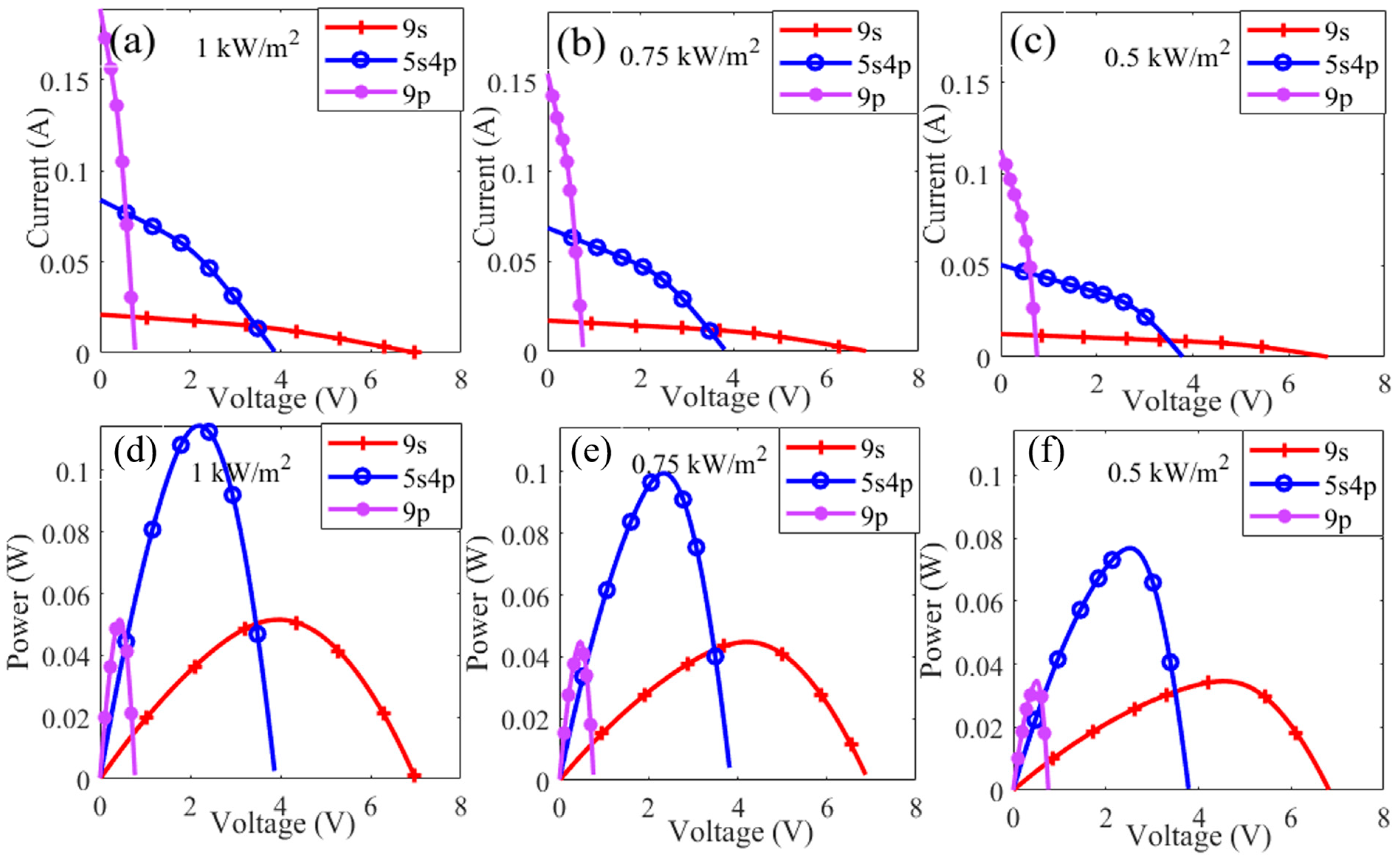
3.2.2. Simulation Analysis of Battery Modules with Different Light Intensities

Based on the previous simulation results, further investigations were conducted to explore the performance variations of three different connections, namely, the serial connection of nine battery cells, parallel connection of nine battery cells, and serial connection of five battery cells with four battery cells in parallel, under different light intensities. Three light intensities were set at 1000, 750, and 500 W/m2, respectively. Figure 10a–c shows the corresponding I-V curves and Figure 10d–f displays the corresponding P-V curves. From Figure 10a–c, it can be observed that as the light intensity decreases, the I-V curves shift leftward and downward, indicating reductions in both the open-circuit voltage and short-circuit current. The decrease in the short-circuit current is more significant compared to the decrease in the open-circuit voltage. Analyzing the P-V curves in Figure 10d–f, it is evident that with the decreasing light intensity, the curves shift downward, indicating reductions in the output power at different voltage levels. Additionally, the maximum power points shift to the right, implying that the corresponding voltages increase as the light intensity decreases. Table 4 summarizes the maximum power points for the three connection methods under different light intensities.
Further comparisons were performed among the three connection methods, namely, serial, parallel, and serial connections of five battery cells with four battery cells in parallel, under the same light intensity. The open-circuit voltage, short-circuit current, and output power were analyzed and compared. By superimposing the I-V and P-V curves of the three connection methods under the same light intensity, as shown in Figure 11, it can be observed that, even under different light intensities, the configuration of five battery cells in series with four battery cells in parallel consistently exhibits a higher maximum output power compared to the serial and parallel connection methods. This finding unequivocally demonstrates the superiority of the connection configuration involving five battery cells in series with four battery cells in parallel in terms of achieving a higher output power, irrespective of the variations in the light intensity.

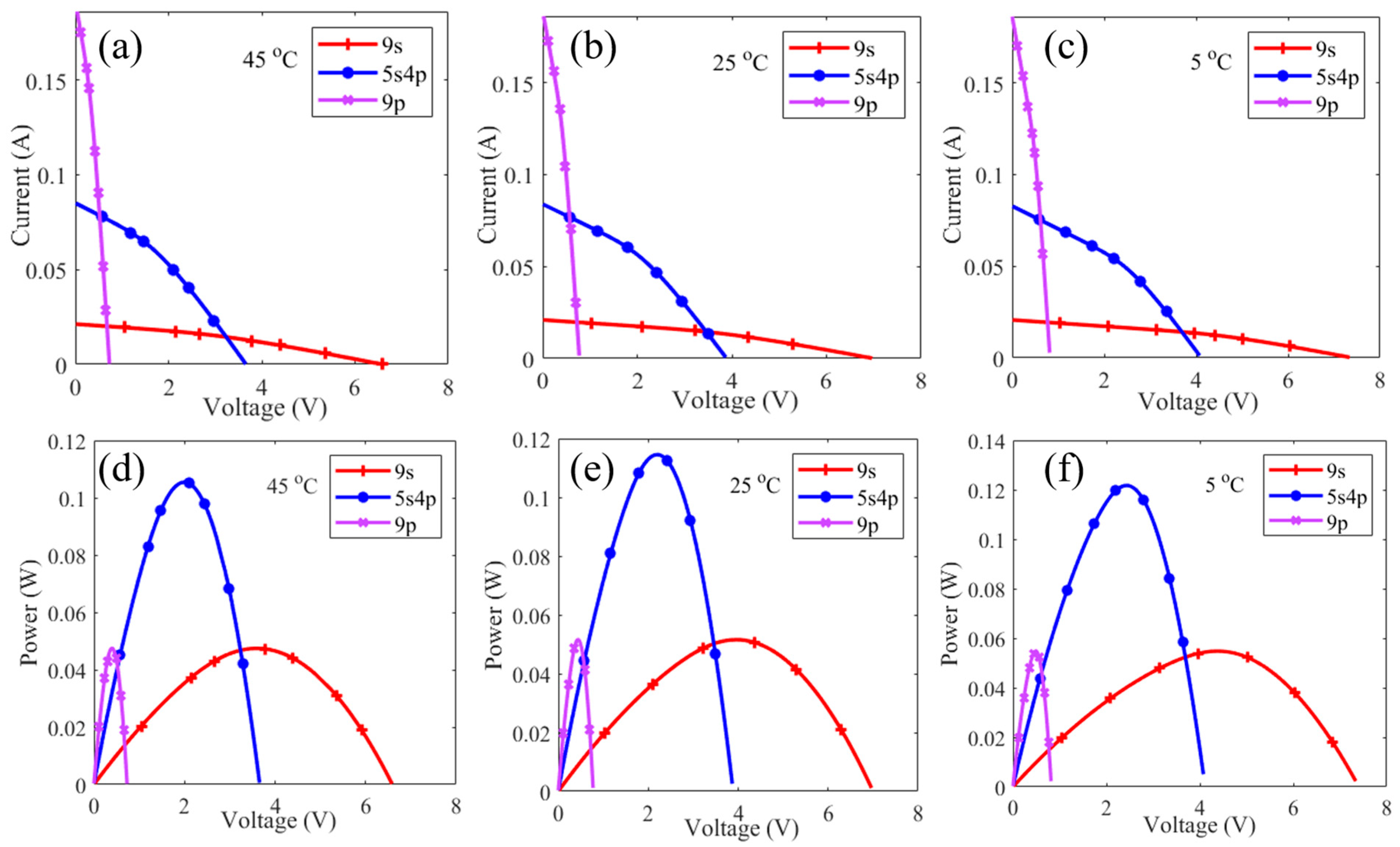
3.2.3. Simulation and Analysis of Battery Components at Different Temperatures

In order to investigate the variations of the open-circuit voltage (Voc), short-circuit current (Isc), and output power under different environmental temperatures, three temperature parameters of 45, 25, and 5 °C were considered. I-V and P-V curves were obtained through simulations, as shown in Figure 12. From the I-V curves, it is evident that as the temperature decreases, the short-circuit current experiences a slight reduction, while the open-circuit voltage exhibits a significant increase. The decrease in temperature enhances the open-circuit voltage with a substantial improvement. The P-V curves demonstrate that lowering the temperature results in an upward shift of the curves, and the maximum power point shifts to higher voltages. This indicates that the reduction in temperature is beneficial for the output power of the battery components, and the corresponding maximum power voltage is increased. At an environmental temperature of 5 °C, the maximum output power and its corresponding voltage are 0.12 W and 2.43 V, respectively. Table 5 summarizes the maximum power points corresponding to different connection configurations at various environmental temperatures. The results illustrate that decreasing the temperature is advantageous for improving the performance of the battery components in terms of the output power, primarily through an increase in the open-circuit voltage and a moderate reduction in the short-circuit current.
Figure 13 illustrates the I-V and P-V curves for three connection configurations, namely, series, parallel, and 5-series 4-parallel, under the three different environmental temperatures. By analyzing the results, it is evident that, across the various temperature conditions, the 5-series 4-parallel connection configuration consistently achieves a higher maximum output power compared to the other two connection configurations. This finding highlights the favorable performance of the 5-series 4-parallel connection approach, as it exhibits a superior capability to harness and optimize the output power of the organic solar cells under different environmental temperature conditions.

4. Conclusions

In summary, this research underscored the paramount significance of fine-tuning film thickness and annealing temperature to attain a greater power conversion efficiency (PCE) in large-area PM6:D18-CL:Y6 ternary organic solar cells. The 5-series 4-parallel connection configuration emerges as the most promising method for achieving an enhanced power output. Furthermore, the study revealed the substantial impact of light intensity and environmental temperature variations on the device performance. These insights hold considerable value for advancing and industrializing large-area organic solar cells.

Author Contributions

Conceptualization, J.Y. and X.W.; methodology, J.Y.; software, X.Y.; validation, J.Y., X.W. and X.Y.; formal analysis, J.L.; investigation, J.L.; resources, Z.Z.; data curation, Z.Z.; writing—original draft preparation, J.Y. and X.W.; writing—review and editing, J.Y. and Z.Z.; visualization, J.Z.; supervision, Z.Z.; project administration, J.Y.; funding acquisition, J.Y. All authors have read and agreed to the published version of the manuscript.

Funding

This research was funded by the National Key R&D Program of China (Grant No. 2018YFB0407100-02).

Institutional Review Board Statement

Not applicable.

Informed Consent Statement

Not applicable.

Data Availability Statement

The raw data can be obtained from the corresponding authors upon reasonable request.

Conflicts of Interest

The authors declare no conflict of interest.

References

  1. Liu, C.H.; Xiao, C.Y.; Xie, C.C.; Li, W.W. Flexible organic solar cells: Materials, large-area fabrication techniques and potential applications. Nano Energy 2021, 89, 106399. [Google Scholar] [CrossRef]
  2. Xiao, Y.F.; Zuo, C.T.; Zhong, J.X.; Wu, W.Q.; Shen, L.; Ding, L.M. Large-Area Blade-Coated Solar Cells: Advances and Perspectives. Adv. Energy Mater. 2021, 11, 2100378. [Google Scholar] [CrossRef]
  3. Xue, P.Y.; Cheng, P.; Han, R.P.S.; Zhan, X.W. Printing fabrication of large-area non-fullerene organic solar cells. Mater. Horiz. 2022, 9, 194–219. [Google Scholar] [CrossRef] [PubMed]
  4. Hong, S.; Kang, H.; Kim, G.; Lee, S.; Kim, S.; Lee, J.H.; Lee, J.; Yi, M.; Kim, J.; Back, H.; et al. A series connection architecture for large-area organic photovoltaic modules with a 7.5% module efficiency. Nat. Commun. 2016, 7, 10279. [Google Scholar] [CrossRef] [PubMed]
  5. Wang, G.D.; Adil, M.A.; Zhang, J.Q.; Wei, Z.X. Large-Area Organic Solar Cells: Material Requirements, Modular Designs, and Printing Methods. Adv. Mater. 2019, 31, e1805089. [Google Scholar] [CrossRef] [PubMed]
  6. Jeong, S.; Park, B.; Hong, S.; Kim, S.; Kim, J.; Kwon, S.; Lee, J.H.; Lee, M.S.; Park, J.C.; Kang, H.; et al. Large-Area Nonfullerene Organic Solar Cell Modules Fabricated by a Temperature-Independent Printing Method. ACS Appl. Mater. Interfaces 2020, 12, 41877–41885. [Google Scholar] [CrossRef]
  7. Zhang, L.; Yang, F.; Meng, X.C.; Yang, S.Z.; Ke, L.L.; Zhou, C.H.; Yan, H.P.; Hu, X.T.; Zhang, S.H.; Ma, W.; et al. Regulating crystallization to maintain balanced carrier mobility via ternary strategy in blade-coated flexible organic solar cells. Org. Electron. 2021, 89, 106027. [Google Scholar] [CrossRef]
  8. Pan, W.; Han, Y.F.; Wang, Z.G.; Gong, C.; Guo, J.B.; Lin, J.; Luo, Q.; Yang, S.F.; Ma, C.Q. An efficiency of 14.29% and 13.08% for 1 cm2 and 4 cm2 flexible organic solar cells enabled by sol-gel ZnO and ZnO nanoparticle bilayer electron transporting layers. J. Mater. Chem. A 2021, 9, 16889–16897. [Google Scholar] [CrossRef]
  9. Zheng, X.J.; Zuo, L.J.; Zhao, F.; Li, Y.K.; Chen, T.Y.; Shan, S.Q.; Yan, K.R.; Pan, Y.W.; Xu, B.W.; Li, C.Z.; et al. High-Efficiency ITO-Free Organic Photovoltaics with Superior Flexibility and Upscalability. Adv. Mater. 2022, 34, e2200044. [Google Scholar] [CrossRef]
  10. Song, J.L.; Zhu, L.; Li, C.; Xu, J.Q.; Wu, H.B.; Zhang, X.N.; Zhang, Y.; Tang, Z.; Liu, F.; Sun, Y.M. High-efficiency organic solar cells with low voltage loss induced by solvent additive strategy. Matter 2021, 4, 2542–2552. [Google Scholar] [CrossRef]
  11. Wang, G.D.; Zhang, J.Q.; Yang, C.; Wang, Y.H.; Xing, Y.; Adil, M.A.; Yang, Y.; Tian, L.J.; Su, M.; Shang, W.Q.; et al. Synergistic Optimization Enables Large-Area Flexible Organic Solar Cells to Maintain over 98% PCE of the Small-Area Rigid Devices. Adv. Mater. 2020, 32, e2005153. [Google Scholar] [CrossRef]
  12. Zhang, S.C.; Chen, H.B.; Wang, P.R.; Li, S.T.; Li, Z.X.; Huang, Y.Z.; Liu, J.; Yao, Z.Y.; Li, C.X.; Wan, X.J.; et al. A Large Area Organic Solar Module with Non-Halogen Solvent Treatment, High Efficiency, and Decent Stability. Sol. RRL 2023, 7, 2300029. [Google Scholar] [CrossRef]
  13. Zheng, Z.; Wang, J.Q.; Bi, P.Q.; Ren, J.Z.; Wang, Y.F.; Yang, Y.; Liu, X.Y.; Zhang, S.Q.; Hou, J.H. Tandem Organic Solar Cell with 20.2% Efficiency. Joule 2022, 6, 171–184. [Google Scholar] [CrossRef]
  14. Andersen, T.R.; Dam, H.F.; Hosel, M.; Helgesen, M.; Carle, J.E.; Larsen-Olsen, T.T.; Gevorgyan, S.A.; Andreasen, J.W.; Adams, J.; Li, N.; et al. Scalable, ambient atmosphere roll-to-roll manufacture of encapsulated large area, flexible organic tandem solar cell modules. Energy Environ. Sci. 2014, 7, 2925–2933. [Google Scholar] [CrossRef]
  15. Haldar, A.; Liao, K.S.; Curran, S.A. Effect of printing parameters and annealing on organic photovoltaics performance. J. Mater. Res. 2012, 27, 2079–2087. [Google Scholar] [CrossRef]
  16. Kubis, P.; Lucera, L.; Machui, F.; Spyropoulos, G.; Cordero, J.; Frey, A.; Kaschta, J.; Voigt, M.M.; Matt, G.J.; Zeira, E.; et al. High precision processing of flexible P3HT/PCBM modules with geometric fill factor over 95%. Org. Electron. 2014, 15, 2256–2263. [Google Scholar] [CrossRef]
  17. Agrawal, N.; Ansari, M.Z.; Majumdar, A.; Gahlet, R.; Khare, N. Efficient up-scaling of organic solar cells. Sol. Energy Mater. Sol. Cells 2016, 157, 960–965. [Google Scholar] [CrossRef]
  18. Chan, M.Y.; Lai, S.L.; Fung, M.K.; Lee, C.S.; Lee, S.T. Doping-induced efficiency enhancement in organic photovoltaic devices. Appl. Phys. Lett. 2007, 91, 089902, Erratum in Appl. Phys. Lett. 2007, 90, 023504. [Google Scholar] [CrossRef]
  19. Choi, S.; Potscavage, W.J.; Kippelen, B. Area-scaling of organic solar cells. J. Appl. Phys. 2009, 106, 054507. [Google Scholar] [CrossRef]
  20. Jin, W.Y.; Ginting, R.T.; Ko, K.J.; Kang, J.W. Ultra-Smooth, Fully Solution-Processed Large-Area Transparent Conducting Electrodes for Organic Devices. Sci. Rep. 2016, 6, 36475. [Google Scholar] [CrossRef]
  21. Kopola, P.; Aernouts, T.; Sliz, R.; Guillerez, S.; Ylikunnari, M.; Cheyns, D.; Valimaki, M.; Tuomikoski, M.; Hast, J.; Jabbour, G.; et al. Gravure printed flexible organic photovoltaic modules. Sol. Energy Mater. Sol. Cells 2011, 95, 1344–1347. [Google Scholar] [CrossRef]
  22. Yu, J.S.; Jung, G.H.; Jo, J.; Kim, J.S.; Kim, J.W.; Kwak, S.W.; Lee, J.L.; Kim, I.; Kim, D. Transparent conductive film with printable embedded patterns for organic solar cells. Sol. Energy Mater. Sol. Cells 2013, 109, 142–147. [Google Scholar] [CrossRef]
  23. Li, H.J.; Liu, S.Q.; Wu, X.T.; Qi, Q.C.; Zhang, H.Y.; Meng, X.C.; Hu, X.T.; Ye, L.; Chen, Y.W. A general enlarging shear impulse approach to green printing large-area and efficient organic photovoltaics. Energy Environ. Sci. 2022, 15, 2130–2138. [Google Scholar] [CrossRef]
  24. Ramos-Hernandez, R.; Calvo, F.D.; Perez-Gutierrez, E.; Percino, M.J. Large area small-molecule thin films deposited by the doctor blade technique implemented with computer numerical control machine. Thin Solid Films 2023, 771, 139787. [Google Scholar] [CrossRef]
  25. Xie, K.C. Reviews of clean coal conversion technology in China: Situations & challenges. Chin. J. Chem. Eng. 2021, 35, 62–69. [Google Scholar] [CrossRef]
  26. Zhang, X.; Zhang, H.; Li, S.L.; Xiao, L.E.; Zhang, S.W.; Han, B.; Kang, J.J.; Zhou, H.Q. Development and application of blade-coating technique in organic solar cells. Nano Res. 2023, 1–18. [Google Scholar] [CrossRef]
  27. Dam, H.F.; Krebs, F.C. Simple roll coater with variable coating and temperature control for printed polymer solar cells. Sol. Energy Mater. Sol. Cells 2012, 97, 191–196. [Google Scholar] [CrossRef]
  28. Dehaj, M.S.; Ahmadi, M.; Ghazanfarpour, S. Inverted bulk heterojunction organic solar cells using optimization of active layer deposition via controlling of doctor blade parameters. Surf. Interfaces 2020, 21, 100694. [Google Scholar] [CrossRef]
  29. Fan, J.Y.; Liu, Z.X.; Rao, J.; Yan, K.R.; Chen, Z.; Ran, Y.X.; Yan, B.Y.; Yao, J.Z.; Lu, G.H.; Zhu, H.M.; et al. High-Performance Organic Solar Modules via Bilayer-Merged-Annealing Assisted Blade Coating. Adv. Mater. 2022, 34, e2110569. [Google Scholar] [CrossRef]
  30. Fukuda, K.; Yu, K.; Someya, T. The Future of Flexible Organic Solar Cells. Adv. Energy Mater. 2020, 10, 2000765. [Google Scholar] [CrossRef]
  31. Hu, X.T.; Liu, S.Q.; Song, Y.L.; Chen, Y.W. New Thin-film Solar Cells: Flexible Design and Printing Manufacturing. Acta Polym. Sin. 2023, 54, 910–926. [Google Scholar]
  32. Ajayan, J.; Nirmal, D.; Mohankumar, P.; Saravanan, M.; Jagadesh, M.; Arivazhagan, L. A review of photovoltaic performance of organic/inorganic solar cells for future renewable and sustainable energy technologies. Superlattices Microstruct. 2020, 143, 106549. [Google Scholar] [CrossRef]
  33. Bai, Y.M.; Zhao, C.Y.; Zhang, S.; Zhang, S.Q.; Yu, R.N.; Hou, J.H.; Tan, Z.A.; Li, Y.F. Printable SnO2 cathode interlayer with up to 500 nm thickness-tolerance for high-performance and large-area organic solar cells. Sci. China-Chem. 2020, 63, 957–965. [Google Scholar] [CrossRef]
  34. Bernardo, G.; Lopes, T.; Lidzey, D.G.; Mendes, A. Progress in Upscaling Organic Photovoltaic Devices. Adv. Energy Mater. 2021, 11, 29. [Google Scholar] [CrossRef]
  35. Chen, D.; Liu, S.Q.; Huang, B.; Oh, J.; Wu, F.Y.; Liu, J.B.; Yang, C.; Chen, L.; Chen, Y.W. Rational Regulation of the Molecular Aggregation Enables A Facile Blade-Coating Process of Large-area All-Polymer Solar Cells with Record Efficiency. Small 2022, 18, e2200734. [Google Scholar] [CrossRef] [PubMed]
  36. Li, Y.; Huang, W.; Zhao, D.J.; Wang, L.; Jiao, Z.Q.; Huang, Q.Y.; Wang, P.; Sun, M.N.; Yuan, G.C. Recent Progress in Organic Solar Cells: A Review on Materials from Acceptor to Donor. Molecules 2022, 27, 1800. [Google Scholar] [CrossRef]
  37. Liao, Y.J.; Hsieh, Y.C.; Chen, J.T.; Yang, L.S.; Jian, X.Z.; Lin, S.H.; Lin, Y.R.; Chen, L.M.; Li, F.H.; Hsiao, Y.T.; et al. Large-Area Nonfullerene Organic Photovoltaic Modules with a High Certified Power Conversion Efficiency. ACS Appl. Mater. Interfaces 2023, 15, 7911–7918. [Google Scholar] [CrossRef]
  38. McDowell, C.; Abdelsamie, M.; Toney, M.F.; Bazan, G.C. Solvent Additives: Key Morphology-Directing Agents for Solution-Processed Organic Solar Cells. Adv. Mater. 2018, 30, e1707114. [Google Scholar] [CrossRef]
  39. Rehman, Z.U.; Haris, M.; Ryu, S.U.; Jahankhan, M.; Song, C.E.; Lee, H.K.; Lee, S.K.; Shin, W.S.; Park, T.; Lee, J.C. Trifluoromethyl-Substituted Conjugated Random Terpolymers Enable High-Performance Small and Large-Area Organic Solar Cells Using Halogen-Free Solvent. Adv. Sci. 2023, 10, e2302376. [Google Scholar] [CrossRef]
  40. Shen, Y.F.; Zhang, H.; Zhang, J.Q.; Tian, C.Y.; Shi, Y.A.; Qiu, D.D.; Zhang, Z.Q.; Lu, K.; Wei, Z.X. In Situ Absorption Characterization Guided Slot-Die-Coated High-Performance Large-Area Flexible Organic Solar Cells and Modules. Adv. Mater. 2023, 35, e2209030. [Google Scholar] [CrossRef]
  41. Campoy-Quiles, M.; Kanai, Y.; El-Basaty, A.; Sakai, H.; Murata, H. Ternary mixing: A simple method to tailor the morphology of organic solar cells. Org. Electron. 2009, 10, 1120–1132. [Google Scholar] [CrossRef]
  42. Khan, M.U.; Khalid, M.; Arshad, M.N.; Khan, M.N.; Usman, M.; Ali, A.; Saifullah, B. Designing Star-Shaped Subphthalocyanine-Based Acceptor Materials with Promising Photovoltaic Parameters for Non-fullerene Solar Cells. ACS Omega 2020, 5, 23039–23052. [Google Scholar] [CrossRef] [PubMed]
  43. ul Ain, Q.; Shehzad, R.A.; Yaqoob, U.; Sharif, A.; Sajid, Z.; Rafiq, S.; Iqbal, S.; Khalid, M.; Iqbal, J. Designing of benzodithiophene acridine based Donor materials with favorable photovoltaic parameters for efficient organic solar cell. Comput. Theor. Chem. 2021, 1200, 113238. [Google Scholar] [CrossRef]
  44. Khalid, M.; Khan, M.U.; Razia, E.T.; Shafiq, Z.; Alam, M.M.; Imran, M.; Akram, M.S. Exploration of efficient electron acceptors for organic solar cells: Rational design of indacenodithiophene based non-fullerene compounds. Sci. Rep. 2021, 11, 19931. [Google Scholar] [CrossRef] [PubMed]
Figure 1. (a) A 1.76 cm2 device physical drawing. (b) J-V curves for devices with different active layer film thicknesses. (c) The organic solar cell device structure. (d) Chemical structures of PM6, Y6, and D18-CL.
Coatings 13 01561 g001
Figure 2. Metallographic images at different active layer film thicknesses: (a) 90, (b) 105, (c) 120, and (d) 135 nm.
Coatings 13 01561 g002
Figure 3. Two-dimensional AFM images of different active layer film thicknesses: (a) 90, (b) 105, (c) 120, and (d) 135 nm.
Coatings 13 01561 g003
Figure 4. Three-dimensional AFM images of different active layer film thicknesses: (a) 90, (b) 105, (c) 120, and (d) 135 nm. (The unit has been clarified).
Coatings 13 01561 g004
Figure 5. J-V curves corresponding to different annealing temperatures.
Coatings 13 01561 g005
Figure 6. Metallographic micrographs (100×) at different annealing temperatures: (a) 90, (b) 100, (c) 110, and (d) 120 °C.
Coatings 13 01561 g006
Figure 7. Two-dimensional AFM images at different annealing temperatures: (a) 90, (b) 100, (c) 110, and (d) 120 °C.
Coatings 13 01561 g007
Figure 8. Three-dimensional AFM images at different annealing temperatures: (a) 90, (b) 100, (c) 110, and (d) 120 °C. (The unit has been clarified).
Coatings 13 01561 g008
Figure 9. (a) Series–parallel I-V curves of battery components. (b) P-V curves of series–parallel connections of battery components.
Coatings 13 01561 g009
Figure 10. I-V/P-V curves of different connections at different light intensities: (a,d) series, (b,e) series–parallel connections, and (c,f) parallel.
Coatings 13 01561 g010
Figure 11. I-V/P-V curves of different connections at the same light intensity: (a,d) 1, (b,e) 0.75, and (c,f) 0.5 kW/m2.
Coatings 13 01561 g011
Figure 12. I-V/P-V curves of three connection types at different temperatures: (a,d) series, (b,e) series–parallel connection, and (c,f) parallel.
Coatings 13 01561 g012
Figure 13. I-V/P-V curves of three connections at the same temperature: (a,d) 45, (b,e) 25, and (c,f) 5 °C.
Coatings 13 01561 g013
Table 1. Performance parameters of devices with different film thicknesses.
Speed (rpm)Thickness (nm)VOC (V)JSC (mA/cm2)FF (%)PCE (%)
4000900.7519.7041.86.2
35001050.7520.5246.27.2
30001200.7719.8945.26.97
25001350.7418.5340.65.54
Table 2. Basic performance parameters of photovoltaic cell devices at different annealing temperatures.
Annealing
Temperature (°C)
VOC (V)JSC (mA/cm2)FF (%)PCE (%)
900.7620.5245.26.98
1000.7821.2646.27.68
1100.7722.5646.68.15
1200.7720.0145.17.00
Table 3. Parameter table of simulation results of series–parallel connections of battery components.
Connection MethodIsc (A)Voc (V)Pmpp (V, W)
9s0.0217.02(3.96, 0.05)
7s2p0.0425.46(3.08, 0.08)
6s3p0.0634.68(2.64, 0.10)
5s4p0.0843.9(2.20, 0.11)
4s5p0.1053.12(1.76, 0.11)
3s6p0.1262.34(1.32, 0.10)
2s7p0.1471.56(0.88, 0.08)
9p0.1890.78(0.78, 0.05)
Table 4. Maximum power points for the three types of connections at different light intensities.
Light Intensity (kW/m2)Series Pmpp (V, W)Series–Parallel Pmpp (V, W)Parallel Pmpp (V, W)
0.5(4.54, 0.03)(2.52, 0.07)(0.50, 0.03)
0.75(4.20, 0.04)(2.33, 0.09)(0.46, 0.04)
1(3.96, 0.05)(2.20, 0.11)(0.44, 0.05)
Table 5. Maximum power points for the three types of connections at different ambient temperatures.
Ambient
Temperature
(°C)
Series Pmpp
(V, W)
Series–Parallel Pmpp
(V, W)
Parallel Pmpp
(V, W)
5(4.37, 0.05)(2.43, 0.12)(0.48, 0.05)
25(3.96, 0.05)(2.20, 0.11)(0.44, 0.05)
45(3.58, 0.04)(1.98, 0.10)(0.40, 0.04)
Disclaimer/Publisher’s Note: The statements, opinions and data contained in all publications are solely those of the individual author(s) and contributor(s) and not of MDPI and/or the editor(s). MDPI and/or the editor(s) disclaim responsibility for any injury to people or property resulting from any ideas, methods, instructions or products referred to in the content.

