Abstract
In order to assess the longevity of foldable electronics, folding or bending tests on model systems need to be performed. However, not all bending tests are created equal in that different configurations lead to different amounts of mechanical damage and thus different electrical responses. Two 90° bending instruments were compared using two model metallic thin film systems on polyimide to establish if the two seemingly similar bending tests yield the same results. The two film systems, namely 300 nm Mo and 130 nm Al on 50 nm Mo, were magnetron-sputtered on polyimide substrates and tested in the custom-built FLEX-E-TEST and the commercially available YUASA test that is capable of in situ resistance measurements. For statistics, 10–12 samples were tested of each film system on each folding device using the same applied bending strain and number of cycles. Samples were intermittently characterized with confocal laser scanning microscopy and electrical resistance to correlate the amount of mechanical damage (crack density) with the electrical normalized resistance ratio of the damaged area. The results show that even with the same bending radius, a similar but not identical amount of mechanical damage forms for both bending devices. Additionally, the resistance as a function of cycles also differs after 10,000 cycles. A closer examination of the damage, especially in the Al/Mo film system, indicates that the speed of the bending, and if the samples experience spring back, can alter the received mechanical damage. The in situ resistance data of the YUASA test were further examined and a suggestion of standardizing how folding or bending test results are reported is provided.
1. Introduction
Flexible and foldable electronics are becoming a reality for consumers, with foldable and rollable displays being the most recent addition. Applications for flexible and foldable devices are found in the field of healthcare, consumer electronics, as well as automotive and aerospace industries [1]. These fields will also use a variety of material systems from transparent elastomers to stiffer polyimides as well as several different charge-carrying metals (Ag, Al, Au, Cu) [1,2,3], to name a few possibilities. An area lacking is how to properly test the lifetimes of these foldable/bendable and rollable devices. To address testing, several variations of bending tests have been introduced. Different research groups have proposed various concepts for bending tests, some based on bending along a defined radius, bending without a defined radius, four-point bending, and micro-beam bending [4,5,6,7,8,9,10,11,12]. Almost all use a form of Equation (1), to define the applied bending strain, εb [13]:
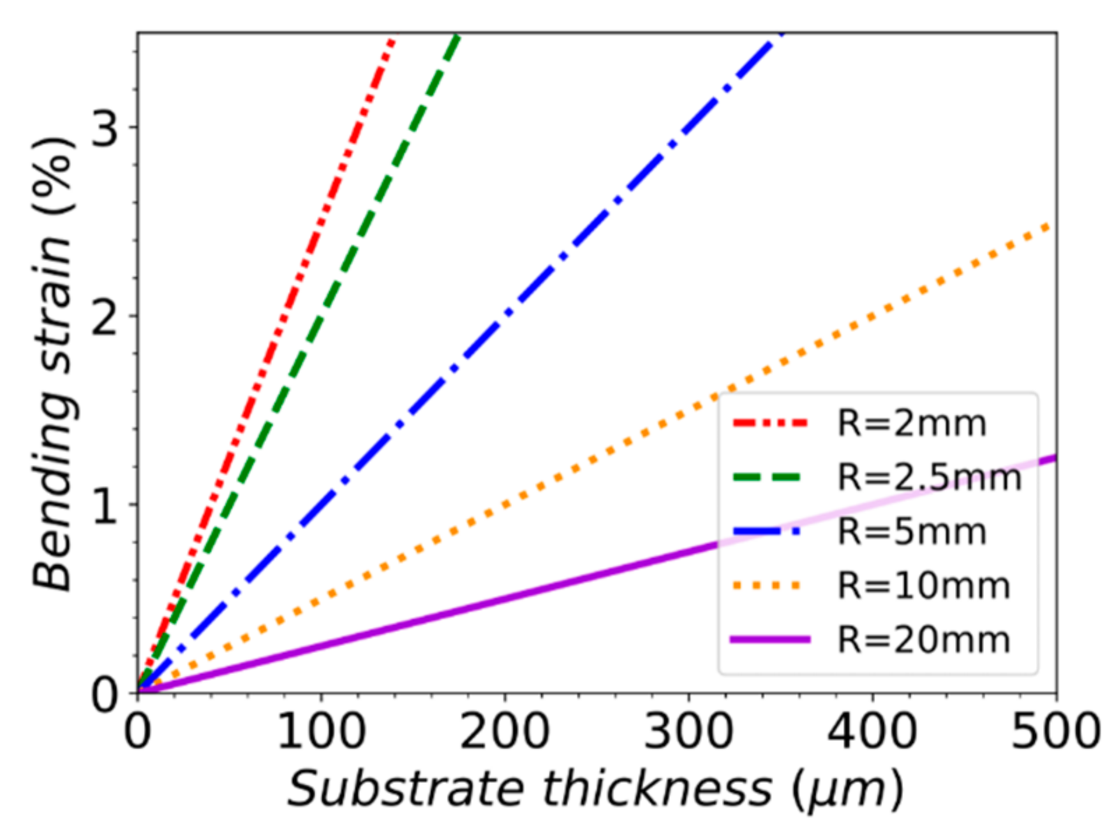
where d is equal to the substrate thickness and R is the bending radius. The proper form of Equation (1) includes the addition of the film thickness; however, in this work the film thickness is negligible for the bending strain. Simply by changing the substrate thickness or bending radius, a variety of bending strains can be achieved (Figure 1).
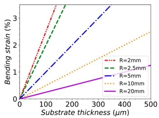
Figure 1.
Bending strains between 1%–3% can be easily achieved by tailoring the bending radius and substrate thickness (color online).
Bending is generally applied cyclically for 1000s or 100,000s of cycles. Uniaxial tensile straining, or fragmentation testing [14], can be used to determine the crack onset strain (COS), also known as the fracture strain, with the applied bending strain being set below that value. With this approach, it was initially hypothesized that the film system would be reliable without electrical failure or mechanical damage formation when bending strains below the COS were applied. However, recently, it has been demonstrated that this approach is inadequate for bending applications [15]. Thus, there is a need to fully understand and define the mechanical, electrical, or combined electro-mechanical failure, under bending conditions. Without the proper understanding of the combined electrical and mechanical impact of bending, progress to design long-lasting or even unbreakable material systems will be slow.
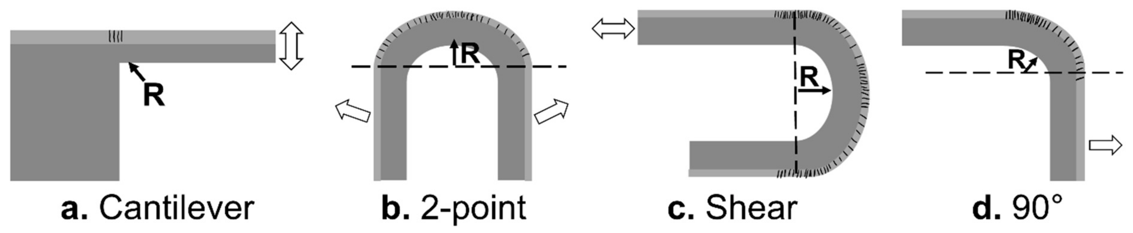
In order to study the lifetime of thin films under bending, various testing approaches have been introduced, with some techniques having electrical resistance measurements during bending [5,9,12], but not showing the continuous unbent and bent resistance as a function of bending cycles. The different approaches have brought out inconsistencies in comparing results, mostly due to where and how much damage forms and how the extent of damage impacts electrical resistance measurements. Cantilever bending (Figure 2a) [10,16,17] can be performed easily with a nanoindenter or atomic force microscope (AFM). The mechanical damage forms only in one area as a network of cracks, depending on the film architecture (i.e., number of layers, what materials, thickness). Tensile and compressive cantilever tests may depend on the setup and can quickly apply 100,000 cycles, but in situ electrical measurements or imaging of the mechanical damage evolution is challenging. The radius of bending is also dependent on the lever length. Two-point bending, on the other hand, can allow for both in situ electrical measurements and imaging, but can be much slower or even bend as a hyperbole, generating a strain gradient [11,18,19,20,21]. In this geometry (Figure 2b), only one area of damage forms that can be observed only under tensile bending. Compressive bending can be applied by turning the sample upside-down, which can make imaging through non-transparent substrates difficult, but possible. Shear bending (Figure 2c) has been heavily used, especially with support from industry [3,12,21,22]. The film system is bent between two plates at a known distance to achieve the desired R. Then, one plate moves laterally back and forth to generate the bending motion. Shear bending also allows for in situ electrical measurements during compressive bending, but in situ imaging is difficult to realize. Under shear bending, the area of damage that forms changes size as the cycles are applied, meaning the electrical resistance is due to damage forming in a continually increasing area and the sample is never in a fully relaxed state. With the area of damage increasing as well as the damage density, it is challenging to correlate the electrical resistance with the mechanical damage. One could also state that this type of loading is not true bending or folding, rather a shear loading of the system. The final bending test, and the subject of this paper, is the 90° bending (Figure 2d) [2,23]. With 90° bending, one end of the sample is clamped in grips or bent over a rod with a known radius while the other end of the sample can be free to bend or is also clamped. The repeated bending is only over one area with the area of the damage being dependent on the bending radius. Additionally, this approach could be considered the cleanest and most straightforward bending approach but is difficult for in situ imaging. Depending on the setup, in situ electrical measurements can be applied, but only intermittent imaging can quantify the mechanical damage. Bending can be applied as tensile, compressive, or a mixture of both with some configurations [2,15]. It should be noted that, as of now, cantilever bending and shear bending are not true folding tests that mimic the actual loading condition for foldable or bendable electronics, but that could change in the near-future as technology advances.

Figure 2.
Different bending configurations are available to study cyclic folding of flexible systems. Each geometry leads to different areas and amounts of mechanical damage (striped areas in a–d) that influences the electrical resistance.
With the varied ways to apply bending, it is not possible to compare the results of one method to another, mostly due to the where and how much mechanical damage forms, which impacts the electrical resistance. As has been demonstrated by others [24], there is a direct correlation with the amount of damage (generally through-thickness cracks, TTCs, or channel cracks) and the electrical resistance. However, even with the known combined electro-mechanical behavior, little has been done to properly define the failure and lifetime criteria of flexible thin films subjected to bending. The minimum that has been performed is only in situ electrical measurements. When the resistance increases a certain amount, different for different bending geometries, failure is defined as a percent increase in resistance, R, or the resistance ratio, R/R0 (with R0 being the initial resistance), without knowledge of the mechanical damage pattern or amount. This simple procedure does not consider the mechanical damage density or the resistance difference between loading (folded condition) and unloading (unfolded condition).
In this work, two 90° bending setups are compared using the same film systems and experimental procedures. The amount of mechanical damage and electrical resistances is compared to determine if the two setups apply bending in the same way. Additionally, one setup is capable of in situ resistance measurements while bending that can provide further insight into the combined electro-mechanical failure. From the results, a standardization of bending tests is suggested for the direct comparison of data with the same method and to further understand cyclic bending failure for future foldable and rollable electronics and sensors.
2. Materials and Methods
Cyclic bending tests using 90° bending in combination with electrical and optical microscopy evaluation were performed on two bending devices (Figure 3a,b). The applied tensile bending strain was 2.5% using a 2.5 mm radius grip for 10,000 cycles. The thickness of the tested films was negligible to the bending strain. A brittle 300 nm thick Mo film and a less brittle 130/50 nm Al/Mo bilayer on 125 µm thick polymer substrates were tested. To ensure a sufficient statistical measurement, 10 to 12 samples of each film type were tested per device.
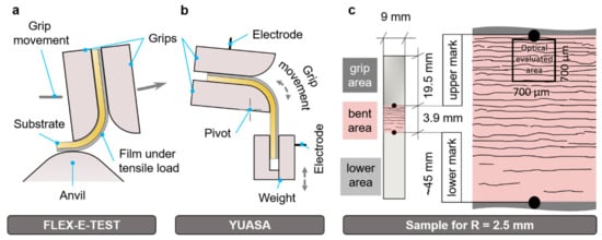
Figure 3.
Schematic of (a) the operation of the custom-built FLEX-E-TEST bending device, (b) the operation of the modified YUASA device (provided by Plansee SE), and (c) the standardized sample geometry for both devices (a,b). The enlarged picture of the bent area includes a representative schematic of the damage concentration near the grip with a black square marking the optically evaluated area.
2.1. Thin Film Deposition
Two types of thin film architectures were tested, (1) a 300 nm thick Mo film and (2) a 130/50 nm thick Al/Mo bilayer, both supported by a 125 µm thick polyimide (PI) substrate (Upilex-S). Both were deposited using an industrial-scale magnetron sputter system (FHR.Line.600-V) equipped with a planar Al target (600 × 125 mm, 99.9995% purity, FHR Anlagenbau, Ottendorf-Okrill, Germany) and a rotary Mo target (Ø 125 × 600 mm, 99.97% purity, Plansee, Reute, Austria). Prior to deposition, the PI was pre-cut to 70 × 9 mm strips using a Cricut Explore Air 2 and ultrasonically cleaned in an ethanol bath for 10 min. After mounting in the deposition chamber, the substrates were plasma-etched for 380 s at 0.8 kW under 0.34 Pa (180 sccm Ar flow rate). A total of 30 samples were deposited at the same time using the same deposition conditions. The base pressure for the bilayer in the deposition chamber was 2 × 10⁻⁶ Pa. The bilayers were deposited with an Ar flow rate of 300 sccm, corresponding to a pressure of 0.52 Pa. Direct-current powers of 4 kW for the Mo and 3.5 kW for the Al target were used, yielding respective deposition rates of 5.26 nm/s for Mo and 3.57 nm/s for Al. The deposition time of the 50 nm thick Mo and 130 nm thick Al layer were, respectively, 9.5 s and 35 s in static deposition mode. For the deposition of the 300 nm thick Mo film, the same Ar flow rate was used, but with a direct current of 2 kW and 154 s deposition time. During deposition, the PI substrates were held at ground potential, without additional external heating.
2.2. Monotonic Tensile Testing
As an initial characterization of the two film architectures, in situ fragmentation testing [25] with resistance measurements on an MTS Tytron 250 to a maximum applied strain of 10% was performed. The COS was determined as a 10% increase in the R/R0 (resistance ratio) from the constant volume approximation theory [26]. Three samples of each film system were tested and the average COS and saturation crack densities were evaluated. The average COS of the 300 nm Mo film was 1% with the average saturation crack density being 1/λ = 0.12 ± 0.1 µm−1 (λ = 8.3 ± 0.5 µm). The Al/Mo film system had a higher COS at 4.3% and a similar average saturation crack density 1/λ = 0.17 ± 0.01 µm−1 (λ = 6.0 ± 0.4 µm). The 300 nm Mo film COS was below the applied 2.5% bending strain, while the COS of the Al/Mo film architecture was almost twice the applied bending strain.
2.3. Bending Tests
The FLEX-E-TEST is a custom-built research instrument for cyclic bending loads [2]. The samples are bent against a grip with a defined exchangeable radius during cyclic rotation of the grip. The sample itself acts as the lever, while the grip passes repeatedly over an anvil, as schematically shown in Figure 3a. The rotation frequency of the FLEX-E-TEST is 1 Hz and there is some spring back after passing the anvil. The grip allows an easy insertion and removal of the sample with high accuracy and precision (less than 0.5 mm error). The advantage of the FLEX-E-TEST is that multiple grips with samples can be cycled simultaneously. However, in situ resistance measurements are not possible in this mode/setup. Due to the principle of the FLEX-E-TEST, it should be noted that the actual bending and unbending action lasts for approximately an eighth of a cycle, yielding an estimated strain rate of the FLEX-E-TEST, , of 0.2 s−1, according to the calculation , where Δt is the duration of one bending event (0.125 s).
The commercially available endurance test system from YUASA (YUASA System Co., LTD., Okayama, Japan), which herein is referred to as the YUASA test, is an instrument that allows different configurations (bending, torsion, folding, rolling, tension). For this study, the original bending configuration with a clamp, round bars, and a weight was customized with a grip similar to the FLEX-E-TEST to ensure that the location of the bent area was well defined and comparable (Figure 3b). Otherwise, the evolution of the damage of the YUASA could not be compared to that of the FLEX-E-TEST. To ensure repeatability of the sample position, holes were added to the grip and weight using needles to align the sample during the mounting and dismounting for intermittent characterization. Furthermore, the grip was electrically isolated and pins for electrical measurements were added to the grip and the weight (168 g, Cu), allowing in situ electrical resistance measurements in the four-point probe configuration during cyclic bending. For the in situ resistance measurements and a stable bending process, a bending frequency of 0.5 Hz was chosen. In comparison to the FLEX-E-TEST, the YUASA test yields a strain rate = 0.0125 s−1 (εb = 0.025, Δt = 2 s), i.e., a 16 times lower strain rate with little to no spring back.
2.4. Intermittent Measurements
The test procedure for both bending devices was the same. At specified cycle numbers (0, 25, 50, 100, 1000, and 10,000 cycles), intermittent measurements of the electrical resistance using the four-point probe configuration and mechanical damage with confocal laser scanning microscopy (CLSM, Olympus LEXT 4100) imaging were performed. During the measurements, the samples were dismounted and in their flat state. For the electrical resistance measurements, the resistance of the bent area was measured only. The sample was put under two flat grips with electrodes separated by a distance of 3.9 mm (Figure 3c). For comparable measurements, the load of the grips was controlled with a torque wrench (2 N). The optically evaluated area was 700 × 700 µm and always taken near the upper grip (Figure 3c). It should be noted that as the schematic in Figure 3c and the real example in Figure 4 show, the damage from repeated bending was inhomogeneous and the optically evaluated area represented the area with the highest damage. However, the resistance measurements represented a global average of the bent area [15]. The laser intensity images were evaluated with a line intercept method using five-line profiles per image perpendicular to the bending axis to quantify the linear crack density. After 10,000 bending cycles, scanning electron microscopy (SEM, Zeiss LEO 1525, Oberkochen, Germany) and focused ion beam (FIB, Zeiss Leo 1540XB workstation, Oberkochen, Germany) cross-sections were prepared for further investigations to gain insights into the damage mechanisms.
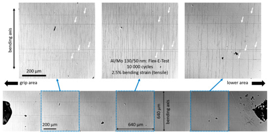
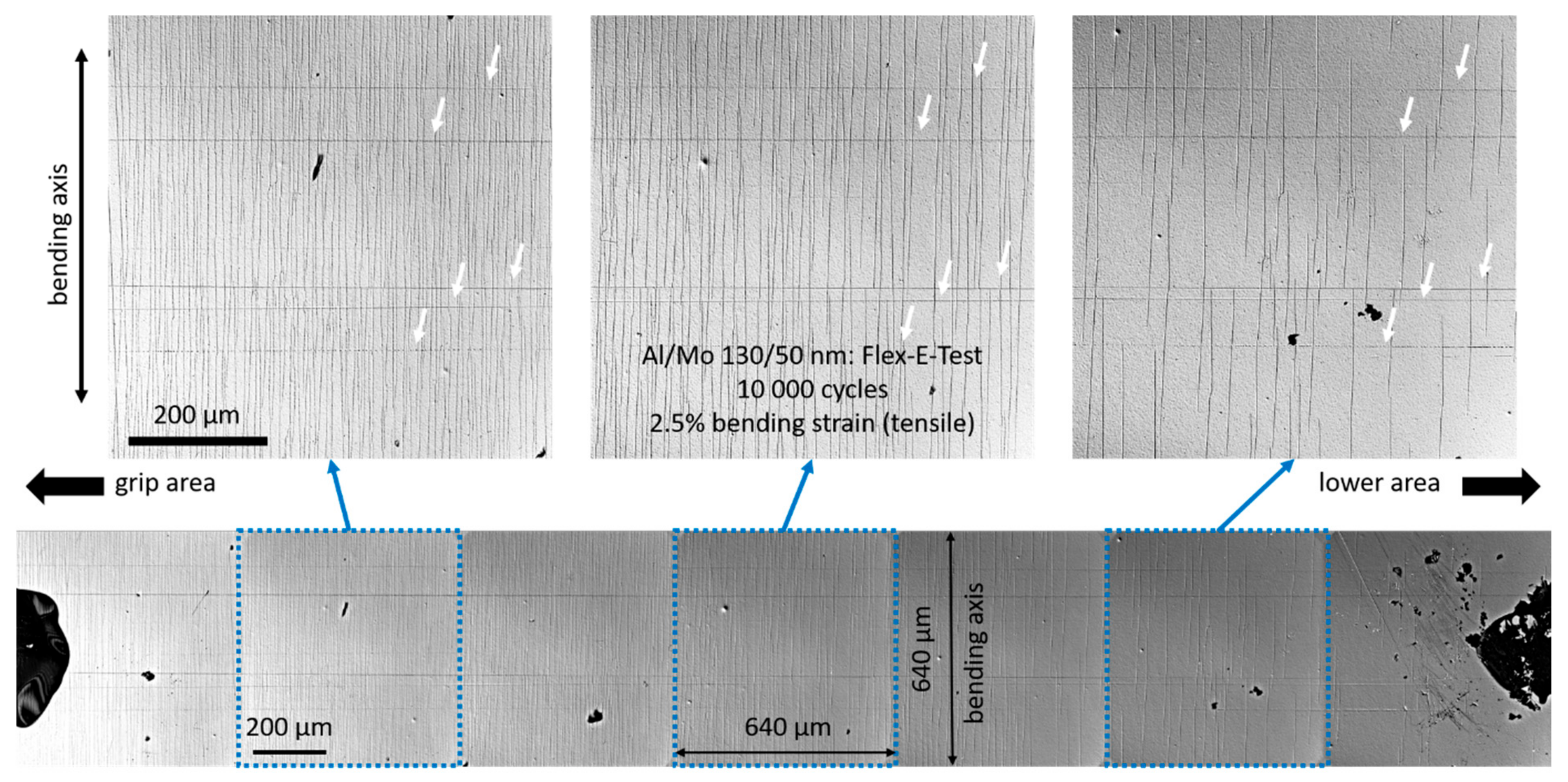
Figure 4.
CLSM laser intensity images stitched together to illustrate the inhomogeneous damage that forms during bending of the Al/Mo bilayer tested in the FLEX-E-TEST after 10,000 bending cycles of 2.5% applied tensile bending strain. Near the grip, the crack density has saturated; in the middle, cracks could still form; and in the lower area, cracks are still forming. The white arrows indicate substrate scratches that do not impact the electrical conductivity of the film in this orientation (parallel to cracking direction).
3. Results
In order to properly compare the two devices and samples, a few definitions are necessary. The term “mechanical damage” is used to describe through-thickness cracks (TTCs) and localized thinning (also called necks or necking). TTCs and localized thinning can be indistinguishable in laser intensity images, explaining why both were used in the definition. In the two film systems studied, however, mostly TTCs formed due to cyclic bending. In the laser intensity images produced with CLSM, necks and TTCs are identified as black lines (see Figure 4). As shown later with FIB cross-sections, all of the damage produced in both film systems is TTCs. For the Mo film systems, 12 samples were tested and 10 samples of the Al/Mo film system were tested on each bending setup. All samples and data are shown to demonstrate the reproducibility of the same film system as well as the statistical significance of the testing methods.
3.1. Intermittent Bending Results in the Relaxed State
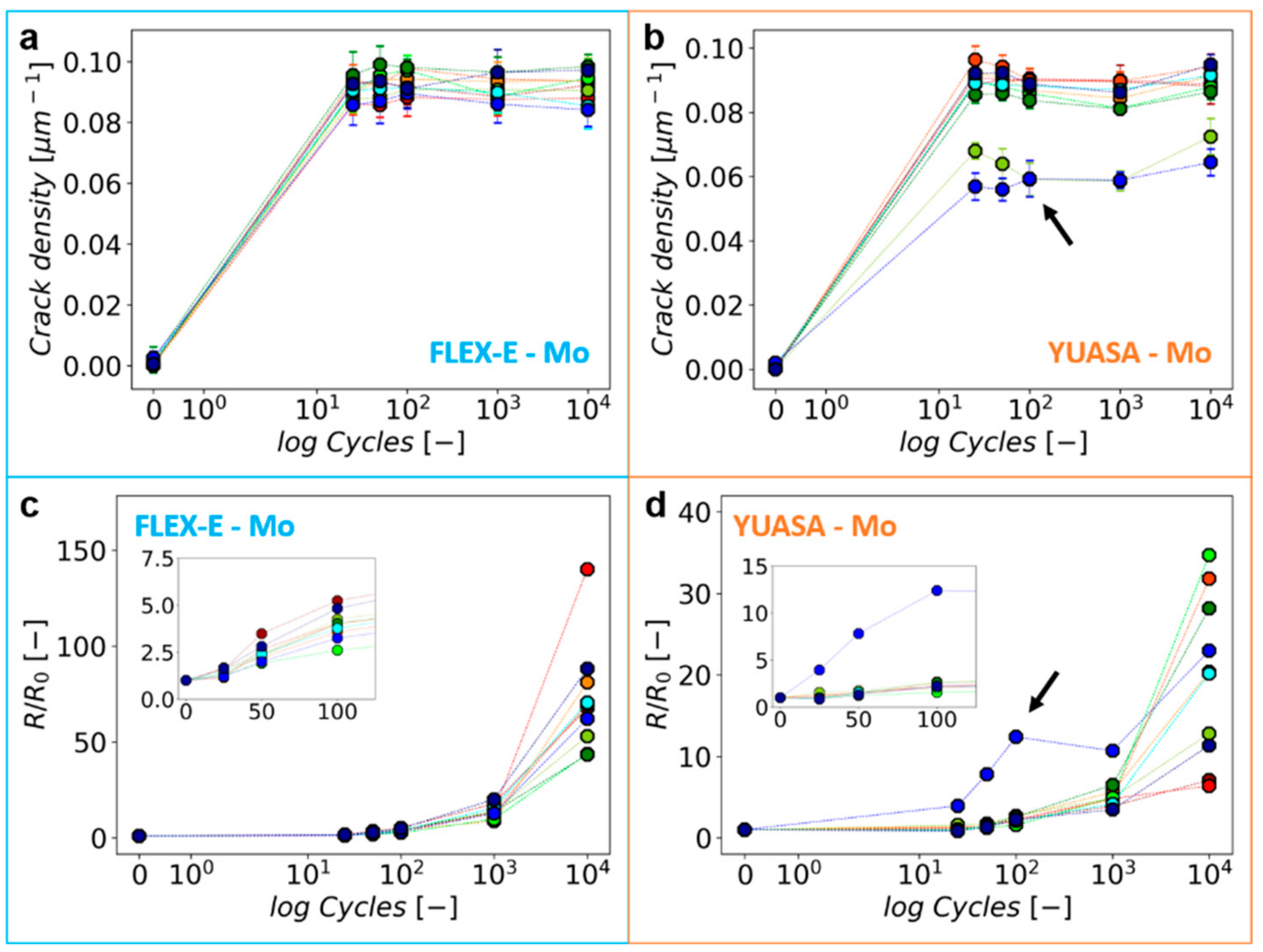
After 25 bending cycles of the single Mo films on polyimide, samples tested on both FLEX-E-TEST and YUASA reach a plateau in the crack density at similar values (Figure 5a,b). The mechanical damage and electrical resistance data are presented similarly to other work [15,27] where in situ resistance measurements were not available. This is not surprising, as the crack density is measured near the grip where damage occurs first; thus, it would reach saturation before the bottom of the damaged area. The FLEX-E-TEST appears to have more uniform statistics with all samples clustering together, while the samples tested on the YUASA have two outliers. Both methods achieve similar damage results for this brittle film system with the average crack density after 10,000 cycles being 1/λ = 0.092 ± 0.002 µm−1 on the FLEX-E-TEST and 1/λ = 0.086 ± 0.003 µm−1 on the YUASA. The resistance data, shown in Figure 5c,d, have a large difference in the scale of the y-axes. FLEX-E-TEST R/R0 does not significantly increase until after 1000 cycles, and after 10,000 cycles, the R/R0 values are approximately between 50 and 150 (Figure 5c). The YUASA samples also show an increase in resistance after about 1000 cycles; however, after 10,000 cycles, the end R/R0 is much lower, only ranging between 5 and 35 (Figure 5d). Of note is that one of the two outlying samples in Figure 5b (marked with arrow) shows average electrical behavior and the other outlier has slightly higher values compared to the other samples clustered together (arrow in Figure 5d). Further examination of the sample found that a scratch oriented in the same direction as the cracks was present from the beginning of the experiments, which could be the reason for the different behavior of this sample. Figure 5 also points out the need to test many samples. If only three samples were tested, erroneous average behavior could be reported. Additionally, Figure 5 shows that the resistance results could be influenced by the speed of the testing since the samples tested with the FLEX-E-TEST have a much higher R/R0 range and most likely infer more damage due to spring back of the sample.
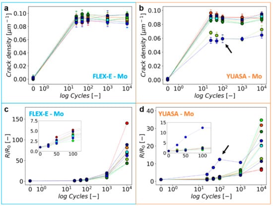
Figure 5.
Results of the 300 nm thick Mo films under 2.5% bending strain in semi-logarithmic scale. In the top row, the evolution of crack density for (a) FLEX-E-TEST and (b) YUASA is presented. In the bottom row, the evolution of normalized resistance for (c) FLEX-E-TEST and (d) YUASA is presented. The insets in (c,d) show a linear scaled zoom of the first 100 cycles. The measurements were performed during designated breaks on the flat sample. The lines between data points only guide the eye and have no mathematical or statistical meaning (color online).
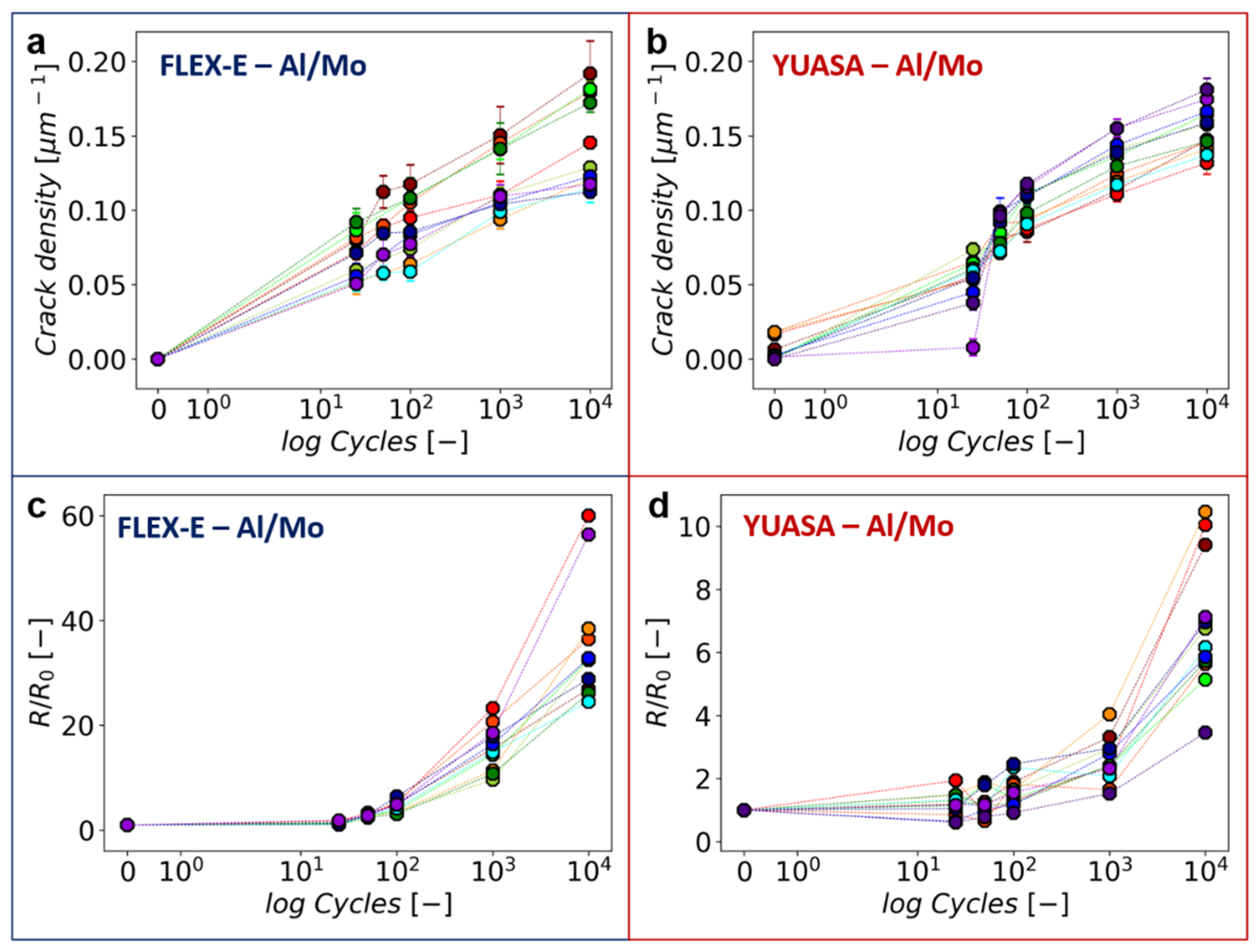
The Al/Mo bilayers demonstrate a very different behavior compared to the single Mo film during intermittent bending. Starting again with the samples tested in the FLEX-E-TEST, all 10 samples illustrate a steady increase in the damage density with no saturation or plateau (Figure 6a, note the semi-logarithmic scale). The spread of the samples is quite large with the final damage density ranging from 0.1 µm−1 to almost 0.2 µm−1 compared to the single Mo film. There also appears to be two clusters of sample behavior after 10,000 cycles. All of the samples tested in the YUASA have a jump between 25 and 50 cycles in the damage density data (Figure 6b). Currently, it is not known why or how this jump manifests in the mechanical data, but the fact that it occurs for all 10 samples tested suggests it could be an artifact from the testing apparatus, but not the intermittent testing method, since the same jump was not observed in any of the FLEX-E-TEST experiments. After 10,000 bending cycles, the damage density of the YUASA samples is slightly lower than the FLEX-E-TEST with values between 0.12 µm−1 and 0.18 µm−1. The higher damage density in the Al/Mo bilayers means that the average damage spacing is slightly smaller compared to the single Mo layers. This result is logical due to the fact that the Al/Mo bilayer total thickness is less than that of the single, 300 nm Mo film system. The electrical resistance increases at a similar rate in the Al/Mo bilayers as in the single Mo film; however, the mechanical damage in the Al/Mo system causes the resistance ratio to increase between 50 and 100 bending cycles (Figure 6c,d). Again, the reader should note the different scales on the y-axes. FLEX-E-TEST samples (Figure 6c) all follow the same trend up to the maximum applied cycles, with two outlying samples. The YUASA samples (Figure 6d) also have the increasing trend, but the individual sample behavior can be observed more easily due to the overall lower R/R0 increase. Again, the significant difference of R/R0 in the FLEX-E-TEST and YUASA could be due to the speed of the testing and the additional spring back the FLEX-E-TEST samples are subjected to.
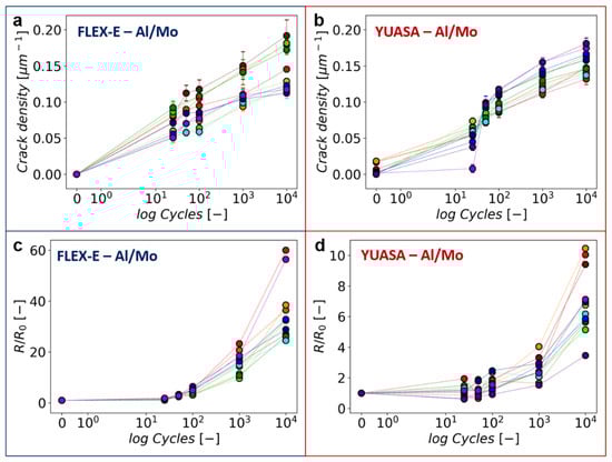
Figure 6.
Results of the Al/Mo bilayers with 130/50 nm thickness under 2.5% bending strain in semi-logarithmic scale. In the top row, the evolution of crack density for (a) FLEX-E-TEST and (b) YUASA is presented. In the bottom row, the evolution of normalized resistance for (c) FLEX-E-TEST and (d) YUASA is presented. The measurements were performed during designated breaks on the flat samples. The lines between data points only guide the eye and have no mathematical or statistical meaning (color online).
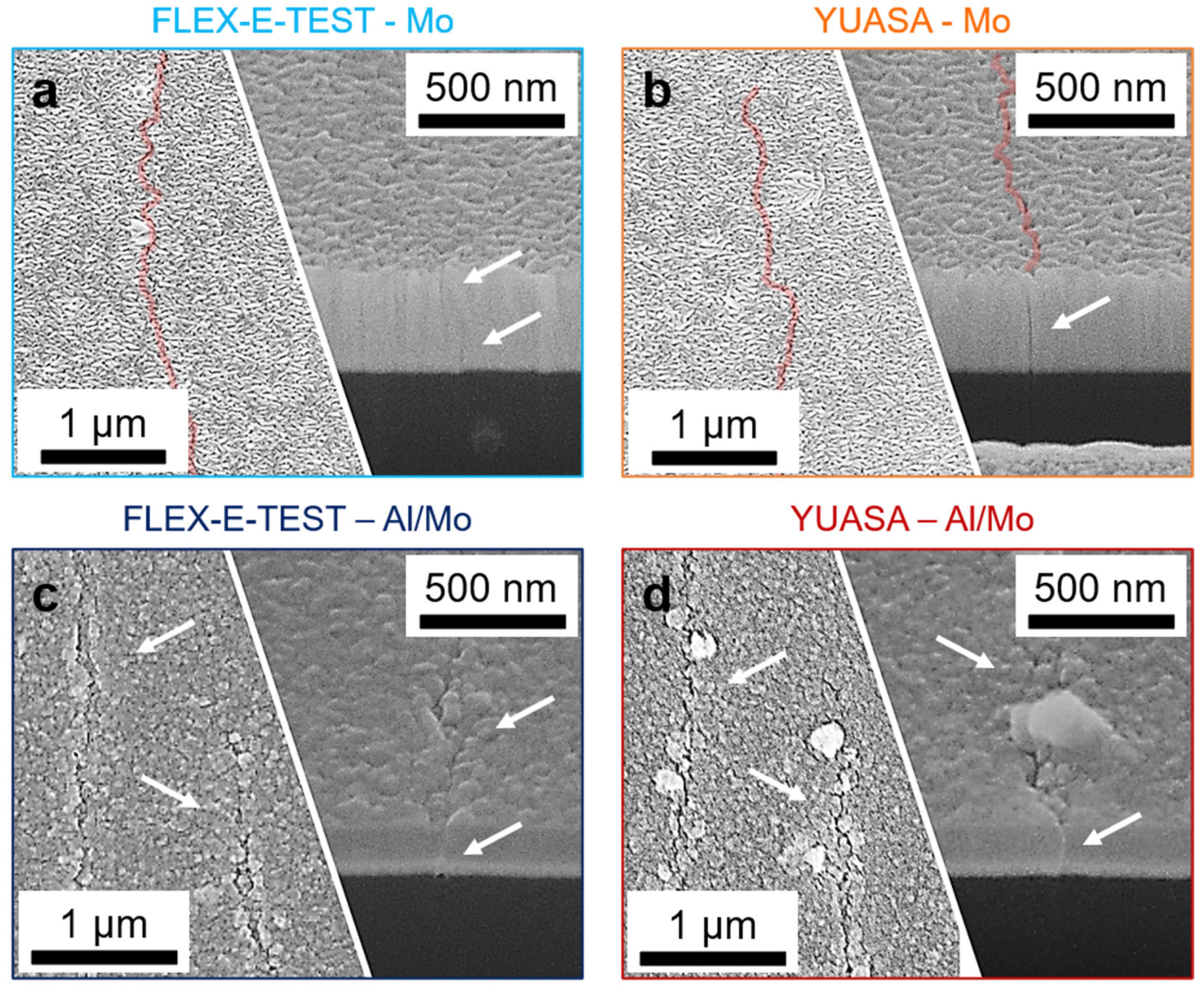
SEM images and FIB cross-sections illustrate that TTCs formed in all samples (Figure 7) after 10,000 bending cycles. The Mo film surface is quite rough and, due to the samples lying flat, the closed cracks are difficult to observe (Figure 7a,b). Nonetheless, cracks clearly travel through the film thickness and are the cause for the increase in electrical resistance. Similar mechanical damage in the form of TTCs is observed in the Al/Mo bilayers (Figure 7c,d). Again, samples are imaged in the flat and relaxed configuration where cracks are allowed to reconnect or bridge [28]. On the surface of the Al film, the TTCs are accompanied by extrusions of material, indicative of cyclic loading [27]. In the cross-sections, cracks in the Mo layer occur at the same position as the cracks in the Al layer. In Al/Mo bilayers, this behavior is known and well understood [15,29].
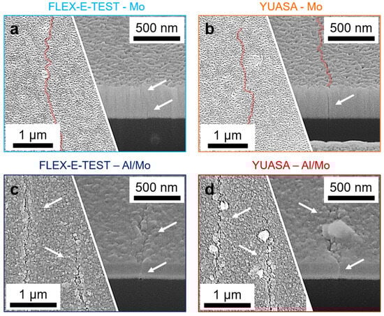
Figure 7.
Representative SEM micrographs of the Mo (a,b) and Al/Mo (c,d) films after 10,000 bending cycles, tested with the FLEX-E-TEST (a,c) and the YUASA test (b,d). Surface images are on the left side and the cross-sectional area is displayed on the right side. Cracks are marked by red highlights and white arrows (color online).
3.2. In Situ Bending Results
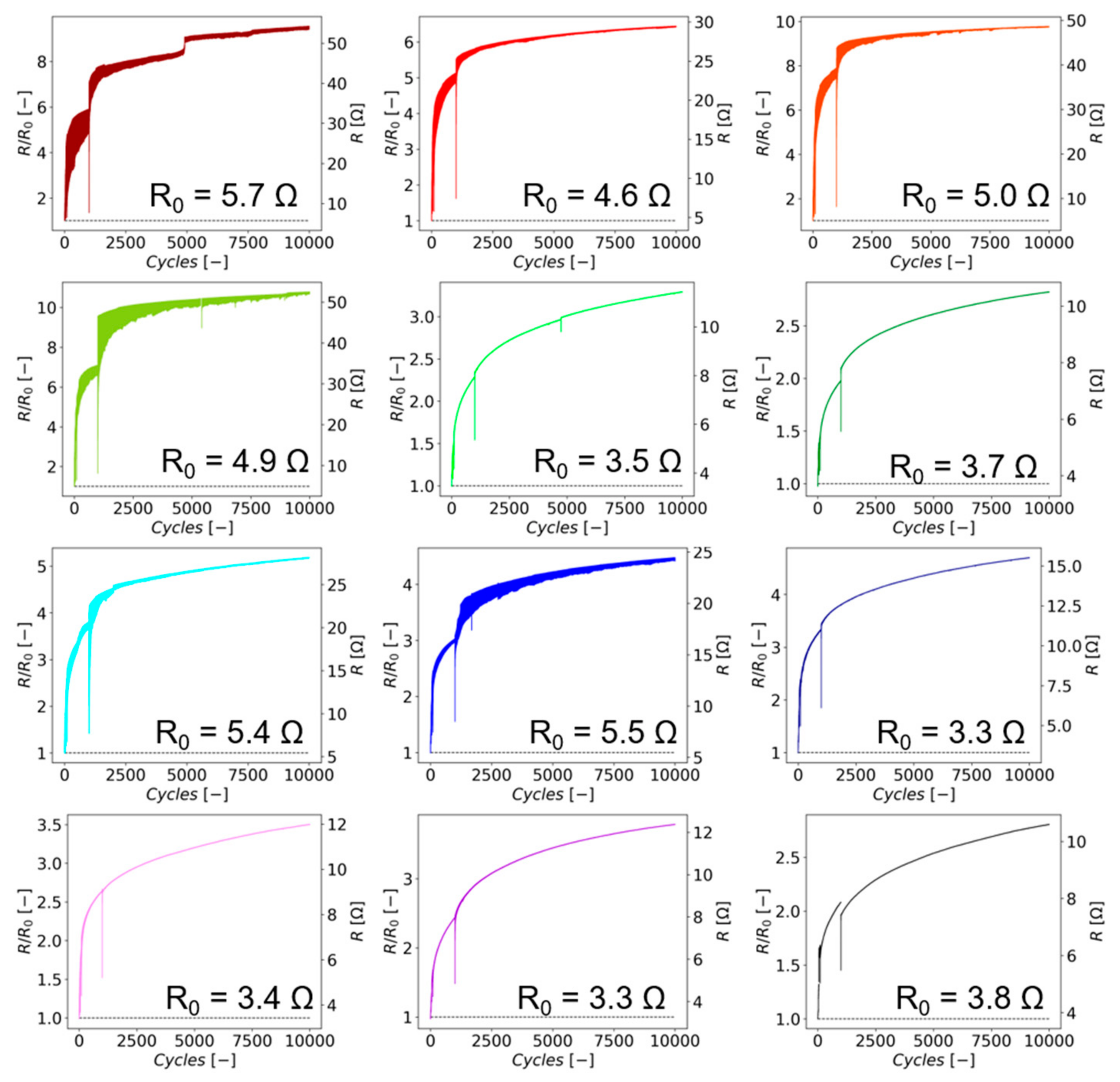
Since the YUASA system is capable of measuring the resistance in situ during bending, a closer look at what can be learned from these data was performed. Figure 8 contains the in situ resistance data for every Mo/PI sample tested in the form of R/R0 (left y-axis) and R (right y-axis). What might be surprising is that almost every sample has a different initial resistance and electrical response to the bending. No two samples behave the same even though all samples were pre-cut to avoid film cracking due to cutting from one large piece and were made at the same time in the same deposition system during the same deposition run. The only difference is the position in the chamber where each sample originated and could be a source for inhomogeneous film thicknesses. However, the film thickness distribution on samples positioned on different sites of the 600 mm × 600 mm substrate carrier was thoroughly investigated [30], and only the center of the deposition area with a manufacturer-certified ±5% thickness accuracy was utilized to achieve as close to uniform film thickness as possible. The graphs in Figure 8 contain all of the data obtained the intermittent testing, and discrepancies in the data (jumps or outlying data points) sometimes occur due to combining the data (from combining the data between cycles). Another source of the jumps in the resistance data could be from the viscoelastic recovery in the PI during intermittent measurements. Additionally, the data shown in each graph are the electrical response during loading (maximum values, peaks) and unloading (minimum values, valleys). The maximum values (peaks) are when the sample is in the folded condition with open cracks and the minimum values (valleys) are when the sample is in the unfolded position with closed cracks. The cracks in this condition can still conduct as demonstrated by Gebhart et al. [28].
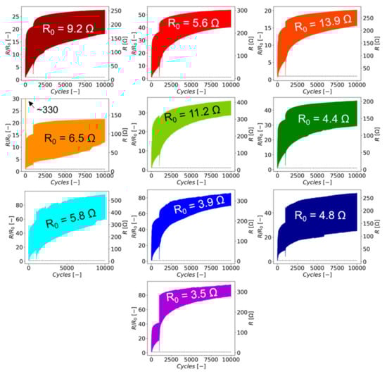
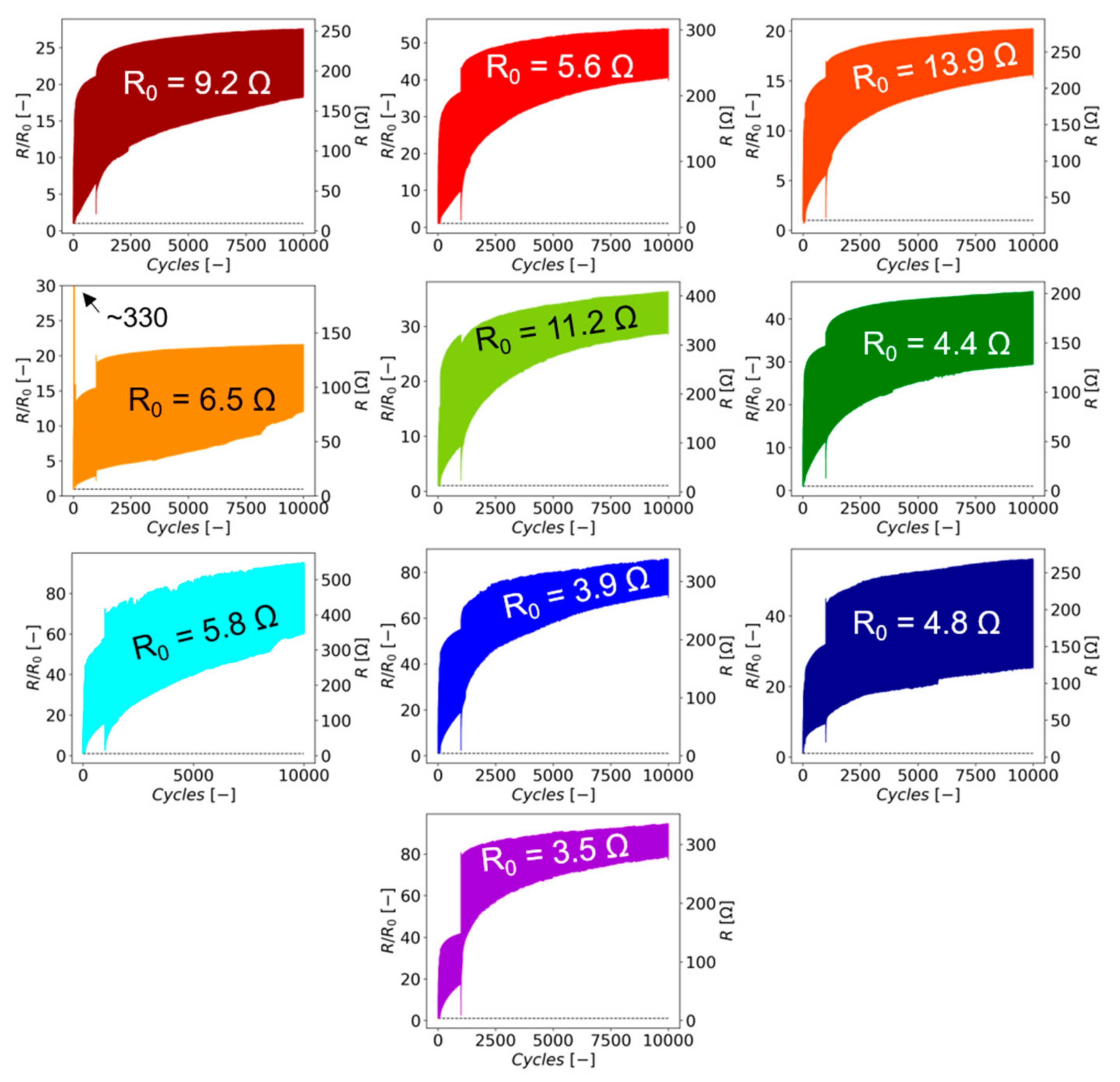
Figure 8.
Comparison of the YUASA in situ resistance of the individual Mo films during intermittent cyclic testing with stops after 25, 50, 100, 1000, and 10,000 cycles. R0 denotes the initial resistance measured at 0 cycles. The dashed black line marks the start value (for R/R0 = 1 and for R = R0). Note that all y-scales are different (color online).
In each graph, the initial R0 is stated, ranging from 3.5 to 13.9 Ω, and after cycling, the final resistances are between 75 and 550 Ω. Some similarities of samples are as follows: (1) the immediate increase from the initial resistance to above 10 Ω for the first 25–50 cycles, (2) a bending over of the resistances between 100 and 1000 cycles, and (3) somewhat of a plateau of the maximum and/or minimum resistance values by the time 10,000 cycles are achieved. The initial resistance increase indicates the formation of long TTCs since the COS of the Mo film system has been overcome after one bending cycle. Many of the samples appear to reach a plateau in the electrical response (maximum or minimum value) when continuously measured. For some samples, the amplitudes between the maximum and minimum resistance values are quite large and could indicate that the sample had large pre-existing defects or substrate scratches (especially oriented perpendicular to the crack direction, see Figure 4) that heavily influence the measured electrical resistance by initiating long cracks. These defects could have been activated in the first cycle up to 25 cycles. Other samples have a lower amplitude and may not be influenced by possible pre-existing substrate defects. The size of the resistance amplitude most likely indicates collective crack extension (growth) and resistance recovery with the straightening of the samples.
Resistance provides information about the global TTC extension in the measured area. The initial large increase in resistance should be an indication of immediate failure since the increase is over 20% of the initial resistance for every sample, which can be defined as electrical failure criteria [31,32]. The knowledge that after only 25 cycles, the crack density of the 300 nm Mo films has saturated near the grip should be clear signs for failure. Additionally, the in situ resistance does indicate an electrical saturation in most samples either with the maximum or minimum relative resistance values. The more important electrical response is the minimum resistance in the straight or relaxed condition (unfolded) as this is the more likely position of a device in operation (opened rather than folded). It is thus the electrical resistance that should be considered in terms of failure.
In comparison to the single Mo films, the Al/Mo bilayers have a completely different in situ response. Again, the data in Figure 9 are the combined in situ resistances measured during the intermittent tests, the jumps in data account for the remounting of the sample, and all samples were produced within the same deposition run with only the position of the sample in the chamber varying. The initial resistances, R0, have a smaller range from 3.3 Ω to 5.7 Ω compared to single Mo films and could be due to the fact Al is a more conductive metal than Mo. Recall that the damage density was observed to continuously increase (Figure 6b) from the intermittent results. The in situ R/R0 indicated that the TTCs or at least a critical amount of mechanical damage to alter the electrical resistance continuously occurs. With each bending cycle, the damage, either localized necks or TTCs, extends in the plane of the film or through the two layers. The resistance increase is much slower compared to the Mo/PI because Al allows for plasticity (Figure 7c,d) that will influence how damage, or cracks, propagate and, thus, how the resistance will respond to the damage. Even at 10,000 cycles, a resistance plateau is not achieved, indicating that there are still pathways for current to flow and cracks or necks can continue to form or extend [33]. Moreover, recall that a gradient of damage is still present that will also have an influence (Figure 3c and Figure 4).

Figure 9.
Comparison of the YUASA in situ resistance of the individual Al/Mo films during intermittent cyclic testing with stops after 25, 50, 100, 1000, and 10,000 cycles. R0 denotes the initial resistance measured at 0 cycles. The dashed black line marks the start value (for R/R0 = 1 and for R = R0). Note the different y-scales (color online).
If the 20% increase is considered as the electrical failure criteria [12,31,32,34], then after only 25 cycles about half the YUASA samples (Figure 9) would be considered failed, while for the other half of the samples, the 20% increase occurs between 100 and 1000 cycles. The difference to the single Mo film system is that the crack or damage density is not at a saturation point after 25 cycles, nor at a saturation after 10,000 bending cycles in the Al/Mo bilayers. In a more ductile film system, TTCs take longer to form and can also be slower to extend across the sample width due to crack growth mechanisms. TTCs still form even though the applied bending strain was lower than the measured COS of the film system. While for the Mo system (COS = 1.0%), fracture is expected at the first bending cycle (bending strain = 2.5%), for the Al/Mo system (COS = 4.3%), damage takes more time to accumulate and saturate. A more thorough examination of the in situ resistance data is performed in the discussion.
4. Discussion
A comparison of the average electrical response and mechanical damage of both film architectures and the different bending tests (FLEX-E-TEST, YUASA) was made. The in situ resistance data were analyzed qualitatively by examining the sine curves created by the bending. Such an analysis of the resistance data has been shown to have the ability to distinguish when TTC formation has occurred in Au films [28].
4.1. Intermittent Bending
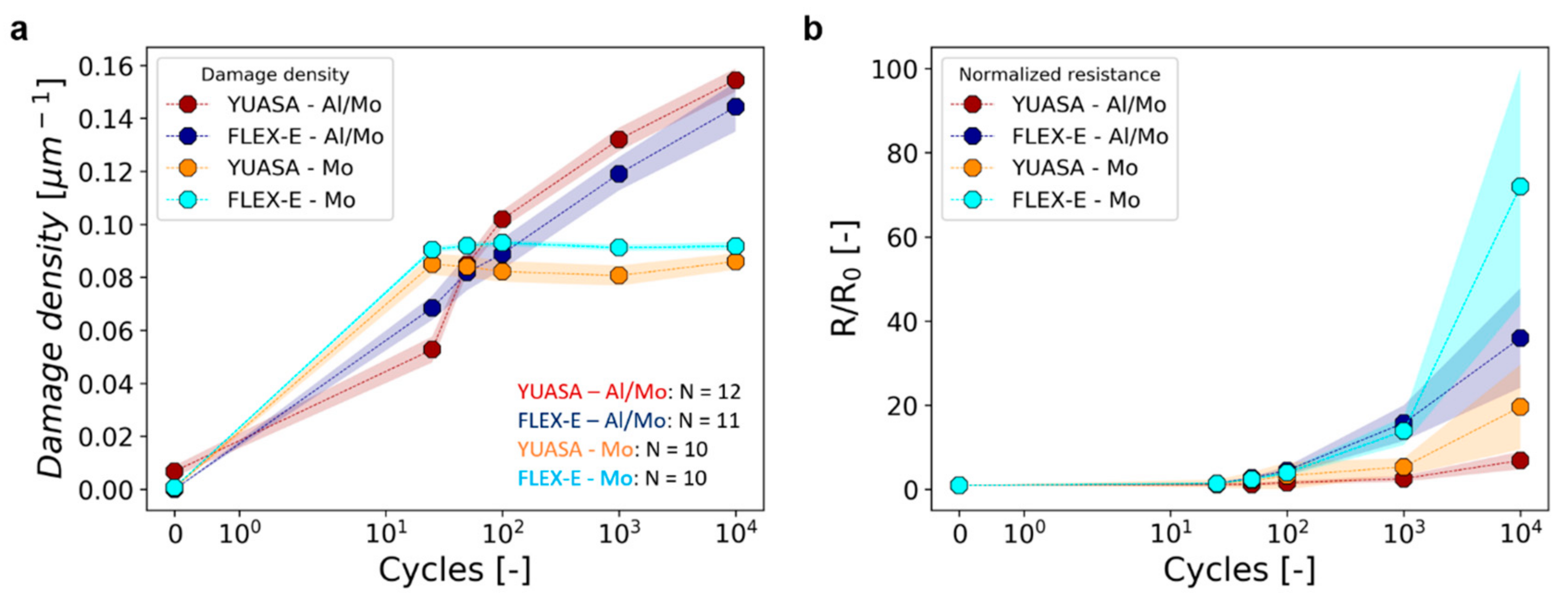
The measured damage density from both bending methods and film systems is very similar (Figure 10a). For both film systems, the evolution of the mechanical damage follows the same trend with very similar measured values for damage density from the CLSM images. After 10,000 bending cycles, the crack densities are slightly lower than for the uniaxial straining of both film systems (Mo: 0.12 µm−1, Al/Mo: 0.17 µm−1). The relative resistance ratios, however, are quite different (Figure 10b). The FLEX-E-TEST values are significantly higher than the YUASA values for the same film system. One possible reason for the difference in resistance but not in the mechanical damage (crack density) is that the TTCs are shorter in the Al/Mo samples tested on the YUASA. Shorter cracks would be due to a slower bending rate and no spring back with the YUASA samples. The additional spring back applies additional forces to the film, causing additional crack extension, both through the film thickness and in the plane of the film. A close examination of Figure 11 comparing SEM images from Al/Mo tested on the FLEX-E-TEST and YUASA qualitatively reveals that the crack lengths are shorter on the YUASA samples; thus, the measured resistances are lower. A similar comparison could not be made on the Mo films, due the high surface roughness (Figure 7a,b). This concept is quite important: for the electrical resistance, it does not matter how many TTCs are present, as quantified with the crack density, due to bending (or stretching), it depends more on the average or effective crack lengths of the TTCs that hinder electrical conduction [24]. Long TTCs without bridges increase the resistance significantly faster than short TTCs that allow for bridging [28].

Figure 10.
Comparison of (a) average damage density and (b) average normalized resistance with the standard error as filled area. The lines connecting the points are guides for the eyes and have no mathematical or statistical meaning. Note the logarithmic scale for the cycles (color online).
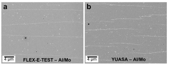
Figure 11.
SEM micrographs of representative Al/Mo samples after 10,000 bending cycles performed on the (a) FLEX-E-TEST and (b) YUASA demonstrate that the mechanical damage on the FLEX-E-TEST has long cracks, while on the YUASA, the damage has many shorter cracks that are not connected.
What can be definitively said about the bending of the Mo/PI and Al/Mo/PI film systems is that brittle systems will reach a mechanical damage density saturation after only a few cycles, while more ductile film systems may need 100,000 cycles to reach a damage density saturation. What is also of note is that the relative resistance ratios also do not saturate, even after 10,000 cycles, and when only the damaged area is measured, pathways for electrical current to flow could still be present due to the damage gradient [27,33]. Without electrical saturation, it is difficult to use resistance as a failure criterion since it is always increasing. Additionally, by testing 10 to 12 samples for each method, it can easily be observed that testing only 1 or 2 samples is not sufficient to properly evaluate the average electro-mechanical behavior of a film system. Even when all other parameters are kept constant, such as using pre-cut substrates and films deposited in the same deposition run to ensure the exact same sample shape, there are still variables, especially substrate scratches, that cannot be easily accounted for or avoided. The experiments presented here also illustrate that the testing method can also bring out slightly different results, such as the speed of the bending between the FLEX-E-TEST and YUASA. While the speed of the FLEX-E-TEST can be reduced, the spring back is much more challenging to control. If the substrate thickness was reduced, the spring back will most likely be reduced due to the samples being lighter and the presence of air resistance; however, similar bending strains could not be reached as with a thicker substrate (Figure 1).
The ability to measure the electrical resistance of a thin film during stretching or bending can provide a wealth of new information about the mechanical damage. Oddly enough, these data are generally not analyzed much past what is presented in Figure 8 and Figure 9. For the first cycle, the resistance immediately increases and continues to increase for the first 20–50 cycles. One could apply the 20%–25% relative resistance ratio increase as failure criteria for devices [31,32] and determine that the film systems failed after 1 or 2 cycles for the single Mo films and after fewer than 30 cycles in the Al/Mo bilayers. In the first 25 cycles, the mechanical damage is large enough to significantly influence the electrical behavior. The damage could be long TTCs that travel across the entire width of the sample or a critical density of shorter TTCs that cause the resistance to markedly increase. Within the first 25 cycles, most of the damage (cracking) occurs in both film systems and further cycling only increases the crack lengths further away from the measurement area or crack openings of existing cracks. For the Al/Mo bilayers, the damage is incremental with a continuous increase in the damage density (Figure 10a) and R/R0 (Figure 10b).
4.2. In Situ Resistance during Bending
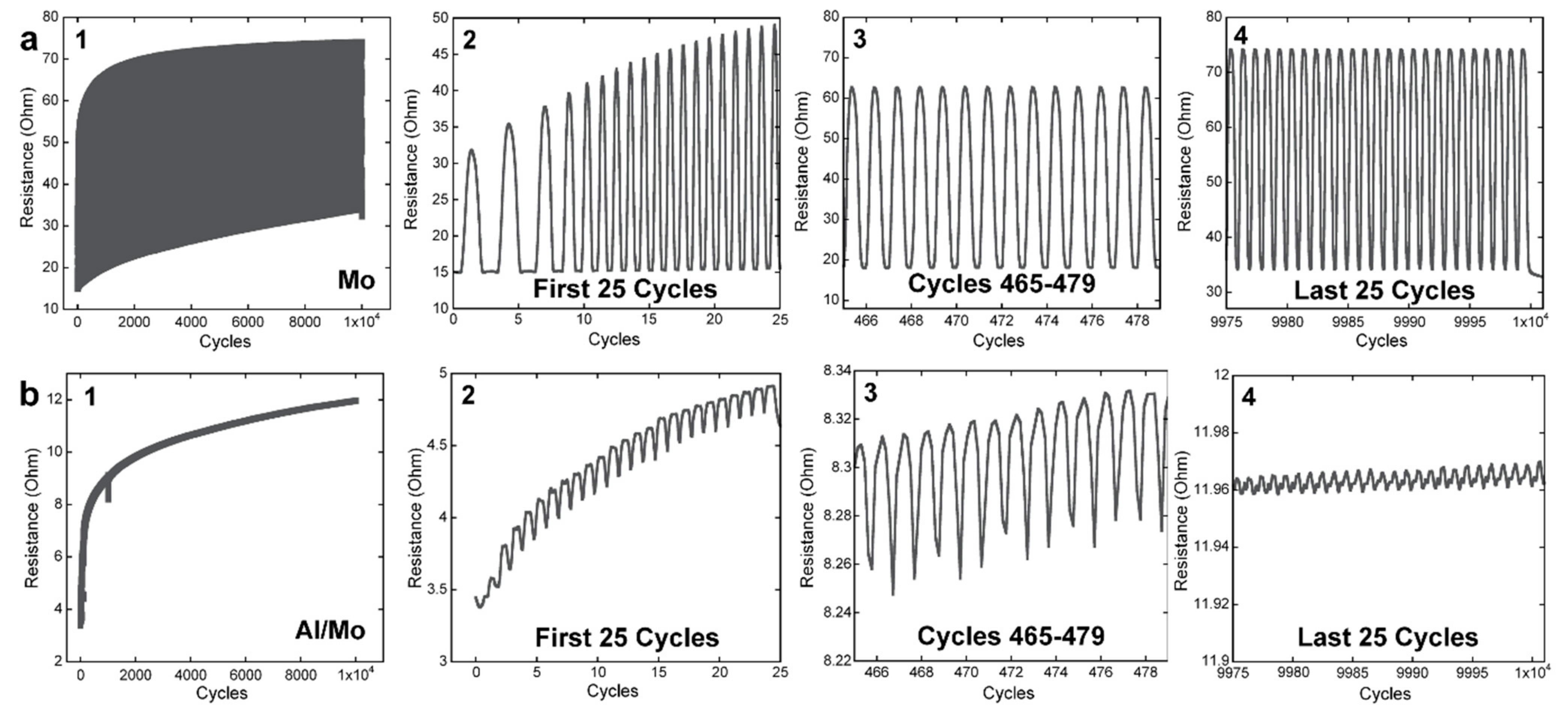
Upon much closer inspection of the in situ resistance data, especially after 100s or 1000s of cycles, the sine function of the data changes. An additional experiment on the YUASA of the Mo film was performed without intermittent characterization to better observe the electrical resistance evolution (Figure 12(a1)). The shape of resistance data as a function of cycles is reminiscent of the Au/Cr system [28] and a printed Ag film [35] that were subjected to uniaxial cyclic tensile straining. During the first 25 bending cycles (Figure 12(a2)), the Mo film experiences an immediate increase in the resistance amplitude that remains large for the entirety of the experiment. The first cycles also show evidence of flat minimum (unfolded) values that are known to be crack bridging that recovers conductivity [28,35]. These minimum values quickly increase with further cycling (Figure 12(a3,a4)). The shape of the resistance sine curves remains uniform with large amplitude. After 465 cycles (Figure 12(a3)), the average minimum resistance is about 27% higher than the initial value; thus, the sample would be considered failed. To the end of the 10,000 cycles, the resistance curves are still quite uniform with large amplitude as shown in Figure 12(a4). It could be assumed that most of the damage occurred in the first 25 cycles, as also quantified by the mechanical damage, in the form of long TTCs, and that the large amplitudes could be an indication that long TTCs formed immediately in the brittle Mo film.
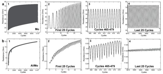
Figure 12.
A closer examination of representative in situ resistance data for the (a) Mo system and the (b) Al/Mo system. For both film systems, the full resistance data (1), the initial 25 cycles (2), the cycles ranging between 465 and 479 (3), and the last 25 cycles (4) are shown. Key features are the amplitudes of the resistance curves, the increasing average resistance, and the shape of the sine curves. Note the different y-axes for all parts.
A different electro-mechanical behavior was found for the Al/Mo system (Figure 12(b1)). For this film system, one of the intermittent samples, namely the bottom left sample of Figure 9 (R0 = 3.4 Ohm), was further analyzed. The full resistance as a function of cycles has a similar maximum resistance evolution to the Mo film, but at a much lower resistance. There is no large amplitude of the resistance during the first 25 cycles (Figure 12(b2)); rather, the maximum resistance continuously increases with the resistance amplitude remaining small. In the first 25 cycles, the resistance curves do have a plateau shape (flat top). Such a shape was shown by Gebhart et al. [28] to be an indication of TTC formation in Au and Au/Cr films. With more cycles (Figure 12(b3)), the resolution of the resistance is not good enough to track a possible plateau, but the amplitude is much smaller, less than 1 Ω (see y-axes), and the average resistance continues to increase. The continuously increasing resistance most likely indicates that more damage is forming, probably at a slower rate. By the end of the experiment shown in Figure 12(b4), the resistance amplitude is even smaller and there is an increase in the average resistance, but again, at an even slower rate. Thus, damage continues to form, but there are still pathways for conductivity (Figure 11).
The TTC formation can be detected in R/R0 in the following way. During bending, the resistance must increase because the sample is elongated (globally) and TTCs are extended. Near the maximum applied bending strain, the resistance reaches a plateau, indicating that the collective crack lengths have reached a saturation length for that cycle. As the sample straightens out, the resistance decreases due to local crack closure and global shortening of the sample. Then, the cycle is repeated until cracks can no longer extend, due to crack shielding effects. One needs to remember that each sine curve is the collective electrical resistance of the whole sample and not the resistance of only one crack in the sample.
4.3. Standardization
The comparison of the two different, but highly similar, 90° bending tests demonstrates that real disparities in the mechanical damage and electrical response after 10,000 bending cycles of the same material system were found. The main sources of difference, already addressed, are the rate of bending or folding and if the sample experiences spring back. If similar variances are found in the comparison of other bending tests, then there is no way to properly compare the results from different bending test geometries (Figure 2).
What is important to note from this study is that with the 90° bending, there is only one area of damage, and damage in this area can be fully quantified both in terms of the mechanical damage and the electrical resistance. Other methods (Figure 2) have multiple areas of damage. As it has been shown in this study, it is imperative to know where and when cracks are forming in order to properly understand the measured resistance, be it ex situ or in situ.
Compared to shear bending methods, with their area of damage that changes size, having only one well-defined area of damage simplifies the correlation between mechanical damage evolution and the electrical resistance. Furthermore, a standard sample geometry and preparation method (pre-cut vs. post-cut substrates) should also be adopted. Here, pre-cut samples were chosen to avoid inducing cracks from cutting the samples after deposition. Samples that were 9 mm wide were also chosen specifically so that cracks have a long way to travel before the resistance reaches overflow and to have a large area under the grips for measuring the electrical resistance. The measured resistance values do not contain additional undamaged areas when intermittent electrical measurements are utilized (outside the area directly under the grips). As demonstrated by Kreiml et al. [27], the electrical response and mechanical damage can be somewhat correlated when only the damaged area is considered. Also important is the speed of the test. Faster tests induced more damage than slower tests.
With the new knowledge from this study, a standard experimental protocol for all bending test geometries can be established to correlate the electrical response with the mechanical damage. Such a standard protocol would allow for results from the different geometries to be compared at least in a qualitative way. Four aspects are necessary to improve testing for foldable or rollable systems. One should know where the damage forms so that (1) the damage can be quantified similar to fragmentation testing (tensile testing). The electrical resistance should be evaluated in situ or ex situ of the damaged area (2a). If there are in situ electrical resistance data, they should be further analyzed in some way; at the least, the maximum and minimum values related to the opening and closing of cracks should be appraised and reported (2b). (3) A comparison of the mechanical damage and electrical resistance as a function of strain or cycles should be made and the average damage density or spacing (1/λ or λ) of the most affected area should be reported. Finally, (4) the appropriate and meaningful failure criteria can be applied that consider the electrical degradation and take mechanical damage evolution into account.
5. Conclusions
Two 90° bending tests, namely the custom-built FLEX-E-TEST and the commercially available YUASA test, were compared using the same samples, testing protocol, and characterization methods to determine if differences were observed. From the intermittent experiments up to 10,000 cycles, it was revealed that similar damage densities for both setups were achieved. However, the R/R0 were always higher for the samples tested on the FLEX-E-TEST. The main difference between the two setups is the speed of bending (YUASA strain rate is 16 times lower) and spring back of the sample (FLEX-E-TEST). A close examination of the mechanical damage with SEM micrographs exposed short TTCs formed on samples tested on the slower YUASA, while long TTCs formed on samples tested on the FLEX-E-TEST. In situ resistance data from the YUASA setup hint that TTC formation and propagation occur almost immediately as the shape of the R/R0 sine curves exhibited plateaus. These plateaus have been linked to TTC growth on other bilayer film systems. Through a more in-depth consideration of the in situ resistance data, it can be concluded that the resistance is influenced by both the density of TTCs and the effective crack lengths. The combined experiments aid towards understanding how flexible thin film systems fail both mechanically and electrically under bending and a new workflow for fully characterizing the electro-mechanical behavior has been presented. The new workflow should help researchers in the field to better compare results from different groups or different bending geometries. Therefore, it is probably more useful to have a set electrical failure criterion, such as the 20%–25% increase in resistance ratio, to determine when a film system is considered failed. For the two film systems investigated, the Mo/PI failed almost immediately, and the Al/Mo/PI to only 100 cycles on the FLEX-E-TEST and up to 1000 cycles on the YUASA.
Author Contributions
Conceptualization, M.J.C., H.K. and C.M.; methodology, P.K. and M.J.C.; formal analysis, P.K. and M.J.C.; investigation, P.K.; writing—original draft preparation, P.K. and M.J.C.; writing—review and editing, M.J.C., P.K., C.M. and H.K.; visualization, M.J.C. and P.K.; supervision, M.J.C. and C.M.; funding acquisition, C.M., H.K. and M.J.C. All authors have read and agreed to the published version of the manuscript.
Funding
This work was supported by the Austrian Research Promotion Agency (FFG) under Grant 857043.
Data Availability Statement
All data will be provided upon reasonable request.
Acknowledgments
The authors thank H. Sandner and K. Ruderes from the Erich Schmid Institute of Materials Science of the Austrian Academy of Sciences for experimental support and K.H. Pichler from the Department of Materials Science of the Montanuniversität Leoben for support during deposition. Plansee SE is gratefully acknowledged for the use of the YUASA device to perform this study.
Conflicts of Interest
The authors declare no conflicts of interest. The funders had no role in the design of the study; in the collection, analyses, or interpretation of data; in the writing of the manuscript; or in the decision to publish the results.
References
- Saleh, R.; Barth, M.; Eberhardt, W.; Zimmermann, A. Bending Setups for Reliability Investigation of Flexible Electronics. Micromachines 2021, 12, 78. [Google Scholar] [CrossRef] [PubMed]
- Glushko, O.; Cordill, M.J.; Klug, A.; List-Kratochvil, E.J.W. The Effect of Bending Loading Conditions on the Reliability of Inkjet Printed and Evaporated Silver Metallization on Polymer Substrates. Microelectron. Reliab. 2016, 56, 109–113. [Google Scholar] [CrossRef]
- Kim, B.J.; Shin, H.A.S.; Lee, J.H.; Yan, T.Y.; Haas, T.; Gruber, P.; Chou, I.S.; Kraft, O.; Joo, Y.C. Effect of Film Thickness on the Stretchability and Fatigue Resistance of Cu Films on Polymer Substrates. J. Mater. Res. 2014, 29, 2827–2834. [Google Scholar] [CrossRef]
- Ma, Q. A Four-Point Bending Technique for Studying Subcritical Crack Growth in Thin Films and at Interfaces. J. Mater. Res. 1997, 12, 840–845. [Google Scholar] [CrossRef]
- Yang, M.; Chon, M.W.; Kim, J.H.; Lee, S.H.; Jo, J.; Yeo, J.; Ko, S.H.; Choa, S.H. Mechanical and Environmental Durability of Roll-to-Roll Printed Silver Nanoparticle Film Using a Rapid Laser Annealing Process for Flexible Electronics. Microelectron. Reliab. 2014, 54, 2871–2880. [Google Scholar] [CrossRef]
- Park, S., II; Ahn, J.H.; Feng, X.; Wang, S.; Huang, Y.; Rogers, J.A. Theoretical and Experimental Studies of Bending of Inorganic Electronic Materials on Plastic Substrates. Adv. Funct. Mater. 2008, 18, 2673–2684. [Google Scholar] [CrossRef]
- Alzoubi, K.; Lu, S.; Sammakia, B.; Poliks, M. Experimental and Analytical Studies on the High Cycle Fatigue of Thin Film Metal on PET Substrate for Flexible Electronics Applications. IEEE Trans. Compon. Packag. Manuf. Technol. 2011, 1, 43–51. [Google Scholar] [CrossRef]
- Van Den Ende, D.A.; Van De Wiel, H.J.; Kusters, R.H.L.; Sridhar, A.; Schram, J.F.M.; Cauwe, M.; Van Den Brand, J. Mechanical and Electrical Properties of Ultra-Thin Chips and Flexible Electronics Assemblies during Bending. Microelectron. Reliab. 2014, 54, 2860–2870. [Google Scholar] [CrossRef]
- Bensaid, B.; Boddaert, X.; Benaben, P.; Gwoziecki, R.; Coppard, R. Reliability of OTFTs on Flexible Substrate: Mechanical Stress Effect. Eur. Phys. J. Appl. Phys. 2011, 55, 23907. [Google Scholar] [CrossRef]
- Trinks, C.; Volkert, C.A. Transition from Dislocation Glide to Creep Controlled Damage in Fatigued Thin Cu Films. J. Appl. Phys. 2013, 114, 093510. [Google Scholar] [CrossRef]
- Abdallah, A.A.; Bouten, P.C.P.; de With, G. Experimental Study on Buckle Evolution of Thin Inorganic Layers on a Polymer Substrate. Eng. Fract. Mech. 2010, 77, 2896–2905. [Google Scholar] [CrossRef]
- Lee, H.-Y.; Yi, S.-M.; Lee, J.-H.; Lee, H.-S.; Hyun, S.; Joo, Y.-C. Effects of Bending Fatigue on the Electrical Resistance in Metallic Films on Flexible Substrates. Met. Mater. Int. 2010, 16, 947–951. [Google Scholar] [CrossRef]
- Mao, L.; Meng, Q.; Ahmad, A.; Wei, Z. Mechanical Analyses and Structural Design Requirements for Flexible Energy Storage Devices. Adv. Energy Mater. 2017, 7, 1700535. [Google Scholar] [CrossRef]
- Agrawal, D.C.; Raj, R. Measurement of the Ultimate Shear Strength of a Metal-Ceramic Interface. Acta Metall. 1989, 37, 1265–1270. [Google Scholar] [CrossRef]
- Kreiml, P.; Rausch, M.; Terziyska, V.L.; Winkler, J.; Mitterer, C.; Cordill, M.J. Compressive and Tensile Bending of Sputter Deposited Al/Mo Bilayers. Scr. Mater. 2019, 162, 367–371. [Google Scholar] [CrossRef]
- Schwaiger, R.; Kraft, O. Size Effects in the Fatigue Behavior of Thin Ag Films. Acta Mater. 2003, 51, 195–206. [Google Scholar] [CrossRef]
- Hassan, T.; Liu, Z. On the Difference of Fatigue Strengths from Rotating Bending, Four-Point Bending, and Cantilever Bending Tests. Int. J. Press. Vessel. Pip. 2001, 78, 19–30. [Google Scholar] [CrossRef]
- Guan, Q.; Laven, J.; Bouten, P.C.P.; de With, G. Mechanical Failure of Brittle Thin Films on Polymers during Bending by Two-Point Rotation. Thin Solid Films 2016, 611, 107–116. [Google Scholar] [CrossRef]
- Abdallah, A.A.; Kozodaev, D.; Bouten, P.C.P.; Den Toonder, J.M.J.; Schubert, U.S.; De With, G. Buckle Morphology of Compressed Inorganic Thin Layers on a Polymer Substrate. Thin Solid Films 2006, 503, 167–176. [Google Scholar] [CrossRef]
- Kamiya, S.; Izumi, H.; Sekine, T.; Shishido, N.; Sugiyama, H.; Haga, Y.; Minari, T.; Koganemaru, M.; Tokito, S. A Multidimensional Scheme of Characterization for Performance Deterioration Behavior of Flexible Devices under Bending Deformation. Thin Solid Films 2020, 694, 137613. [Google Scholar] [CrossRef]
- Yi, S.M.; Choi, I.S.; Kim, B.J.; Joo, Y.C. Reliability Issues and Solutions in Flexible Electronics Under Mechanical Fatigue. Electron. Mater. Lett. 2018, 14, 387–404. [Google Scholar] [CrossRef]
- Kim, B.-J.; Haas, T.; Friederich, A.; Lee, J.-H.; Nam, D.-H.; Binder, J.R.; Bauer, W.; Choi, I.-S.; Joo, Y.-C.; Gruber, P.A.; et al. Improving Mechanical Fatigue Resistance by Optimizing the Nanoporous Structure of Inkjet-Printed Ag Electrodes for Flexible Devices. Nanotechnology 2014, 25, 125706. [Google Scholar] [CrossRef]
- Wright, D.N.; Vardøy, A.S.B.; Belle, B.D.; Visser Taklo, M.M.; Hagel, O.; Xie, L.; Danestig, M.; Eriksson, T. Bending Machine for Testing Reliability of Flexible Electronics. In Proceedings of the 2017 IMAPS Nordic Conference on Microelectronics Packaging, NordPac 2017, Gothenburg, Sweden, 18–20 June 2017; Institute of Electrical and Electronics Engineers Inc.: New York, NY, USA, 2017; pp. 47–52. [Google Scholar]
- Glushko, O.; Kraker, P.; Cordill, M.J. Explicit Relationship between Electrical and Topological Degradation of Polymer-Supported Metal Films Subjected to Mechanical Loading. Appl. Phys. Lett. 2017, 110, 191904. [Google Scholar] [CrossRef]
- Cordill, M.J.; Kreiml, P.; Mitterer, C. Materials Engineering for Flexible Metallic Thin Film Applications. Materials 2022, 15, 926. [Google Scholar] [CrossRef] [PubMed]
- Lu, N.; Wang, X.; Suo, Z.; Vlassak, J. Metal Films on Polymer Substrates Stretched beyond 50%. Appl. Phys. Lett. 2007, 91, 2–4. [Google Scholar] [CrossRef]
- Kreiml, P.; Rausch, M.; Terziyska, V.L.; Köstenbauer, H.; Winkler, J.; Mitterer, C.; Cordill, M.J. Correlation of Mechanical Damage and Electrical Behavior of Al/Mo Bilayers Subjected to Bending. Thin Solid Films 2019, 687, 137480. [Google Scholar] [CrossRef]
- Gebhart, D.D.; Krapf, A.; Gammer, C.; Merle, B.; Cordill, M.J. Linking Through-Thickness Cracks in Metallic Thin Films to in-Situ Electrical Resistance Peak Broadening. Scr. Mater. 2022, 212, 114550. [Google Scholar] [CrossRef]
- Cordill, M.J.; Kreiml, P.; Putz, B.; Mitterer, C.; Thiaudière, D.; Mocuta, C.; Renault, P.-O.; Faurie, D. Role of Layer Order on the Equi-Biaxial Behavior of Al/Mo Bilayers. Scr. Mater. 2021, 194, 113656. [Google Scholar] [CrossRef]
- Rausch, M.; Sabag, A.; Pichler, K.-H.; Gruber, G.C.; Köstenbauer, J.; Köstenbauer, H.; Kreiml, P.; Cordill, M.J.; Winkler, J.; Mitterer, C. The Sputter Performance of an Industrial-Scale Planar Mo-Target over Its Lifetime: Target Erosion and Fi Lm Properties. Surf. Coat. Technol. 2020, 381, 125174. [Google Scholar] [CrossRef]
- Sim, G.D.; Hwangbo, Y.; Kim, H.H.; Lee, S.B.; Vlassak, J.J. Fatigue of Polymer-Supported Ag Thin Films. Scr. Mater. 2012, 66, 915–918. [Google Scholar] [CrossRef]
- Sim, G.-D.; Lee, Y.-S.; Lee, S.-B.; Vlassak, J.J. Effects of Stretching and Cycling on the Fatigue Behavior of Polymer-Supported Ag Thin Films. Mater. Sci. Eng. A 2013, 575, 86–93. [Google Scholar] [CrossRef]
- Kreiml, P.; Rausch, M.; Terziyska, V.L.; Köstenbauer, H.; Winkler, J.; Mitterer, C.; Cordill, M.J. Improved Electro-Mechanical Reliability of Flexible Systems with Alloyed Mo-Ta Adhesion Layers. Thin Solid Films 2021, 720, 138533. [Google Scholar] [CrossRef]
- Sim, G.D.; Won, S.; Jin, C.Y.; Park, I.; Lee, S.B.; Vlassak, J.J. Improving the Stretchability of As-Deposited Ag Coatings on Poly-Ethylene-Terephthalate Substrates through Use of an Acrylic Primer. J. Appl. Phys. 2011, 109, 073511. [Google Scholar] [CrossRef]
- Glushko, O.; Klug, A.; List-Kratochvil, E.J.W.; Cordill, M.J. Relationship between Mechanical Damage and Electrical Degradation in Polymer-Supported Metal Films Subjected to Cyclic Loading. Mater. Sci. Eng. A 2016, 662, 157–161. [Google Scholar] [CrossRef]


Disclaimer/Publisher’s Note: The statements, opinions and data contained in all publications are solely those of the individual author(s) and contributor(s) and not of MDPI and/or the editor(s). MDPI and/or the editor(s) disclaim responsibility for any injury to people or property resulting from any ideas, methods, instructions or products referred to in the content. |
© 2024 by the authors. Licensee MDPI, Basel, Switzerland. This article is an open access article distributed under the terms and conditions of the Creative Commons Attribution (CC BY) license (https://creativecommons.org/licenses/by/4.0/).