
A Review on Preparation of Palladium Oxide Films


National Institute of Materials Physics, Atomistilor 405A, 077125 Măgurele, Romania
*
Author to whom correspondence should be addressed.
Coatings 2024, 14(10), 1260; https://doi.org/10.3390/coatings14101260
Submission received: 30 June 2024
/
Revised: 20 September 2024
/
Accepted: 24 September 2024
/
Published: 1 October 2024
(This article belongs to the Special Issue Advances of Nanoparticles and Thin Films)
Abstract
:Fabrication aspects of PdO thin films and coatings are reviewed here. The work provides and organizes the up-to-date information on the methods to obtain the films. In recent years, the interest in Pd oxide for different applications has increased. Since Pd can be converted into PdO, it is instructive to pay attention to the preparation of the pure and the alloyed Pd films, heterostructures, and nanoparticles synthesized on different substrates. The development of PdO films is presented from the early reports on coatings’ formation by oxidation of Pd foils and wires to present technologies. Modern synthesis/growth routes are gathered into chemical and physical categories. Chemical methods include hydrothermal, electrochemical, electroless deposition, and coating methods, such as impregnation, precipitation, screen printing, ink jet printing, spin or dip coating, chemical vapor deposition (CVD), and atomic layer deposition (ALD), while the physical ones include sputtering and cathodic arc deposition, laser ablation, ion or electron beam-induced deposition, evaporation, and supersonic cluster beam deposition. Analysis of publications indicates that many as-deposited Pd or Pd-oxide films are granular, with a high variety of morphologies and properties targeting very different applications, and they are grown on different substrates. We note that a comparative assessment of the challenges and quality among different films for a specific application is generally missing and, in some cases, it is difficult to make a distinction between a film and a randomly oriented, powder-like (granular), thin compact material. Textured or epitaxial films of Pd or PdO are rare and, if orientation is observed, in most cases, it is obtained accidentally. Some practical details and challenges of Pd oxidation toward PdO and some specific issues concerning application of films are also presented.
1. General Considerations on the Growth of PdO Films and Early Research as the Background of the Present Study
1.1. General Considerations on the Growth of PdO Films
According to the International Union of Pure and Applied Chemistry (IUPAC) [1], “A film is defined as a generic term referring to condensed matter restricted in one dimension. The term thin film is associated to a film whose thickness is of the order of a characteristic scale (i.e., a parameter which characterizes the density profile of a given physical quantity, which can have a static—equilibrium—or dynamic character that should be specified, e.g., terms out of plane and in plane refer to characteristic lengths normal or parallel to film surface, respectively) or smaller. Since a film may ‘look’ operationally thin or thick, according to the procedure applied, it is recommended that the measurement procedure employed be specified (e.g., ellipsometrically thin film, optically thin film, or, e.g., thick compared to the electron mean free path, thin compared to the optical wavelength, etc.)”.
In this review on preparation techniques of palladium oxide films, the presentation will stick to understanding that films are 2D objects and they are obtained on a substrate, unless otherwise mentioned, as for the cases of free-standing films. Thickness below about 10–30 nm, i.e., containing up to ~100 Pd(II) oxide unit cells (tetragonal with lattice constants a = 0.3035 nm and c = 0.5323 nm [2]), is often associated in the literature with the term ‘ultrathin’ films. Typical thin films are usually of few hundreds of nm, while thick films exceed 1 µm in thickness.
It is emphasized that many of the palladium oxide films are granular (i.e., composed of individual, well-defined particles with simple or complex morphologies). Often, a clear delimitation between the methods and procedures to obtain particles in a powder (on a substrate) and in a thin film is not possible. In this work, mostly the technologies demonstrated to produce a conventional relatively continuous film, usually with macroscopic surfaces useful for device fabrication, are briefly introduced. These films are Pd(II) monoxide films, although palladium shows different oxidation states. The common ones are 0, +1, +2, and +4 [3]. The most important oxide forms are the monoxide PdO, dioxide PdO2, and trioxide PdO3, as well as a hydrated sesquioxide Pd2O3 × H2O [4]. In the organic synthesis methods, Pd(0) and Pd(II) are usually considered [5].
Oxidation states +3 and +6 have been reported [6,7,8] in intermediate compounds proposed to occur in the palladium-catalyzed cross-coupling reactions. Authors of [9] theoretically studied the stability and activity of Pd4Ox (x = 1–7) films on Pd metal within a CO oxidation reaction model. Other articles also present nonstoichiometric palladium oxides PdO1−x [4,10]. Finally, there are films in the literature referred to as Pd/PdO that assume a Pd core region covered by a Pd-oxide surface layer. These types of particles and thin films (including materials marked with PdO/Pd), containing both metal and oxide species, are of interest for various applications, especially where oxidation–reduction processes play an important role. Since there are no generally accepted terms, on many occasions, materials described as Pd or PdO are in fact a mixture of the metal and oxide [11].
1.2. Early Research as the Background of the Present Study
Three groups of methods for film preparation are available:
- (1)
- Preparation of a Pd metal coating on a substrate, followed by oxidation.
- (2)
- Preparation of a PdO film by thermal decomposition of salts.
- (3)
- Preparation of the PdO oxide films by reactive methods.
The proposed classification is arbitrary, and often technological routes share the same processing steps and raw materials. Considering this, in this presentation, this classification is not strictly followed.
An early approach was to use a Pd metal foil or wire as a substrate, subject to surface oxidation. The functional product would be a PdO film coated on the Pd metal. This configuration was used as a pH sensor at high temperatures in geothermal brines, corrosive liquids in contact with nuclear waste containers, pressurized steam/water lines in power generation, and pressurized chemical reactors [12]. These electrodes are also suitable for measurements of pH in biological environments, such as blood and extracellular fluids [13,14], or for neurophysiological measurements [15]. It is well known that PdO is biocompatible, hence, it can also be used in wearable devices.
A high-temperature pH electrode should provide a direct voltage response to a pH value, negligible ionic and redox interfaces, minimum hysteresis, and drift. Only the oxide should be in contact with the solution. These requirements are difficult to fulfill in terms of palladium oxide thin films’ quality and thickness. An additional needed condition is miniaturization and low cost [13,16].
Three methods were attempted for fabrication of the Pd oxide film on Pd metal foils or wires:
- (i)
- Betteridge and Rhys [17] demonstrated that, when the Pd metal is heated to 700 °C in air, a PdO film forms on its surface. The electrode was not stable, and the utility of the thermal oxidation method for these purposes was reconsidered.
- (ii)
- Grubb and King [14] used chemical oxidation of the metal surface. The Pd metal surface, after cleaning in aqua regia for 20 s and roughening, was dipped into a 50% aqueous solution of NaOH and dried for 10 min in a stream of dry nitrogen. The coated Pd wire was heated in a flow of oxygen at 800 °C for 20 min. The portion covered with NaOH resulted in formation of a black PdO layer. The oxide layer was uniform, nonporous, and its thickness was of about 6 µm. Kinoshita et al. [18] expanded this research and studied different parameters, such as oxidation temperature in the range of 600 and 870 °C. They found that the best results were obtained for the electrodes processed at 750 °C after having been immersed in a 50% NaOH solution.
Thermal oxidation and chemical oxidation, as presented in points (i) and (ii), need relatively high processing temperatures. This impedes the preparation of oxide films and devices on low-temperature substrates, such as flexible ones (plastics, paper, and textiles), although Pd films have been coated by other methods on flexible, elastomeric, or optical fiber substrates [19,20,21,22]. Another inconvenience is that the reproducibility and stability of the oxide electrodes produced by the two addressed routes have been found to be highly sensitive to processing conditions, electrodes’ design, and sizes. Other important issues are stoichiometry control of PdO vs. oxidation temperature and decomposition of PdO. Decomposition of PdO was established both theoretically and experimentally to occur above 870–900 °C [23]. Some practical aspects regarding oxidation are addressed in the next paragraphs, while details in terms of time and spatial development of the metal–oxide interface will not be approached in detail.
Considering the presented information, the search for new methods to obtain PdO films on Pd or on other substrates has continued.
- (iii)
- An alternative method was proposed, namely, the electrochemical oxidation. Kinoshita et al. [18] oxidized the metal electrodes by treating them in 0.2 M NaOH for 5 min at 2.7 V and for 17 h at 0.74 V. Electrodes lost their near-Nernstian response to pH after a few acid–base cycles. A longer lifetime of less than 6 days was determined for an electrode fabricated by Liu et al. [13]. The authors used a molten salt electrolyte of NaNO3/LiCl for oxidation, with a current density of 20 mA·mm−2 at 5.9–6.2 V for 90 s. In [24], the authors applied electrolysis waveforms containing various levels of the ac and dc components for a processing time up to 24 h. The pH sensor’s response depends on the processing conditions. The authors also observed surface morphology changes.
Recent review articles summarize the work on synthesis of powders and coatings of Pd [3,25,26,27]. Powders and granular films of Pd or Pd-based materials are intensively investigated and used as catalysts. Rare are cases when they are oxidized to obtain palladium oxide as a product, although the methods from points (i)–(iii) are expected to also be successful in these cases. A straightforward example is thermal oxidation (in air at 300 °C for 2h) of PdCo nanoparticles and formation of a PdO-doped Co2O3 nano-powder [28,29].
Oxidation can be a general route to obtain Pd-based oxide, oxide compounds, or oxide composites from a large class of Pd-based alloys. Although, as already pointed out, oxidation of many reported Pd products was not performed, in the next paragraphs in this section, some details regarding the types of alloys and the methods used for their synthesis are introduced. Whenever available, the information on oxidation is also provided.
Palladium is shown to combine with other metals. Bimetallic or ternary alloys in the nano-powder form were synthesized: Pd-Pt, Pd-Au, Pd-Ag, Pd-Co, Pd-Co-Au, Pd-Cu, Pd-Ni, Pd-Rh, PdBi, Pt-Pd-Bi ([25,27] and references therein, [11,30,31,32,33]), Pd-Fe [34], and Pd-Ti [3]. Heterostructures and supported catalysts can enhance the chemical performance due to cooperative and synergetic interactions of the components [35]. In these cases, one takes advantage at the interface between Pd and the support on the charge transfer, strain effects, nanoscale surface stabilization, preferential faceting, prevention of the catalyst deactivation and regeneration, control of selective catalytic oxidation reactions, and improved gas-poisoning resistance. Supports of Pd tested in the literature are carbon black, activated carbon, carbon spheres, carbon nanofibers, single-wall (SWCNT) and multiwall (MWCNT) carbon nanotubes, graphene (G) and graphene oxide (GO), nanodiamond [36,37,38,39,40,41,42,43,44,45], Ti, TiO2, TiO2 nanotubes, Fe2O3, MnO2, V2O3, ZnO ([25] and references therein, [46]), Fe3O4, Fe3O3-C core-shell microsphere, Fe3O4-polyaniline and Fe3O4-NiSiO3 composites ([47] and references therein), CeO2 [48,49], CuO [26,50], sulfur-doped WO3 [51,52], Cr2O3 [53], MgO [54], La2O3 [55], kaolin [56], CuMn2O4 [57], MnSiOx [58], FeCrAl fibers [59], NiO [60], Co oxide [61], In-Sn-Zn-O-sputtered thin films [62], and wool [63]. Catalysts of Pd nanoparticles in which GO particles are encapsulated are also reported [64]. We observed that many of the supports are oxides stable at oxidation temperatures of metallic Pd and, therefore, they can be useful, depending on applications, as substrates for thin-film preparation of PdO-based materials. Other supports for Pd metal or alloy clusters are micelles, dendrimers, and mesoporous materials (e.g., polycarbonate, carbon tube, alumina, porous Ni, SiO2, and zeolite) [65,66]. Often, these supporting materials play the role of hard nanostructured templates, and the skeleton of the synthesized Pd objects follows the porous architecture of the support [3]. Materials of Pd/PdO clusters in glasses were also fabricated [67]. Apart from the use of templates, the crystal chemistry of Pd as a cubic face-centered (fcc) metal is itself highly favorable to formation of different geometrical shapes/morphologies [68] of the particles, both in the powders and in the coatings. The resulting morphology is controlled through manipulation of the thermodynamic aspects, involving high reduction rates, or of the anisotropy kinetics of the crystal growth. Size and especially morphology have a strong impact on the catalytic properties of nanocrystals. Fabrication and catalytic activity of Pd or Pd-based powders composed of particles with well-defined morphology, uniformity, and size is currently a field of significant interest both from academia and industry. This is a rich domain that is developing fast and in which many excellent articles were published in recent years. Despite this tremendous effort, as already mentioned, research and development rarely proceed toward synthesis of Pd oxide products from the as-fabricated Pd or Pd alloys.
Instead of alloys, other precursors or raw materials can be used, and the technological routes usually employ two processing steps. In the first one, a precursor film is obtained and, in the second one, the precursor is decomposed, reacted, or oxidized to obtain the Pd oxide. An example of a modern route is the growth of a nanoparticulate PdO thin film by the Langmuir–Blodgett (LB) technique, followed by thermal decomposition of the multilayer precursor film of octadecylamine (ODA)–chloropalladate complex [69]. Many other modern synthetic routes usually have several processing steps, one of which is mandatory of a chemical type: a granular metallic Pd(0), alloy, or organometallic film/coating is obtained in the first step, and it is further used as a precursor for preparation of the Pd oxide film final product by decomposition/reaction/oxidation. Nevertheless, the final oxide film can also be prepared by physical methods and by one-step routes, reactive or not. In the next sections, the review will consider two groups of technologies, namely, chemical and physical. This classification is not strict and should be taken as arbitrary.
Depending on the application, it is of interest to also take into account the reduction of PdO into Pd. In [70], Pd nanoparticles were decorated on PdO hollow-shell supports through a one-step treatment with NaBH4. In this process, PdO is partially reduced to Pd. The H2 gas detection limit of this material is lower than 1 ppm, and the proposed strategy can be employed to extend the lifetime of the H2 gas sensors. Another approach is precipitation on the support particles. In [71], PdCl2 was precipitated on ZnO nanoparticles and decomposed at 500 °C to Pd. Decoration of different support particles (WO3, ZnO-Eu, ZnO, β-Bi2O3, In2O3, SnO2, and V2O5) with functional Pd [71,72,73,74,75,76,77,78,79,80,81,82,83,84,85,86,87,88,89] or PdO [88,90,91,92,93,94,95], mainly for improved gas-sensing applications, is gaining much attention.
2. Chemical Routes of PdO and Pd Precursor Films’ Growth
In the category of chemical preparation methods of PdO or Pd precursor films (Figure 1), hydrothermal, electrochemical, electroless deposition, and coating methods can be included, such as the already mentioned Langmuir–Blodgett method, impregnation, precipitation, screen printing, ink jet printing, spin or dip coating, chemical vapor deposition (CVD), including its popular variant atomic layer deposition (ALD), and green biosynthesis. Chemical routes may involve in situ oxidation or reduction processes (e.g., in reactive synthesis routes or salts’ decomposition routes). As mentioned in Section 1.2, additional processing steps for reduction or oxidation (such as thermal, chemical, and electrochemical treatments) are sometimes applied on the precursor films already deposited by physical or chemical routes.
2.1. Hydrothermal Method
The hydrothermal method was employed in [96] to obtain PdCd nanostructures on a Ti plate. The Ti substrate was introduced in the Teflon autoclave containing 10 mL of 5 mM PdCl2, 5 mM Cd(NO3)2·4H2O, and 1 M ammonium formate as a reducing agent. The Pd/Cd ratio was varied by the amount of Cd(NO3)2·4H2O precursor. The processing temperature was 180 °C for 2 h. The coated Ti plates were further heated in a furnace with a controlled Ar-flow atmosphere at 250 °C for 2 h. The PdCd film had a dendritic microstructure.
In other examples ([25] and references therein) of hydrothermal synthesis of Pd or Pd-based bimetallic nanomaterials, a popular source of Pd is H2PdCl4, and formaldehyde (CH2O) and ethylene glycol (EG) are used as reducing agents. Composite PdO/CoNi2S4 particles were obtained via the hydrothermal method in [97].
The hydrothermal method is considered a single-step green technology that can use nontoxic solvents, and it minimizes waste. On the other hand, the productivity of this method is relatively low, and synthesis of large amounts of nano-powders or of large film surfaces is challenging. Via hydrothermal synthesis, different controlled shapes, such as nanospheres, nano-cubes, nano-tetrapods, nanoporous bulks, nanowires/dendrites, and core-shell particles on different substrates, are obtained [25].
A facile sol-gel hydrothermal method to obtain PdO particles is presented in [98]. After dissolving PdCl2 in C2H5OH (0.1 Molar solution), 1 vol.% HCl is added to enhance the solubility of PdCl2. Stirring for 30 min results in a transparent brown solution. The solution is aged for 24 h, loaded into a Teflon hydrothermal capsule, and heated at 200 °C. The as-obtained brown powder is washed with D.I. water and annealed at 600 °C. The final powder is fine and black and is used in the electrophoretic deposition to obtain a PdO film covered with ITO on a glass substrate for H2 gas detection at room temperature (Figure 2).
Wang et al. [99], via the hydrothermal method at 200 °C, obtained a ring-like PdO-NiO architecture, with a lamellar structure of 3.5 μm in diameter composed of nanosheets with a thickness of ~15 nm, for CO gas detection, showing a relatively low operating temperature (180 °C) and a rapid response/recovery (2–3 s when exposed to 50 ppm CO).
2.2. Electrochemical Deposition
In the group of electrochemical deposition methods, in an electrochemical cell with two or three electrodes (working electrode, counter electrode, and reference electrode), the electrolyte is conductive, and it is also the source of Pd. A current or potential is applied on the electrochemical cell, and ions of Pd(+II) in solution will deposit in the metal state (Pd(0)) at the surface of electrodes. Depending on the current or potential features, different versions of electrochemical depositions were defined: cyclic voltammetry (CV), square-wave voltammetry (SWV), chronoamperometry (CA), chronopotentiometry (CP), chrono-coulometry (CC), and pulsed electrodeposition ([25] and references therein).
The electrochemical deposition is considered a simple, affordable, and relatively fast method. Popular Pd raw materials are PdCl2 and H2PdCl4, but other materials can be used, e.g., K2PdCl6 [100] or Pd(NH3)4Cl2 [101]. Different morphologies are obtained in the electrochemical deposition. Nanoparticles with diameters of 5–10 nm and nanorods or nanowires are the most common. Pd nano-horns or nanoparticles of PdAu tube-shaped heterostructures were electrochemically deposited in [100,102], while an AgPd coating (on an oxidized/activated stainless-steel substrate), tested as a beneficial catalyst for low-temperature fuel cells’ application, was obtained in [103]. Fabrication of nanostructured bimetallic Pd-Fe thin films and their electrodechlorination activity are reported in [104]. The electrochemical deposition allows the use of template substrates, e.g., anodized aluminum oxide (AAO) or porous anodic alumina (PAA) [25]. After the directional template-assisted growth into the parallel pores, the substrate is removed, and the product is a sort of film consisting of an array of Pd nanowires [101]. By using an AAO template and subsequent etching of PdCu nanorods, Pd nano-springs were obtained in [102]. An open-pore Pd foam was electrodeposited, and a Pd-CeO2 catalyst for environment processes was reported in [105]. It was observed that most works report deposition of metal particles and films, rather than of the Pd oxide. Additional information can be found in [25].
In [98], films of PdO nanoparticles were deposited on ITO-coated glass substrates (5 mm × 10 mm) with electrophoretic deposition (EPD). The anode is the ITO substrate, and the cathode is a Pt rod. The distance between electrodes was set to 1 cm, and the electrodes were placed in a 20 mL glass vessel. A PdO powder (0.1 g) obtained by the sol-gel hydrothermal method (see the previous paragraph) was dispersed in 10 mL of ethanol. In this electrolyte solution, as a dispersant and to enhance conductivity and mobility of the ions, magnesium nitrate (Mg(NO3)2·6H2O, 100 μL) was added. The deposition potential applied for 2 min was between 10 and 35 V. The authors indicated that the quality of the film depends on the deposition voltage and time. The optimum voltage would be 30 V. Films were used for H2 gas detection at room temperature by using an amperometric gas-sensing setup (Figure 2).
It is important to emphasize that PdO oxide films can be used not only for reduction gases’ detection, but also for oxidizing ones. An example of the results obtained with a chemoresistive (conductomeric) sensor sensitive to ozone is presented in Figure 3 [106].
The somehow related method of electrospinning is also a straightforward fabrication coating technique, and it was applied in [107] to obtain a decorated Pd nanolayer upon aligned polyurethane nanofibers for H2 gas sensors. Among the coatings obtained by electrospinning of PdO, Au, and CdO on SnO2 nanofibers, the highest sensitivity to toluene was determined for PdO-SnO2 [108].
2.3. Electroless Deposition
The group of electroless deposition techniques has two main variants, namely, the displacement (galvanic replacement) and autocatalytic deposition [25]. These methods take advantage of a photo-reductant, a stabilizer, or a chemical reducing agent. Microemulsion and photochemical synthesis also belong to these types of methods, which are without an external current source but share a common ground with electrochemical routes.
In the displacement deposition, 25 µL of 10 mM H2PdCl2 was placed on Fe thin films for 30 min [104]. Reactions between PdCl42−/Pd and Fe2+/Fe developed with standard redox potentials of 0.95 and −0.44 V, respectively. The final product was washed with ultrapure water and dried. The less noble metal acted as a reducing agent, and the reaction proceeded at its surface. This produced certain limitations. Other limitations were imposed by the required favorable difference in the reduction potentials of the two metals.
The autocatalytic deposition uses citric acid, ascorbic acid, ethylene glycol, sodium borohydride, and others as reducing agents. The impact of the reducing agent is very strong and can modify growth kinetics with changes in the particles’ morphology and in the surface properties ([25] and references therein). In general, the reducing agents are added into aqueous solutions of PdCl2, NaPdCl4, or H2PdCl4. The method is suitable to obtain bimetallic Pd-based nanomaterials. It also has the advantage that the processes proceed at the surface and in the bulk of the metals. The polyol synthesis is a derivate method. Metal-containing compounds are obtained through the use of ethylene glycol, playing the role of both the solvent and the reducing agent. Without templates, Wang et al. [109,110] synthesized nanowires with uniform diameters of 2 nm via this technique. Synthesis proceeded from a solution of (CF3COO)2Pd dissolved in diethylene glycol (DEG). When instead of (CF3COO)2Pd, the authors used Na2PdCl4, Pd polyhedrons were obtained.
Microemulsion techniques use water in oil to control the particle size. Surfactant-stabilized reverse micelles are the microreactors. Typical surfactants are dioctyl sodium sulfosuccinate (AOT) and cetyl trimethyl ammonium bromide (CTAB). In some cases, heptane is used as an oil phase, while toluene is a co-surfactant. Application of surface-confining agents, such as CO that are preferentially binding on the Pd(111) surface, produced nanosheets of Pd with a thickness of 1.8 nm [111]. Microemulsion is shown to be suitable for the synthesis of Pd-Co-Au/C tri-metallic catalysts [112]. Yuasa et al. [113] investigated preparation of composite particles of nano-sized PdO loaded on SnO2 nanoparticles by precipitating Pd(OH)2 and Sn(OH)4 inside a reverse micelle. CO gas-sensing properties of the particles were highly sensitive and were maximized for a small amount of PdO (0.1 mol %), at which PdO agglomeration is avoided. This method allows loading of small amounts of PdO when compared to the conventional impregnation method.
Nanoparticles of PdAu were obtained on TiO2 via photochemical synthesis. Tian et. al. [114] immersed a plate with TiO2 nanotubes into a water solution of 0.04 M Pd(NO3)2 and AuCl3. In the solution, 5 mL (50 vol.%) of methanol was also introduced. After 30 min of exposure to UV radiation, in the solution, PdAu particles with the size of ~20 nm formed.
2.4. Coating Techniques
The group of coating techniques, such as Langmuir–Blodgett, impregnation, precipitation, screen printing, ink jet printing, and dip and spin coating, due to their simplicity and low cost, are often employed to obtain Pd-based precursor powders or films [10,94,115,116,117,118]. The idea of these synthesis methods is to synthesize particles or films, usually of palladium chloride, nitrate, or hydroxide, which are subsequently thermally decomposed.
Jin et al. [119] used the conventional impregnation method by dipping a honeycomb cordierite substrate coated with CexZry oxides (synthesized by co-precipitation with urea of a Ce, Zr nitrate solution, and calcination at 550 °C in air) into the aqueous solution of palladium nitrate, followed by drying and calcination in air at 500 °C for 2 h, to obtain a brown-colored catalyst complex with Pd (metal loading on the monolith of about 0.3 wt.%). This material was investigated as an alternative catalytic technology to oxygen removal of coal mine methane. To optimize CO2 methanation pathways, coatings of Pd/P-CeO2-Al2O3 were prepared via multistep impregnation in [120].
In [121], decorated flower-like ZnO structures with PdO obtained by precipitation in a methanol solution with dispersed ZnO particles and with dissolved PdCl2 (60 mg ZnO, 3.3 mL methanol, and 6 mg PdCl2, shaken for 30 min), followed by calcination at 350 °C for 1 h (heating rate of 5 °C/min), showed better sensing activity of toluene and ethanol than of ZnO (Figure 4).
Use of PdCl2 as an initial reagent is economically convenient since it is produced at an industrial scale and it is relatively cheap, but traces of residual chloride anions can show a strong negative influence on the sensitivity of PdO gas sensors. For this type of device, it is recommended to convert PdCl2 (e.g., through a reaction with NaOH or AgNO3 [10]) or to use the palladium hydroxide or nitrate directly as initial reagents. The typical media to dissolve the initial reagents is water. Balamurugan et al. [118] dissolved Pd(NO3)2·H2O in weak triprotic citric acid monohydrate (C6H8O7·H2O). Powders or films are thermally decomposed in air or in dry oxygen to obtain PdO. In [10], PdO was obtained by decomposition of Pd nitrate at 400 and 600 °C in dry oxygen. In [115], samples of PdNO3 impregnated on La0.6Sr0.4Co0.2Fe0.8O3−x for cathodes in solid oxide fuel cells working at intermediate temperatures were calcinated at 800 °C for 2 h, in air. Nanohybrids of PdO-WO3 were obtained by annealing at 400 °C for 24 h in air to decompose PdCl2 into PdO on WO3 nanorods [117].
Other initial reagents than those already mentioned can be used. A proposed precursor material for spin coating is the β-ketoiminato palladium(II) complex [Pd(OAc)L] (L=PhC(O)CHC(Me)NCH2CH2NHCH2CH2NH(Me)C=CHC(O)Ph) [122]. It decomposes at 200–500 °C and forms Pd in argon and PdO in oxygen atmospheres. Kabcum et al. [117] impregnated 0.25–2.0 wt.% Pd onto WO3 powder using palladium acetylacetonate (Pd(C5H7O2)2 dissolved in ethanol. After drying at 80 °C for 24 h, a heat treatment was conducted at 300 °C for 2 h. The powder (60 mg) was mixed (30 min) with a homogeneous binder solution (0.28 mL) of ethyl cellulose dissolved (at 80 °C for 12 h) in α-terpineol solvent to obtain a paste. The paste was spin-coated at 3000 rpm for 30 s on Al2O3 substrates. Annealing was performed at 150 °C for 1 h and then at 450 °C for 2 h (heating rate of 1 °C/min) for binder removal. The advantage of using organometallic reagents as a precursor is that it is convenient for decreasing the decomposition temperature.
Thick films in the SnO2–CeO2–PdOx system were obtained by sol-gel screen printing on alumina substrates in [123]. A solution of 20 wt.% of SnCl4 in water was mixed with solutions of ceric ammonium nitrate and palladium chloride. Ammonium hydroxide solution (25% in water) was added dropwise to the mixture to obtain a pH of 9.0, followed by stirring for 20 min. The resulting solution was aged for one day at room temperature. The volatiles were removed under reduced pressure at 70 °C to obtain powders. Powders were used to obtain a paste that was screen-printed on ultrasonically cleaned alumina substrates with Au electrodes and with a heater on the backside. The printed films were heated at 700 °C for 2 h. The as-fabricated sensor had enhanced sensitivity for CO gas detection.
In [116], the precursor solution of a Pd-organoamine was spin-coated (500 rpm for 10 s, followed by 3000 rpm for 60 s, using an acceleration of 800 rpm/s in both stages) on glass substrates and annealed at 200 and 250 °C (4 min, 24 h, and 48 h). This approach allows ink jet printing, as demonstrated in [124]. Amine-stabilized Pd clusters were obtained after decomposition of the precursor. Subsequent thermolysis of the clusters under air yielded smooth films. Under nitrogen atmosphere, the films consisted of large micron aggregates, while in low vacuum, Pd/PdO bilayer films were obtained (Figure 5).
2.5. Chemical Vapor Deposition
A review on the growth via chemical vapor deposition (CVD) of iridium, platinum, rhodium, and palladium thin films is presented in [125]. The work indicated that for the deposition of Pd thin films, with the exception of PdCl2, the precursors were of organic type: metal β-diketonates (Pd(acac)2, Pd(hfac)2), allyl complexes (Pd(allyl)2, Pd(Me allyl)2, CpPd(allyl), Pd(allyl)(acac), Pd(allyl)(hfac), Pd(Me allyl)(hfac), Pd(Me allyl)(acac), alkyl complexes (PdMe2(PMe3)2, PdMe2(PEt3)2, and PdMe2(tmeda)), metal carboxylate (Pd(acetate)2), and ethylene complexes (Pd(C2H4)2), where acac = acetylacetonate = C5H7O2, hfac = hexafluoroacetylacetonate = C5HO2F6, allyl = η3-C3H5, Cp = cyclopentadienyl = η5-C5H5, tmeda = tetramethylethylenediamine = C6H12N2H2, acetate = C2H3O2, and vinyl = C2H4. Other organic precursors proposed and reported in recent years will be mentioned in the next paragraphs. The Pd thin films were also grown via CVD in [126,127,128,129]. The PdCu alloy films on Si or SiO2 substrates were deposited by CVD from a single-source precursor (β-diketonate complex) at 250–400 °C [129].
Among the CVD group techniques, the aerosol-assisted chemical vapor deposition (AACVD) is considered a promising variant, being simple and easy [130]. The precursor material was the commercially available palladium acetylacetonate, Pd(acac)2 (Pd(C5H7O2)2, 100 mg, 0.328 mM), dissolved in toluene (10 mL). The aerosol mist from Pd(acac)2 solution was generated by a piezoelectric ultrasonic humidifier. The aerosol was injected into the reactor tube with the help of a nitrogen (N2) gas flow (150 cm3/min). No hydrogen gas or any other reducing agents were used. Deposition for 30 min was performed on glass substrates heated to 475 °C.
Via AACVD, synthesis of palladium-nanoparticle-decorated WO3-nanoneedles was accomplished in a single step [131,132]. Two source materials were tested: palladium acetylacetonate and ammonium hexachloropalladate. The first one led to better quality: the response of the PdO-decorated WO3 toward hydrogen gas sensing was about 680–750 times higher than that of bare WO3 nanoneedles. The operation temperature was at relatively safe and low values of 50–150 °C, and the addition of PdO minimized the effect of humidity on the sensor’s response.
The AACVD was successfully demonstrated for fabrication of Pd-decorated WO3 H2 gas sensors on a flexible kapton substrate [133].
Pd nanoparticles were deposited by AACVD on an array of WO3 nanorods [134]. The source material was (NH4)2PdCl4 in a methanol solvent, the deposition temperature was 350 °C, and the N2 gas flow rate was 300 sccm. Oxidation to PdO was performed in air at 500 °C for 2 h.
In [135], films of Pd (20–120 nm) were prepared on glass substrates via plasma-enhanced metalorganic chemical vapor deposition (PEMOCVD). The source material was Pd(acac)2 (vapor pressure 0.1 hPa at 433 K) and the carrier gas was Ar (0.71 cm3 min−1). The total pressure in the deposition chamber was 4.5 Pa. The glow discharge power was 40 W. The sublimation temperature of Pd(acac)2 was found to influence the films’ composition relative to the Pd and C ratio in the as-deposited films. The optimum sublimation temperature was determined to be 413 K. Films were thermally decomposed at 623 K for 900 s, and they were composed of Pd nanoparticles in the range of 5–10 nm, which is considered suitable for catalytic activity.
In the CVD group methods, precursors are evaporated or sublimated and often show problems of thermal instability, resulting in poor quality and reproducibility of the as-deposited Pd film. To avoid formation of oxides is challenging, and the typically slow deposition rates in CVD are not convenient for high productivity and commercial fabrication. Some of the most popular gas-phase precursors are η3-allyl and β-diketonato palladium complexes [136,137,138]. Among those of the first type, [Pd(η3-C3H7)2] [139] and [Pd(η3-2-Me-C3H4)2] [140] show thermal instability during evaporation and storage. They are also highly sensitive to air and moisture [137]. Another problem is that without the aid of a reactive gas [140], the deposited Pd films contain a low amount of carbon impurity (1 wt.%). The precursors of the second type, bis (β-diketonato) palladium (II) complexes, such as [Pd(acac)2] (acac = acetylacetonate), are thermally stable, but their volatility is low, and they require higher decomposition temperatures [138]. A combination of the allyl and β-diketonate groups within one complex was proposed in [141] to overcome the deficiencies of each type. Other synthesized CVD precursors are β-ketoiminate [142], β-ketoiminato palladium (II) complexes, such as [Pd(CF3C(O)CHC(CF3)NnBu)2] [143,144], [Pd(CH3C(NH)CHC(O)CH3)2] [145,146], [Pd(CH3(O)CCHCN(CH3)(CH2)3)2)] [147], and [Pd(2-NC5H4)NHNCH-1-(O)-4-OMe-Ph)(PPh3)] [148], and palladium(II) allyl (β-ketoiminato) complexes [149], e.g., [Pd(ƞ3-2-Me-C3H4)(MeC(O)CHCMeNPh)]. The oxygen content in some of these precursors is minimized, leading to a lower oxidation of the substrate during formation of the metal film [145,146]. The complexes have a higher stability to air and moisture [150]. The search for new MOCVD source materials [151] continues, and it is one of the key priorities for the development of CVD technology.
Via atomic layer deposition (ALD), a variant of CVD, Pd thin films were successfully grown in [144,152,153,154,155,156,157]. In ALD, precursors are used that react with the surface of the substrate in a sequential way, one at a time. The chemisorbed metalorganic compound (e.g., β-ketoiminate [154] or Pd(II)(hfac)2 precursors [152]) decomposes under the influence of the second precursor, and the organic ligand is removed to form a metal film. The second precursor can be an organic (e.g., glyoxylic acid [152]) or a gas, such as oxygen [144]. In general, ALD is recognized as a technique that allows better control of the thickness and density. A recent review [157] on ALD of Pd pointed out the enhanced possibilities of this technique. Precise control of Pd deposited on challenging surfaces with different precursor chemistries and by using customizable processing conditions can generate low-dimensional nanostructures (single atoms, nanoclusters or nanoparticles, core-shell particles, and ultrathin films). The disadvantages of ALD are the slow deposition rate (in the range of nm/min) and that it allows growth of films with rather small surface areas.
2.6. Green Biosynthesis
The need for clean technologies led to a search of green biosynthesis routes ([5] and references therein). Natural, non-toxic, and eco-friendly precursor substances can be used to obtain usually metal particles. Examples of such substances are Aspalathus linearis (Rooibos) and Annona squamosa peel extracts, banana peel extract, Cinnamon zeylanicum bark, Curcuma longa tuber, broth of Cinnamon camphora leaf, Gum acacia, Solanum trilobatum leaf, Soybean leaf, Zanthan gum, or, more recently, Crocus sativus [158], coconut coir [159], Trigonella foenum-graecum (fenugreek) seed [159], Rosmarinus officinalis L. (rosemary) [160], and Zaleya decandra [161]. Among the most bioactive substances, aspalathin, nothofagin, and aspalalinin are considered. However, the choice of the plant and processing method and conditions are critical regarding the quality and quantity of the extracted compound. Aspalathus linearis leaves (0.03 g) were added to 300 mL of deionized water at room temperature for ~30 min [5]. The orange extract (pH~5) was filtered three times to remove solid residuals and was slightly fermented. In the as-prepared extract, PdCl2 (3 g) was added and fully dissolved under stirring at room temperature. After 30 min of reaction time necessary to complete the oxidation–reduction reaction, the color of the solution changed. By drying in air at 90 °C for 1 h, an amorphous product was obtained, which was further annealed for 2 h at 100 °C or at a higher temperature. The product annealed at 100 °C was composed of non-agglomerated crystalline nanoparticles with different morphologies and with an average mean size diameter of 12.7 nm. Via TEM, particles were ascribed to fcc cubic Pd. At higher annealing temperatures (200–600 °C), the product was oxidized. At intermediate temperatures, X-ray diffraction indicated co-existence of Pd and tetragonal PdO, while at 600 °C, only PdO was detected. Time and/or temperature to obtain PdO were considered [5,162] lower than for other processing routes, such as heating of PdCl2 in a NaNO3 melt, thermal decomposition of Pd(NO3)2·2H2O, oxidation of Pd in air or in oxygen, or direct carbon arc vaporization of Pd.
In [37], citric acid was used as a mild and environmentally friendly stabilizing and reducing agent to obtain nanohybrids of graphene oxide decorated with Pd. Graphene oxide was treated with aliphatic amines 1-octadecylamine and 1,8-diaminooctane, followed by addition of a palladium chloride in a liquid medium and citric acid.
3. Physical Routes of Pd and PdO Thin Films’ Growth
Through physical technological methods, either the Pd metal precursor or the Pd oxide films can be prepared in a single processing step. Among the physical methods are sputtering and cathodic arc deposition, laser ablation, ion or electron beam-induced deposition, evaporation, and supersonic cluster beam deposition (Figure 1).
3.1. Sputtering and Cathodic Arc Deposition
Sputtering a target of a metal through the bombardment with energetic ions of an inert gas (e.g., argon or helium) produces collision of these energetic ions with the target and ejects target metal atoms into space. These metal atoms are deposited on a substrate material, forming a metallic film. Sputtering is recognized as a fast-rate vacuum coating technique that allows creation of strongly adhesive coatings on substrates with complex geometries. Magnetron sputtering is popular for deposition of metals and oxides. The energetic ionic species and electrons are confined in a magnetically enhanced glow discharge. Confinement produces a relatively high plasma density and promotes acceleration of the ions, which will vaporize the source material (target). The ion or molecular ion-sputtered species from the target, i.e., Pd in this case, fly and deposit on the substrate. If oxygen, as a reactive gas, is introduced in the deposition chamber, one can obtain in situ Pd oxide films. In practice, to avoid oxygen contamination of the sputtering chamber, thermal oxidation of the as-prepared Pd films is preferred to direct reactive sputtering. Simultaneous co-sputtering from different targets is applied to obtain bi- or multi-component metal alloys. This is performed by tuning the power applied on each sputtering gun/target. The drawback of sputtering is considered its limitation in deposition of films into deep structures. The literature presents different solutions of directional sputtering approaches, such as collimated sputter deposition, elevated temperature/reflow deposition, long-throw sputter deposition, and ionized magnetron sputtering [163,164].
Thin films of PdO on (111) Si-wafers and alumina circuit-board substrates were deposited by magnetron sputtering from a Pd target in [12]. The deposition atmosphere was O2:Ar = 1:1 for a total pressure of 0.35 Pa (starting base pressure was (2–4) × 10−4 Pa). The as-grown film consisted of Pd oxide, according to XRD, but an unidentified impurity peak was detected at 2θ = 56°. The lattice parameters of PdO increased, and the XRD line of the impurity disappeared during post-annealing at 420 °C in air.
Yoon at et al. [165] deposited, for hydrogen gas sensors, Pd thin films (50 nm) by magnetron sputtering in Ar gas at a pressure of 1.2 × 10⁻² Torr (initial vacuum pressure was 1.2 × 10⁻⁶ Torr) and for an input power of 1000 W.
Via dc magnetron sputtering, Pd films were obtained in [166] on oxidized Si (SiO2 thickness was 100 nm) and for a source power of 60 W. The distance between the target and substrate was 10 cm, and an Ar atmosphere was used (initial vacuum was 10−6 Torr). When the deposition pressure was increased from 22 to 122 mTorr, the average grain size in the films changed from 10 to 30 nm.
Hao et al., via dc magnetron sputtering, obtained porous films of Pd on porous anodic aluminum oxide (AAO) templates for room-temperature chemoresistive hydrogen sensors [167] (Figure 6). After degassing the AAO substrate in a vacuum (1 × 10⁻³ Pa) by heating in the sputtering chamber at 100 °C, Pd films were deposited at ~50 °C in an Ar (99.999%) atmosphere (made from a vacuum of 4 × 10⁻⁴ Pa) at a pressure of 0.7 Pa. As-prepared Pd films (45 nm) were annealed for 30 min in the deposition chamber at 150, 200, 300, and 400 °C. It was shown that annealing decreased the response time (time delay to reach 90% of resistance), and the drift of the baseline for the annealed sensor was not observed.
Magnetron sputtering was also used in [168] to grow Pd thin films on Ti–6Al–7Nb plates. After a heat treatment in air at 450, 550, and 650 °C for 1 h, their mechanical, corrosive, and wettability properties and in vitro bioactivity were studied. These materials are considered for implant applications.
Other examples of PdO-sputtered films were reported in [169,170,171,172]. Reactive sputtering was employed to obtain PdO nanoflake thin films for CO gas sensing at low temperatures in [170,173]. Layers of Pd were incorporated by rf sputtering into an electrode-functional layer of a thin-film-based nickel–yttria-stabilized zirconia (Ni–YSZ) solid oxide cell (TF-SOC) [174]. Selective doping (Gd or Tb) of Pd films on (001) MgO for hydrogen gas sensing was performed by dc magnetron sputtering at 550 °C, and they showed the (002) preferred orientation [175]. PdO thin films [176] with nano-sized cracks (Figure 7), obtained in a vacuum atmosphere (base pressure of 4 × 10⁻⁸ Torr with 5, 10, 15, 20, 25, and 30% oxygen) by reactive sputtering at room temperature on oxidized (100) Si, demonstrated an ultrahigh sensitivity (~4.5 × 10³%) and a fast response time at room temperature to H2 gas in nitrogen.
A variant of sputtering, namely, the plasma-assisted sputtering, was performed in [177] for an ionization current of 3 mA under 1.0 × 10⁻¹ Torr. The thickness of the Pd nanostructures deposited on (001) GaN was in the range of 1–30 nm. Samples were annealed for 450 s at 650, 700, and 750 °C in a vacuum of 1.0 × 10⁻⁴ Torr, and evolution of the morphology was studied.
3.2. Electron Beam Coating and Electron and Ion Beam-Induced Deposition
For the growth of Pd films, electron and ion beam-induced deposition (EBID and IBID) were demonstrated. These methods were successful in fabrication of 3D structures/patterns [180]. In these vacuum-based techniques, a precursor material (usually of a metal-organic type) is introduced (injected) in the deposition chamber, and it is absorbed on a substrate. A focused electron or ion beam is used for processing the precursor and through its decomposition to obtain the film. Via IBID, and using Pd-bis(hexafluoroacetylaceacetonate) as the precursor film, a film composed of nanowires of Pd was obtained in [181]. EBID was applied in [182] on a spin-coated precursor film of Pd-hexadecathiolate on a Si substrate. These methods share similar features with two-step chemical methods that use a precursor Pd-based compound deposited in the first step and decomposed in the second one. A typical conventional electron beam coating to obtain a Pd film (with a thickness of 12.3 nm) was applied in [183]. The film was deposited on glass substrates. The base pressure before deposition was 3 × 10⁻⁵ mbar. The substrate temperature was 32 °C, cathode voltage was 8.5 kV, and coating rate was 12 A·s−1. Annealing was performed in air at 350, 450, 550, and 650 °C for 1 h. According to XRD, the films consisted of Pd phase. In [184], the electron beam gun was used to evaporate a Pd ingot target and deposit Pd thin films (17–100 nm) on a 2-inch Si wafer substrate with a sputtered buffer layer of SiO2 of 400 nm in thickness. The substrate was positioned at about 35 cm above the target. The film deposition was performed at 8 × 10⁻⁵ Pa in a vacuum chamber. XRD indicated that the Pd film was (111) oriented. The sheet resistance of the Pd film (50 nm) annealed at 100, 150, and 200 °C for 3 h was not affected up to 150 °C. In [185], Pd films were deposited by e-beam evaporation of palladium pellets (99.95%). The substrate was thick fused silica (1 mm) and, during deposition in the vacuum (base pressure of 10−4 Pa), it was heated at 90 °C. The growth rate of the film was set at 0.5 nm/s. The Pd films with thicknesses of 7.2 (S1), 12.6 (S2), 17.5 (S3), and 27.3 (S4) nm were oxidized by annealing at 500 °C in a vacuum at 150 Pa. The annealing time was selected to be 1 h for each 10 nm of the film’s thickness, ensuring the full oxidation of the films. The oxidized films were exposed for 10 min to H2 atmosphere (5 vol.% in nitrogen) at room temperature. This procedure reduced PdO to r-Pd, and the thickness of the samples decreased without restoring the initial one, while porosity increased (density decreased by 1.68–2.6 times). Films were used in room-temperature optical H2 gas sensors (Figure 8). A higher film thickness increased the response and recovery times of the as-prepared Pd films, and it was almost constant for r-Pd-treated films. Palladium films were deposited by electron beam evaporation on Si/SiO2/Pt substrates, and after annealing in oxygen at 500 °C for one hour to form the palladium oxide (PdO), films were tested for hydrogen ion (pH) sensing [186]. The authors found that the sensitivity of the device (extended-gate field-effect transistor (EGFET)) was 42.36 mV/pH.
3.3. Pulsed Laser Deposition
In the pulsed laser deposition (PLD), a pulsed laser is focused on a Pd or PdO [187,188,189,190,191] bulk target. Through ablation, the material from the target evaporates/sublimates or converts to a plasma, and it is directed on a substrate to form a film. Laser type (pulsed or continuous), wavelength, and its fluence, gas pressure in the deposition chamber, target–substrate distance, and substrate temperature are among the parameters to control the process and the film quality. Ablation of the Pd bulk targets can also be realized in a liquid instead of a gas environment, and the product is usually a nano-powder. The type of liquid was shown to influence not only the size and morphology, but also the oxidation and hydrogenation level of the resulting Pd particles [192]. Via this approach, ultra-small Pd nanoparticles were deposited on CdS nanorods for the photocatalytic hydrogen production [193]. The morphology and porosity of the bilayer films of Pd/TiO2 deposited by PLD (Nd-YAG laser, emission wavelength of 355 nm, 5 ns pulse duration, repetition rate of 10 Hz, energy per pulse of 71 mJ, energy density on the target of 25 J/cm2, target–substrate distance of 40 mm, and substrate temperature is room temperature) were modified by changing the oxygen and argon pressures. The films were deposited on the quartz substrate of surface acoustic wave (SAW) room-temperature H2 gas sensors [188]. The quality of Pd deposits versus the ablation process and Al2O3 substrate characteristics were reported in [187]. Pd was deposited by PLD on wood for Ni electroless plating in [194]. Different helium background gas pressures (50, 350, and 800 mTorr) during Pd thin films’ PLD deposition influence the crystallite size and the tendency of their orientation in the <111> direction [189]. Pd thin films of 0.4–4 monolayers were deposited on (001) Cu at room temperature by PLD. The Pd–Cu interface formation is characterized by an alloying–dealloying mechanism. Up to two monolayers, Pd atoms are incorporated into the Cu substrate for less than half-filled layers but expelled if the Pd coverage is close to a complete layer. In this latter case, the top layer is composed of Pd [195]. PLD was used for doping the surface of polycrystalline thin-film SnO2 or SnO2(Cu) gas sensors for the enhancement of the sensitivity to 1% H2 in N2 (at 200–380 °C), with two orders of magnitude [196]. Pd-doped SnO2 thin films for gas sensors were grown on (100) Si substrates using PLD at room temperature in [197]. The microstructure of the films depends on the O2 background pressure (10–100 Pa) and on the target–substrate distance. When the target–substrate distance was close to the plume length, textured thin films were obtained, and the authors explained this phenomenon considering an adiabatic expansion. Nanostructured Pd films obtained by PLD (KrF excimer laser, 248 nm, pulse time of 20 ns, repetition rate of 100 Hz, background pressure in the deposition chamber of 10−5 mbar, laser fluence of 5 ± 0.1 J/cm2 or 250 MW/cm2, the laser beam was focused at a 45° angle on the target with a spot area of 1 mm2, and Pd metal target with purity of 99.9%) have very different electrochemical characteristics from those of common coarse-grained films [198]. Stability was good under hydrogen charge/discharge cycling, and this was related to the lack of an abrupt α-to-β phase transition. Upon oxidation of Pd films with controlled thickness and grain size deposited by PLD, spontaneous formation of uniformly distributed arrays of conical PdO “tips” useful for field emission applications was reported in [191,199].
Chemoresistive acetone sensors of ZnO were decorated with Pd particles by PLD [200]. Sensors operated in the temperature range 159–200 °C, and they showed an enhancement of the response factor between 2 and 7 when compared with pure ZnO sensors. The detection limit was 26 ppm at 200 °C.
3.4. Evaporation (Sublimation) of Pd
Evaporation (sublimation) of Pd (e.g., a metal foil resistively heated by a V-shaped tungsten filament) and deposition is a simple and popular technique [106,201,202,203,204,205]. Evaporation was realized in a high-vacuum chamber (e.g., at 6.65 × 10⁻⁴ Pa in [84] or 18–57 × 104 Pa in [87]). These films were deposited on (1120) α-Al2O3 [86], polished polycrystalline Al2O3 [87], SiO2/(100)Si [83,84], Pyrex glass [82], (100)Si [84], optical quality quartz [106,202], and KCl with a buffer layer of amorphous carbon [106,205]. The palladium vapor pressure, P, in the deposition chamber was set according to Equation (1) [206]:
log10P(Pa) = −20,150T−1 − 0.419log10T − 0.302 × 10⁻³T + 13.670
In [164], the palladium vapor pressure was:
in the temperature range 927–1427 °C. When the rate of evaporation in the vacuum was compared among the platinum-group metals (Pt, Ir, Os, Pd, Rh, and Ru), the values at lower temperatures were the highest for Pd. The heat of vaporization was the lowest (H292K = 89.2 ± 0.8 kcal/mol). The presented information promoted Pd as the most convenient element among the platinum-group metals for thin-film deposition through physical evaporation: it is considered that Pd has an anomalously high metal vapor pressure. Substrate temperature during Pd thin films’ deposition was selected to be at room temperature [106,202], but in some experiments, a low temperature was used, e.g., 77 K in [201]. The physical evaporation allows deposition of Pd films with different thicknesses. Attempts to grow Pd ultrathin films are presented in [202], and films with thicknesses of 1, 5, 10, and 80 nm are compared. The study pointed out the challenging limitations for ultrathin films regarding their tendency for formation of an island-type microstructure featuring a high possibility of discontinuity, accompanied by the lack of a percolation path for electrical conduction. It also pointed out the strong substrate influence, implying occurrence of a high crack density and stoichiometry changes due to the substrate–film interdiffusion. In [106,205], PdO ultrathin and thin films with thickness of 5–40 nm were obtained. The thermal annealing of the Pd precursor films was performed under dry oxygen. Films with low thickness of 5–15 nm were heated for 1 h, while thicker ones for 2 h. Annealing temperatures were 237, 297, 397, 497, 597, and 797 °C. According to X-ray diffraction measurements, oxidation of the Pd precursor film with partial or full formation of PdO took place for annealing temperatures of 297–797 °C. Heras et al. [201] found that for Pd films deposited on cold substrates (glass), during subsequent annealing by heating from −196 °C to 400 °C, they changed their morphology and absorbed oxygen without formation of a bulk PdO oxide. A fiber morphology and texture with the axis (111) normal to the substrate developed, and the process was stronger for temperatures closer to the higher values of the indicated interval. The penetration of oxygen into the bulk depends on the surface defect density, and significant oxygen incorporation into polycrystalline palladium without formation of PdO was also reported in [207,208] at 247 °C.
log10P(Pa) = 8.749 − 18,655T−1
3.5. Supersonic Cluster-Beam Deposition
In the supersonic cluster-beam deposition [209], a Pd target rod is subject to a He plasma ignited by a pulsed electric discharge between the Pd rod (cathode) and anode, producing the ablation of the target. The ablated Pd atoms thermalize inside the cavity via collision with the inert gas and condense into clusters. The mixture of the cluster and He is expanded in a vacuum chamber through a nozzle and forms a supersonic beam. Substrates intercept the supersonic beam in a second chamber separated from the expansion chamber by an electro-skimmer. The deposition rate is about 1 mm/min, and the kinetic energy is small enough (0.5 eV order) to avoid cluster fragmentation.
In [210], deposition was performed on glass substrates. The authors adopted two strategies for oxidation of Pd clusters. In the two-step ex situ route, Pd was deposited with He carrier gas, followed by oxidation annealing in air at 200 and 400 °C. In the one-step in situ route, the carrier gas was a mixture of 80 at.% He and 20 at.% O2. Films were nanostructured with a particle size below 20 nm, with the smallest particles below 5 nm. They were porous and very soft and could be easily detached from the substrate [211].
4. Some Practical Aspects of Pd Films’ Oxidation Toward PdO and Specific Issues Concerning Applications of the Films
The above-presented information indicates that oxidation of Pd is a complex process, and some details are not completely understood. The next paragraphs will briefly screen some practical aspects, but details of the oxidation mechanisms/models will be neglected.
When a Pd foil is thermally oxidized in ambient conditions at 650 °C, a bulk PdO layer develops, and after 1.52 min [212] of oxidation, it is detected by XRD. The thickness of the PdO layer increases with time, and the oxidation process is governed by a parabolic law directly related to temperature and oxidation time parameters [212]. The PdO film on Pd presents a preferential growth corresponding to the (002) PdO direction, since the Pd foil substrate is polycrystalline, with grains showing a preferred (002)-normal direction. The lattice constants of the Pd oxide film are a = 0.3035 nm and c = 0.5323 nm, as expected for the bulk PdO [2]. The authors noted that the oxidation rate is high as a result of lower surface energy activation for the (002) direction than for the (111) one. A model for oxidation of Pd with formation of PdO based on motion and creation of cation vacancies was proposed, and within it the necessary energy (Ea) for movement or migration of cationic vacancies depends on the thickness of the oxide layer. A lower Ea of 0.034528 eV is found for an ultrathin film, compared to Ea of 0.115883 eV for a thick one. This explains the faster diffusion process in a thin oxide layer than in a thick one and the already mentioned parabolic dependence. The activation energy for oxygen diffusion in Pd bulk has been estimated to be in the range of 84–98 kJ·mol−1 [201], while the free energy of formation of PdO (at 727–875 °C) is [202]:
ΔG0T(PdO) = −27460 + 23.9T ± 280 (cal/mol)
It is worthy to note that the solid oxide formation results in a significant increase in weight. Other features of interest are:
- (i)
- Kinetics of the Pd oxidation (in the mbar pressure range) depends on the crystal surface: oxidation of Pd(110) proceeds at ~100 K lower temperatures than Pd(111) [213].
- (ii)
- The PdO layer formed as a skin on Pd is green when relatively thin [23]. When thicker (annealed in air at 800 °C), it turns gray.
- (iii)
Samoylov et al. [214] found that the thermal stability of the PdO film in an oxygen atmosphere enhanced from 810 ± 5 to 860 ± 5 °C when the thickness of the initial Pd layer increased from 10 to 95 nm, respectively. The authors also noted that the resulting Pd film, unlike the continuous Pd film used as a precursor to obtain the oxygen-decomposed PdO film, was composed of isolated hemispherical Pd nanocrystalline particles with well-defined faceting and preferential (111) or (100) alignment.
In the ultrahigh vacuum, PdO was reported to be unstable at temperatures above 147 °C [215].
Okamoto and Aso [203] claimed decomposition of PdO at room temperature under H2 atmosphere from the rapid increase in electrical conductivity.
The results of more recent first principles studies indicated that the thermodynamic stability of PdO depends on the crystal surfaces [216]. These aspects significantly impact the catalytic efficiency. Although for methane oxidation, Pd is one of the best catalysts, the relation between the presence of oxides and the catalytic activity is complex. In methane oxidation over a Pd(100) single crystal, it was found [217] that the metallic surface was active, but it was unstable under reaction conditions. Growth of the oxide promoted low activity, but for a thicker oxide, the activity increased, and above a certain level, it decreased, even if the thickness of the oxide continued to expand. In these processes, depending on the thickness, the exposed surface of the oxide changed, being (101) or (100), with the second one showing low activity due to lack of coordinatively unsaturated (CUS) sites (i.e., Pd atoms on the surface) where the reactants can adsorb. The first layer was of (101) PdO. For very thick films, the (100) oxide was stable, and it was no longer coupled to the substrate, so the surface became inactive. For a few layers of the oxide, a ligand effect [218] with the Pd layer below occurred, and it contributed high activity for the intermediate thickness of the oxide.
To overcome the instability of the catalytic activity, Pd alloys were obtained and tested, e.g., PdAu in [11]. Composites, such as conductive polymers (polyaniline)/PdO (PANI/PdO), are another promising solution. In [219], a CH4 gas sensor of the quartz crystal microbalance (QMS—a mass sensitive device) type was obtained by a layer-by-layer self-assembly method that is based on electrostatic force and in which an in situ chemical oxidation polymerization approach in the presence of PdO nanoparticles at room temperature is applied. The method uses dip coating on hydrophilic glass substrates. Substrates were treated sequentially and ultrasonically with CHCl3, C2H5OH, and deionized H2O, each for 20 min, and dried in nitrogen gas. Treated substrates were coated by immersing in 1.0 wt.% PDDA (poly(diallyldimethylammonium chloride), molecular weight 200,000–350,000, polycation) aqueous solution for 5 min and washing with deionized water. Washing prevents cross-contamination with the second coating solution of 0.2 wt.% PSS (poly(sodium-pstyrenesulfonate), molecular weight 70,000, polyanion), with the opposite charge to PDDA. The PSS polyanion layer provides the charges for the adsorption of the first-layer polycation in the formation of a polyaniline/PdO thin film. The film PANI/PdO was deposited on a glass/PDDA/PSS substrate. Dip coating of the substrate was performed in a solution prepared as follows: (a) Aniline monomer was added into the 1.0 M camphor sulfonic acid (CSA) solution with PdO nanoparticles at room temperature. The ratio of aniline to PdO was 5 to 1. (b) The mixture was reacted with ammonium persulfate for 20 min. The progress in this research direction can have high importance and impact because the greenhouse effect of methane (CH4) gas is about 30–80 times higher than for carbon dioxide (CO2) [220]. Methane is also a colorless and odorless gas, and the key component of the natural gas. It is flammable and explosive when its concentration is 5–14% in air.
- (iv)
The questions to be addressed in the future studies will also have to deal with possibilities and novel techniques of fast films’ characterization, e.g., in situ local mapping of the degree of oxidation on the surface and in the volume of the film. In [11,172], the authors used advanced characterization methods, such as grazing-incidence X-ray diffraction (GIXRD) and photoemission spectroscopy, respectively, to observe the details of oxidation. Evolution during oxidation of Pd particles (2.3 nm) was investigated with in situ time-resolved X-ray absorption spectroscopy (XAS), supported by theoretical simulations [223]. Obtaining coatings with organized surfaces, e.g., with ordered and periodic patterns of hillocks of Pd thin films, was studied by XRD and AFM in [224]. The authors observed the variation in compressive stress and the total hillock surface area versus the thickness of the Pd film. They introduced formation of a PdO layer at the interface of Pd as one relaxation mechanism and found that this mechanism was the dominant relaxation process in the films with a thickness higher than 40 nm. Hence, to generate spontaneously ordered hillocks over the Pd surface, a thickness of over 40 nm is required since it is expected to lead to a constant value of the total hillock surface area. The aspects of oxygenation and morphology formation will help in designing the films and finding their optimum deposition route to achieve the desired and controlled functional characteristics that are needed for the targeted application. Ultimately, it will enhance the performance (response time, recovery time, response percent, sensitivity, selectivity, and reliability [225]) of the sensor and will provide its reproducible and stable operation. Notably, the effect of the preparation process parameters on the responses of the gas sensors of SnO2 loaded with Pt, Pd, and Au was investigated for prediction purposes with artificial neural networks in [226].
Since H2 gas is highly flammable and explosive when its concentration is 4–75% in air and it cannot be detected by human senses, in the emerging clean economy of hydrogen, detection of this gas in a very sensitive, highly stable, and selective manner and in a wide range of temperatures will be crucial. This is challenging, and the current typical conductometric and electrochemical (amperometric and potentiometric) sensors show limitations.
Review articles [225,227] indicated eight types of commercial hydrogen gas sensors based on electrical conductivity, thermal conductivity, acoustic, mechanical, optical, electrochemical, catalytic, and work functions (Figure 9). Metal oxide sensors of conductometric-type work optimally only at high temperatures, in low relative humidity, and their sensitivity for hydrogen is quite low. On the other hand, Pd is a highly electroactive element, but undesirable processes occur, and we mention hydrogen embrittlement due to formation of the palladium hydride phase (accompanied by lattice expansion and resistance increase [167]) and of the irreversible contamination with the other gases from the atmosphere. These processes decrease the sensing efficiency of a sensor made of a pure metal. A sensor made of PdO will not be poisoned due to its higher working temperature. Hence, these sensors are thought of as candidates with a higher potential than those made of Pd but, ultimately, this will also depend on the application needs. In addition, PdO electrochemical H2 gas sensors show high sensitivity and selectivity and might be a convenient solution for sensing at room temperature [228,229].
The present strategies for improvement of gas sensors are to use composite and/or alloyed films and to modify/control their morphology, e.g., particle size, shape, distribution, porosity, nano-structuring, and defects (e.g., cracks) [20,230,231,232,233,234,235,236,237,238,239,240,241,242], and all these features depend on preparation and post-processing technology. A low detection limit of 300 ppb, a fast response time of 3 s toward 500 ppb, excellent selectivity at 200 °C, long-term stability, and outstanding tolerance to humidity were determined for a H2 gas sensor built with Fe2O3-core/Pd/PdO-shell nanoparticles [243]. Excellent sensing properties were discussed within the frame of the Pd/PdO ‘spillover effect’, where the electron transfer and charge accumulation related to adsorbed oxygen are promoted by formation of PdO/Fe2O3 p-n heterojunctions.
The indicated strategies also promote new practical opportunities. For example, indium oxide-palladium (In2O3-Pd) sensors have a good sensitivity toward nitric oxide; hence, it can be used for detection of nitroaromatic explosives [244]. In another example, binary metal oxide solid solution (Ir(1−x)MxOy, where M = Pd, Rh, and Ru) thin films obtained by dc reactive magnetron sputtering (each of 2 Ir targets were supplied 25 W power at a frequency of 144 kHz, while for the Pd target, power was 50 W, and pressure in the chamber was ~4 Pa, with 20% oxygen partial pressure) on 316 stainless-steel or SiO2/Si substrates were assessed, targeting implantable neural interfacing applications [245]. Undesirable nanoflake growth of IrOx is suppressed by introduction of Pd (Figure 10). The presence of Pd also activates higher oxidation states, including a +5 oxidation state. Both effects are believed to be the reason for better performance of the binary metal oxide films when compared to single metal oxides. Salagare et al. [246], in a selective three-electrode electrochemical sensor, modified a graphite electrode with PdO-rGO composite flakes and demonstrated a high degree of consistency of electrode sensitivity measurements of nitrite at room temperature. In a recent article [247], palladium nanoparticles were decorated on TiO2 nanotubes (TNT) by gamma-ray irradiation. They degraded nitrogen monoxide (NO) in the photocatalysis process, achieving 53.30% NO removal efficiency, which is 1.6 times greater than that of pure TNTs. A layered nanoelectrode based on GO and rGO decorated with n/p nanoparticles of palladium oxide and cadmium sulfide has shown high efficiency for supercapacitor applications [248]. Nanoparticles of PdO (n-type) and SrO (p-type) on GO and rGO were tested [249] for decomposition of organic pollutants, such as mixed dyes of Rhodamine B and methylene blue (RhB/MB), insecticides, such as imidacloprid, and the removal of heavy metals, such as chromium ions. Results were considered promising for water cleaning.
5. Conclusions
This review presented different deposition routes of PdO and Pd films and heterostructures. The largest contribution in the literature is on Pd films’ fabrication, without a further investigation toward PdO formation as a product. This situation is due to the dominant interest from the industry in catalytic processes where Pd rather than PdO has a key role. However, the development of different applications, such as gas sensors, especially of ozone, NOx, H2, CH4, etc., has become important and promoted a higher motivation, expanded attention, and research on fabrication of PdO films. Gas sensors are used in different industries, such as medical, aerospace, petrochemical, mining, and automotive.
In the literature, there are very few papers to compare films for a specific application obtained by different technological routes. An isolated example is in [250], in which the electrochemically grown Pd nanoparticle films were observed to show better hydrogen sensing responses than the sputtered Pd thin films.
Some of the reviewed deposition routes are highly complex or sophisticated, require expensive and specific raw materials, and are using or generating harmful, undesirable substances. This situation leads to fabrication cost increases and environmental and integration problems. Recent approaches tried looking at green synthesis or biosynthesis routes, and some progress was achieved in recent years ([5] and references therein, [37,251]), taking advantage of non-toxic, clean, eco-friendly, natural substances. Although these developments are promising, in general, green synthesis produced particles rather than films.
Films of Pd or PdO are usually composed of randomly oriented crystallites, although in some reports, the authors observed a certain degree of texture [175,184,252,253], which was accidentally obtained in most cases. As we presented above, the activity of different crystal planes of the palladium oxide is very different. Therefore, preparation and exploration of textured or epitaxial, single-crystal or polycrystalline palladium-oxide-based films might provide interesting new opportunities for applications and may afford a better understanding of the complex catalytic/sensing processes. Despite the huge effort of the international scientific community, revealing the details of these processes requires further research—the physical–chemical mechanisms governing the interaction with the medium or taking place inside the material containing Pd are insufficiently understood. In this regard, there is an urgent need for new, fast, in situ, and reliable investigation techniques that are effective at different scales.
The number of devices reported and fabricated on PdO films is significantly lower than those on Pd, although, as addressed above, there are advantages in using the oxide. Gas and pH sensors are the main ones to use PdO films. These sensors are expanding their domains of application due to rapid developments linked to wellbeing devices and gadgets, clean and safe environments, and sustainable economies. Therefore, these devices based on PdO films can contribute to improvements of the quality of life. Palladium oxide has p-type conductivity and, due to this, it can successfully compete with other oxides, such as SnO2, ZnO, or In2O3, especially in detection of oxidizing gases [214].
Author Contributions
Conceptualization, P.B.; methodology, P.B. and A.L.; formal analysis, P.B. and A.L.; writing—original draft preparation, P.B.; writing—review and editing, A.L.; visualization, P.B and A.L.; funding acquisition, P.B. and A.L. All authors have read and agreed to the published version of the manuscript.
Funding
This research was funded by MCI-UEFISCDI Romania through Core Programs PC2-PN23080202 and PC3-PN23080303.
Institutional Review Board Statement
Not applicable.
Informed Consent Statement
Not applicable.
Data Availability Statement
This review analyzed results reported in the literature, and all information is cited in the References Section.
Conflicts of Interest
The authors declare no conflicts of interest. The funders had no role in the design of the study; in the collection, analyses, or interpretation of data; in the writing of the manuscript, or in the decision to publish the results.
References
- IUPAC. Compendium of Chemical Terminology (The “Gold Book”), 2nd ed.; McNaught, A.D., Wilkinson, A., Eds.; Blackwell Scientific Publications: Oxford, UK, 1997; ISBN 0-9678550-9-8. [Google Scholar] [CrossRef]
- Swanson, H.E.; Tatge, E. Standard X-ray Diffraction Powder Patterns. Natl. Bur. Stand. Circ. 1955, 539, 27. [Google Scholar]
- Saldan, I.; Semenyuk, Y.; Marchuk, I.; Reshetnyak, O. Chemical synthesis and application of palladium nanoparticles. J. Mater. Sci. 2015, 50, 2337–2354. [Google Scholar] [CrossRef]
- Yamaguchi, S. Zur bildung von nichtstöchiometrischem palladiumoxyd. Mater. Chem. 1980, 5, 257–266. [Google Scholar] [CrossRef]
- Ismail, E.; Khenfouch, M.; Dhlamini, M.; Dube, S.; Maaza, M. Green palladium and palladium oxide nanoparticles synthesized via Aspalathus linearis natural extract. J. Alloys Compd. 2017, 695, 3632–3638. [Google Scholar] [CrossRef]
- Powers, D.C.; Ritter, T. Palladium (III) in Synthesis and Catalysis in Higher Oxidation State Organopalladium and Platinum Chemistry; Canty, A.J., Ed.; Springer: Berlin/Heidelberg, Germany, 2011; pp. 129–156. [Google Scholar]
- Chen, W.Z.; Shimada, S.; Tanaka, M. Synthesis and structure of formally hexavalent palladium complexes. Science 2002, 295, 308–310. [Google Scholar] [CrossRef] [PubMed]
- Crabtree, R.H. A new oxidation state for Pd? Science 2002, 295, 288–289. [Google Scholar] [CrossRef] [PubMed]
- Wang, Z.; Hu, P. Identifying the general trend of activity of non-stoichiometric metal oxide phase for CO oxidation on Pd(111). Sci. China Chem. 2019, 62, 784–789. [Google Scholar] [CrossRef]
- Samoylov, A.M.; Gvarishvili, L.J.; Ivkov, S.A.; Pelipenko, D.I.; Badica, P. Two-stage synthesis of palladium (II) oxide nanocrystalline powders for gas sensor application. Res. Dev. Mater. Sci. 2018, 8, 857–863. [Google Scholar] [CrossRef]
- Edström, H.; Schaefer, A.; Jacobse, L.; von Allmen, K.; Hagman, B.; Carlsson, P.-A.; Gustafson, J. Alloying and oxidation of PdAu thin films. Thin Solid Film. 2024, 790, 140212. [Google Scholar] [CrossRef]
- Kreider, K.G.; Tarlov, M.J.; Cline, J.P. Sputtered thin-film pH electrodes of platinum. palladium, ruthenium, and iridium oxides. Sens. Actuators 1995, 28, 167–172. [Google Scholar] [CrossRef]
- Liu, C.-C.; Bocchicchio, D.B.; Overmyer, P.A.; Neuman, M.R. A Palladium–Palladium Oxide Miniature pH electrode. Science 1980, 207, 188–189. [Google Scholar] [CrossRef] [PubMed]
- Grubb, W.T.; King, L.H. Palladium-Palladium oxide pH electrodes. Anal. Chem. 1980, 52, 270–273. [Google Scholar] [CrossRef]
- Bergveld, P. Development of an ion-sensitive solid-state device for neurophysiological measurements. IEEE Trans. Biomed. Eng. 1970, 1, 70–71. [Google Scholar] [CrossRef] [PubMed]
- Kim, J.Y.; Lee, Y.-H. Pd-PdO pH microprobe for local pH measurement. Biotechnol. Bioeng. 1989, 34, 131–136. [Google Scholar] [CrossRef]
- Betteridge, W.; Rhys, D.W. First International Congress on Metallic Corrosion; Butterworths: London, UK; Woburn, MA, USA, 1962; pp. 186–192. [Google Scholar]
- Kinoshita, E.; Ingman, F.; Edwall, G. An examination of the Palladium/Palladium oxide system and its utility for pH-sensing electrodes. Electrochim. Acta 1986, 31, 29–38. [Google Scholar] [CrossRef]
- Eryürek, M.; Karadag, Y.; Taşaltın, N.; Kılınç, N.; Kiraz, A. Optical sensor for hydrogen gas based on a palladium-coated polymer microresonator. Sens. Actuators B Chem. 2015, 212, 78–83. [Google Scholar] [CrossRef]
- Lee, J.; Noh, J.S.; Lee, S.H.; Song, B.; Jung, H.; Kim, W.; Lee, W. Cracked palladium films on an elastomeric substrate for use as hydrogen sensors. Int. J. Hydrogen Energy 2012, 37, 7934–7939. [Google Scholar] [CrossRef]
- Si, L.; Yu, P.; Huang, J.; Zhao, Z.; Huang, M.; He, S.; Liu, H.; Wang, X.; Liu, W. Advances in gas-sensitive materials based on polyurethane film, foam, and fiber. Mater. Today Comm. 2024, 38, 108528. [Google Scholar] [CrossRef]
- Zhang, Y.-N.; Peng, H.; Qian, X.; Zhang, Y.; An, G.; Zhao, Y. Recent advancements in optical fiber hydrogen sensors. Sens. Actuators B 2017, 244, 393–416. [Google Scholar] [CrossRef]
- Coughlin, J.P. Contributions to the data on theoretical metallurgy XIII. Heats and free energies of formation of inorganic oxides,, US Bur. Mines Bull. 1954, 542, 35. [Google Scholar]
- Bloor, L.J.; Malcolme-Lawes, D.J. An electrochemical preparation of palladium oxide pH sensors. J. Electroanal. Chem. Interfacial Electrochem. 1990, 278, 161–173. [Google Scholar] [CrossRef]
- Chen, A.; Ostrom, C. Palladium-based materials: Synthesis and electrochemical applications. Chem. Rev. 2018, 115, 11999–12044. [Google Scholar] [CrossRef] [PubMed]
- Tri, P.N.; Ouellet-Plamondon, C.; Rtimi, S.; Assadi, A.A.; Nguyen, T.A. Methods for synthesis of hybrid nanoparticles. In Noble Metal—Metal Oxide Hybrid nanoparticles: Fundamentals and Applications; Mohapatra, S., Nguyen, T.A., Nguyen-Tri, P., Eds.; Elsevier: Amsterdam, The Netherlands, 2019; Chapter 3; pp. 51–63. [Google Scholar]
- Sarkar, S.; Pal, T. Theoretical aspects of synthesis for controlled morphological Nanostructures. In Noble Metal—Metal Oxide Hybrid Nanoparticles: Fundamentals and Applications; Mohapatra, S., Nguyen, T.A., Nguyen-Tri, P., Eds.; Elsevier: Amsterdam, The Netherlands, 2019; Chapter 2; pp. 7–50. [Google Scholar]
- Hu, T.; Wang, Y.; Liu, Q.; Zhang, L.; Wang, H.; Tang, T.; Chen, W.; Zhao, M.; Jia, J. In-situ synthesis of palladium-base binary metal oxide nanoparticles with enhanced electrocatalytic activity for ethylene glycol and glycerol oxidation. Int. J. Hydrogen Energy 2017, 42, 25951–25959. [Google Scholar] [CrossRef]
- Hu, T.; Wang, Y.; Liu, Q.; Zhang, L.; Tang, T.; Xiao, H.; Chen, W.; Zhao, M.; Jia, J.; Zhu, H. Facile synthesis of PdO-doped Co3O4 nanoparticles as an efficient bifunctional oxygen electrocatalyst. Appl. Catal. B Environ. 2019, 243, 175–182. [Google Scholar] [CrossRef]
- Chung, M.; Maalouf, J.H.; Adams, J.S.; Jiang, C.; Román-Leshkov, Y.; Manthiram, K. Direct propylene epoxidation via water activation over Pd-Pt electrocatalysts. Science 2024, 383, 49–55. [Google Scholar] [CrossRef]
- Zhang, N.; He, C.; Jing, Y.; Qian, Y.; Toyao, T.; Shimizu, K.-I. Enhanced N2O decomposition on Rh/ZrO2 catalysts through the promotional effect of palladium. Surf. Interfaces 2024, 46, 104120. [Google Scholar] [CrossRef]
- Konrad, M.; Popescu-Pelin, G.; Socol, G.; Mardare, A.I.; Hassel, A.W. Combinatorial Analysis of Silver-Palladium Alloy Thin Film Libraries. Phys. Status Solidi A 2024, 2400355. [Google Scholar] [CrossRef]
- Wang, T.-J.; Sun, L.-B.; Ai, X.; Chen, P.; Chen, Y.; Wang, X. Boosting Formate Electrooxidation by Heterostructured PtPd Alloy and Oxides Nanowires. Adv. Mater. 2024, 36, 2403664. [Google Scholar] [CrossRef]
- Lokteva, E.S.; Pesotskiy, M.D.; Golubina, E.V.; Maslakov, K.I.; Kharlanov, A.N.; Shishova, V.V.; Kaplin, I.Y. Effect of Iron Content in Alumina-Supported Palladium Catalysts and Their Reduction Conditions on Diclofenac Hydrodechlorination in an Aqueous Medium. Kinet. Catal. 2024, 65, 133–154. [Google Scholar] [CrossRef]
- Huang, J.; Klahn, M.; Tian, X.; Bartling, S.; Zimina, A.; Radtke, M.; Rockstroh, N.; Naliwajko, P.; Steinfeldt, N.; Peppel, T.; et al. Fundamental Structural and Electronic Understanding of Palladium Catalysts on Nitride and Oxide Supports. Angew. Chem. Int. Ed. 2024, 63, e202400174. [Google Scholar] [CrossRef]
- Karczmarska, A.; Adamek, M.; El Houbbadi, S.; Kowalczyk, P.; Laskowska, M. Carbon-supported noble-metal nanoparticles for catalytic applications—A review. Crystals 2022, 12, 584. [Google Scholar] [CrossRef]
- Rodríguez-Otamendi, D.I.; Bizarro, M.; Meza-Laguna, V.; Álvarez-Zauco, E.; Rudolf, P.; Basiuk, V.A.; Basiuk, E.V. Eco-friendly synthesis of graphene oxide–palladium nanohybrids. Mater. Today Commun. 2023, 35, 106007. [Google Scholar] [CrossRef]
- Leve, Z.; Ross, N.; Pokpas, K.; Carleschi, E.; Doyle, B.P.; Sanga, N.A.; Mokwebo, K.V.; Iwuoha, E. Synthesis and Characterization of Palladium/Silver Modified Reduced Graphene Oxide–Nanocomposite Platform for Electrochemical Sensors. ChemistrySelect 2024, 9, e202400606. [Google Scholar] [CrossRef]
- Li, Z.; Xing, X.; Feng, D.; Du, L.; Tian, Y.; Chen, X.; Yang, D. Nitrogen-doped carbon microfibers decorated with palladium and palladium oxide nanoparticles for high-concentration hydrogen sensing. Ceram. Int. 2024, 50, 21519–21525. [Google Scholar] [CrossRef]
- Renjini, S.; Pillai, A.M.; Abraham, P.; Pavitha, P.A. Electrochemical synthesis of graphene oxide/palladium composite for the detection of norepinephrine in the presence of ascorbic acid and uric acid. Ionics 2024. [Google Scholar] [CrossRef]
- Feng, Y.; Cheng, G.; Wang, Z.; Wu, K.; Deng, A.; Li, J. Electrochemiluminescence immunosensor based on tin dioxide quantum dots and palladium-modified graphene oxide for the detection of zearalenone. Talanta 2024, 271, 125740. [Google Scholar] [CrossRef]
- Ndlovu, L.; Ndlwana, L.; Mishra, A.K.; Nxumalo, E.; Mishra, S.B. Imobilizing palladium nanoparticles in beta-cyclodextrin-grafted graphene oxide modified polyvinylidene fluoride mixed matrix membranes for the removal of anionic azo dyes. Chem. Eng. Res. Des. 2024, 203, 149–164. [Google Scholar] [CrossRef]
- Brusko, V.V.; Prytkova, A.; Kirsanova, M.; Vakhitov, I.; Sabirova, A.; Tayurskii, D.; Kadirov, M.; Dimiev, A.M. A copper–palladium/reduced graphene oxide composite as a catalyst for the oxygen reduction reaction. New J. Chem. 2024, 48, 4126–4136. [Google Scholar]
- Chauhan, A.S.; Kumar, A.; Bains, R.; Kumar, M.; Das, P. A comprehensive study of palladium-based catalysts on different supports for the hydrogenolysis of 5-hydroxymethylfurfural (HMF) to 2,5-dimethylfuran (DMF) biofuel. Biomass Bioenergy 2024, 185, 107209. [Google Scholar] [CrossRef]
- Pocklanová, R.; Warkad, I.R.; Prucek, R.; Balzerová, A.; Panácek, A.; Kadam, R.G.; Kvítek, L.; Gawande, M.B. Nanodiamond Supported Ultra-Small Palladium Nanoparticles as an Efficient Catalyst for Suzuki Cross-Coupling Reactions. Catalysts 2024, 14, 53. [Google Scholar] [CrossRef]
- van Oossanena, R.; Maierc, A.; Godarta, J.; Pignola, J.-P.; Denkovab, A.G.; van Rhoon, G.C.; Djanashvili, K. Magnetic hybrid Pd/Fe-oxide nanoparticles meet the demands for ablative thermo-brachytherapy. Int. J. Hyperth. 2024, 41, 2299480. [Google Scholar] [CrossRef] [PubMed]
- Leung, K.C.-F.; Xuan, S. Noble metal-iron oxide hybrid nanomaterials: Emerging applications. Chem. Rec. 2016, 16, 458–472. [Google Scholar] [CrossRef] [PubMed]
- Zhang, L.; Ding, L.-X.; Luo, Y.; Zeng, Y.; Wang, S.; Wang, H. PdO/Pd-CeO2 holow spheres with fresh Pd surface for enhancing formic acid oxidation. Chem. Eng. J. 2018, 347, 193–201. [Google Scholar] [CrossRef]
- Wu, Y.; Yang, W.; Zhao, M.; Xu, H.; Wang, J.; Chen, Y. Silicate-induced high-temperature-resistant small-crystallite ceria support enhancing palladium-catalyzed low-concentration methane combustion. Sep. Purif. Technol. 2025, 353, 128385. [Google Scholar] [CrossRef]
- Sivasankaran, S.; Kumar, M.J.K. Sonochemical synthesis of Pd-metal oxide hybrid nanoparticles. In Noble Metal—Metal Oxide Hybrid Nanoparticles: Fundamentals and Applications; Mohapatra, S., Nguyen, T.A., Nguyen-Tri, P., Eds.; Elsevier: Amsterdam, The Netherlands, 2019; Chapter 10; pp. 189–194. [Google Scholar]
- Veerakumar, P.; Sangili, A.; Chen, S.-M.; Kumar, R.S.; Arivalagan, G.; Firdhouse, M.J.; Hameed, K.S.; Sivakumar, S. Photocatalytic degradation of phenolic pollutants over palladium-tungsten trioxide nanocomposite. Chem. Eng. J. 2024, 489, 151127. [Google Scholar] [CrossRef]
- Yang, Z.; Jiang, N.; Bei, S.; Bao, K.; Xiang, M.; Yu, C.; Dong, S.; Qin, H. Single-atom palladium on nonstoichiometric tungsten oxide as bifunctional electrocatalyst for zinc-air battery. Electrochim. Acta 2024, 476, 143768. [Google Scholar] [CrossRef]
- Rani, R.; Sharma, M.; Sharma, S.; Chandra, R.; Malik, V.K. Palladium enhanced electrochemical supercapacitive performance of chromium oxide thin films synthesized by sputtering process. Thin Solid Film. 2024, 799, 140379. [Google Scholar] [CrossRef]
- Chen, Y.; Rana, R.; Zhang, Y.; Hoffman, A.S.; Huang, Z.; Vila, F.D.; Perez-Aguilar, J.E.; Hong, J.; Li, X.; Zeng, J.; et al. Dynamic structural evolution of MgO-supported palladium catalysts: From metal to metal oxide nanoparticles to surface then subsurface atomically dispersed cations. Chem. Sci. 2024, 15, 6454–6464. [Google Scholar] [CrossRef]
- Rüzgar, A.; Şener, L.; Karataş, Y.; Gülcan, M. Palladium (0) nanoparticles distributed on lanthanum (III) oxide as an effective catalyst for the methanolysis of hydrazine-borane to produce hydrogen. Turk. J. Chem. 2024, 48, 137–151. [Google Scholar] [CrossRef]
- Bekmezci, M.; Cibo, M.C.; Akin, M.; Poyraz, H.B.; Kaya, G.; Sen, F. Kaolin and zinc oxide supported PdCu catalysts as a superior catalyst in methanol oxidation reaction. Int. J. Hydrogen Energy 2024, 82, 456–463. [Google Scholar] [CrossRef]
- Hua, Y.; Vikrant, K.; Kim, K.-H.; Heynderickx, P.M.; Boukhvalov, D.W. Room temperature thermocatalytic removal of formaldehyde in air using a copper manganite spinel-supported palladium catalyst with ultralow noble metal content. Sep. Purif. Technol. 2025, 354, 128863. [Google Scholar] [CrossRef]
- Feng, M.; Wang, M.-Y.; Wang, F.; Xu, J.; Xue, B. Soft-templating synthesis of mesoporous MnSiOx composites as catalytic supports for Pd nanoparticles towards solvent-free oxidation of benzyl alcohol under atmospheric pressure O2. Appl. Catal. A Gen. 2024, 683, 119829. [Google Scholar] [CrossRef]
- Ibrahim, O.M. A Comparative Study of Platinum- Versus Palladium-Based Catalysts on FeCrAl-Sintered Metal Fiber Filter Substrate for Reducing Gaseous Diesel Engine Emissions. Emiss. Control. Sci. Technol. 2024. [Google Scholar] [CrossRef]
- Choi, J.; Nguyen, Q.T.; Park, S.; Ghule, B.G.; Park, J.H.; Park, J.R.; Nakate, U.T.; Jang, J.-H.; Kim, D.-W.; Park, S. Interfacially engineered palladium nanoparticle-decorated nickel oxide nanostructured electrocatalysts for high-performance hydrogen evolution reaction. Chem. Eng. J. 2024, 497, 154407. [Google Scholar] [CrossRef]
- Bhalothia, D.; Yan, C.; Hiraoka, N.; Ishii, H.; Liao, Y.-F.; Dai, S.; Chen, P.-C.; Chen, T.-Y. Iridium Single Atoms to Nanoparticles: Nurturing the Local Synergy with Cobalt-Oxide Supported Palladium Nanoparticles for Oxygen Reduction Reaction. Adv. Sci. 2024, 11, 2404076. [Google Scholar] [CrossRef]
- Yao, P.-C. Study of a New Hydrogen Sensor Based on the Synthesis of a Sputtered In–Sn–Zn-O Thin Film and Evaporated Palladium Nanoparticles. IEEE Trans. Electron Devices 2024, 71, 2612–2617. [Google Scholar] [CrossRef]
- Alrashdi, K.S.; Munshi, A.M.; Alrefaee, S.H.; Alalawy, A.I.; Abumelha, H.M.; Alamoudi, W.M. Miniaturization of Palladium and Gold in Nanosize to Hold Immense Potentiality for Application in Wool Functional Finishing. Fibers Polym. 2024, 25, 2555–2568. [Google Scholar] [CrossRef]
- Formenti, M.; Casaletto, M.P.; Barone, G.; Pagliaro, M.; Della Pina, C.; Butera, V.; Ciriminna, R. GrafeoPlad Palladium: Insight on Structure and Activity of a New Catalyst Series of Broad Scope. Adv. Sustain. Syst. 2024, 8, 2300643. [Google Scholar] [CrossRef]
- Zhang, Y.; Yan, Z.; Xiao, M.; Zhang, C.; Ruan, L.; Zhang, Y.; Zhong, Y.; Yan, Y.; Yu, Y.; He, H. Catalytic performance of Pd catalyst supported on CeO2 or ZrO2 modified beta zeolite for methane oxidation. J. Environ. Sci. 2025, 152, 248–261. [Google Scholar] [CrossRef]
- Ni, F.; Lewis, R.J.; López-Martín, Á.; Smith, L.R.; Morgan, D.J.; Davies, T.E.; Taylor, S.H.; Hutchings, G.J. The direct synthesis of H2O2 and in situ oxidation of methane: An investigation into the role of the support. Catal. Today 2024, 442, 114910. [Google Scholar] [CrossRef]
- Catalano, M.; Carlino, E.; Tagliente, M.A.; Licciulli, A.; Tapfer, L. Microstructural and Microanalytical Characterization of Pd Clusters in ORMOCER Matrix. Microsc. Microanal. Microstruct. 1995, 6, 611–619. [Google Scholar] [CrossRef]
- Xiong, Y.; Xia, Y. Shape-controlled synthesis of metal nanostructures: The case of Palladium. Adv. Mater. 2007, 19, 3385–3391. [Google Scholar] [CrossRef]
- Choudhury, S.; Betty, C.A.; Bhattacharyya, K.; Saxena, V.; Bhattacharya, D. Nanostructured PdO Thin Film from Langmuir–Blodgett Precursor for Room-Temperature H2 Gas Sensing. ACS Appl. Mater. Interfaces 2016, 8, 16997–17003. [Google Scholar] [CrossRef] [PubMed]
- Gao, Z.; Wang, T.; Li, X.; Li, Q.; Zhang, X.; Cao, T.; Li, Y.; Zhang, L.; Guo, L.; Fu, Y. Pd-Decorated PdO Hollow Shells: A H2-Sensing System in Which Catalyst Nanoparticle and Semiconductor Support are Interconvertible. ACS Appl. Mater. Interfaces 2020, 12, 42971–42981. [Google Scholar] [CrossRef] [PubMed]
- Mhlongo, G.H.; Motaung, D.E.; Cummings, F.R.; Swart, H.C.; Ray, S.S. A highly responsive NH3 sensor based on Pd-loaded ZnO nanoparticles prepared via a chemical precipitation approach. Sci. Rep. 2019, 9, 9881. [Google Scholar] [CrossRef]
- Lupan, C.; Khaledialidusti, R.; Mishra, A.K.; Postica, V.; Terasa, M.-I.; Magariu, N.; Pauporté, T.; Viana, B.; Drewes, J.; Vahl, A.; et al. Pd-Functionalized ZnO:Eu Columnar Films for Room-Temperature Hydrogen Gas Sensing: A Combined Experimental and Computational Approach. ACS Appl. Mater. Interfaces 2020, 12, 24951–24964. [Google Scholar] [CrossRef]
- Xuan, J.; Zhao, G.; Sun, M.; Jia, F.; Wang, X.; Zhou, T.; Yin, G.; Liu, B. Low-temperature operating ZnO-based NO2 sensors: A review. RSC Adv. 2020, 10, 39786–39807. [Google Scholar] [CrossRef]
- Goodarzi, M.T.; Ranjbar, M. Atmospheric flame vapor deposition of WO3 thin films for hydrogen detection with enhanced sensing characteristics. Ceram. Int. 2020, 46, 21248–21255. [Google Scholar] [CrossRef]
- Castillo, C.; Cabello, G.; Chornik, B.; Huentupil, Y.; Buono-Core, G.E. Characterization of photochemically grown Pd loaded WO3 thin films and its evaluation as ammonia gas sensor. J. Alloys Compd. 2020, 825, 154166. [Google Scholar] [CrossRef]
- Malik, R.; Tomer, V.K.; Mishra, Y.K.; Lin, L. Functional gas sensing nanomaterials: A panoramic view. Appl. Phys. Rev. 2020, 7, 021301. [Google Scholar] [CrossRef]
- Liu, X.; Zhao, K.; Sun, X.; Duan, X.; Zhang, C.; Xu, X. Electrochemical sensor to environmental pollutant of acetone based on Pd-loaded on mesoporous In2O3 architecture. Sens. Actuators B Chem. 2019, 290, 217–225. [Google Scholar] [CrossRef]
- Zappa, D.; Galstyan, V.; Kaur, N.; Munasinghe Arachchige, H.M.M.; Sisman, O.; Comini, E. Metal oxide—Based heterostructures for gas sensors—A review. Anal. Chim. Acta 2018, 1039, 1–23. [Google Scholar] [CrossRef] [PubMed]
- Wang, Z.; Huang, S.; Men, G.; Han, D.; Gu, F. Sensitization of Pd loading for remarkably enhanced hydrogen sensing performance of 3DOM WO3. Sens. Actuators B Chem. 2018, 262, 577–587. [Google Scholar] [CrossRef]
- Tian, J.; Wang, J.; Hao, Y.; Du, H.; Li, X. Toluene sensing properties of porous Pd-loaded flower-like SnO2 microspheres. Sens. Actuators B Chem. 2014, 202, 795–802. [Google Scholar] [CrossRef]
- Van Toan, N.; Chien, N.V.; Van Duy, N.; Hong, H.S.; Nguyen, H.; Hoa, N.D.; Van Hieu, N. Fabrication of highly sensitive and selective H2 gas sensor based on SnO2 thin film sensitized with microsized Pd islands. J. Hazard. Mater. 2016, 301, 433–442. [Google Scholar] [CrossRef]
- Chang, Y.; Xu, J.; Zhang, Y.; Ma, S.; Xin, L.; Zhu, L.; Xu, C. Optical properties and photocatalytic performance of Pd modified ZnO samples. J. Phys. Chem. C 2009, 113, 18761–18767. [Google Scholar] [CrossRef]
- Hu, J.; Gao, F.; Sang, S.; Li, P.; Deng, X.; Zhang, W.; Chen, Y.; Lian, K. Optimization of Pd content in ZnO microstructures for high-perfomance gas detection. J. Mater. Sci. 2015, 50, 1935–1942. [Google Scholar] [CrossRef]
- Khan, T.M. Into the nature of Pd-dopant induced local phonon modes and associated disorders in ZnO based on spatial correlation model. Mater. Chem. Phys. 2015, 153, 248–255. [Google Scholar] [CrossRef]
- Mane, A.; Suryawanshi, M.; Kim, J.; Moholkar, A. Superior selectivity and enhanced response characteristics of Palladium sensitized Vanadium Pentoxide nanorods for detection of Nitrogen Dioxide gas. J. Colloid. Interf. Sci. 2017, 495, 53–60. [Google Scholar] [CrossRef]
- Trung, D.D.; Hoa, N.D.; Van Tong, P.; Van Duy, N.; Dao, T.; Chung, H.; Nagao, T.; Van Hieu, N. Effective decoration of Pd nanoparticles on the surface of SnO2 nanowires for enhancement of CO gas-sensing performance. Hazard. Mater. 2014, 265, 124–132. [Google Scholar] [CrossRef]
- Yi, Z.; Lou, Z.; Wang, L.; Zou, B. Enhanced Ammonia sensing performances of Pd-sensitized flowerlike ZnO nanostructure. Sens. Actuators B Chem. 2011, 156, 395–400. [Google Scholar]
- Jiao, M.; Van Duy, N.; Chien, N.V.; Hoa, N.D.; Van Hieu, N.; Hjort, K.; Nguyen, H. On-chip growth of patterned ZnO nanorod sensors with PdO decoration for enhancement of Hydrogen-sensing performance. Int. J. Hydrogen Energy 2017, 42, 16294–16304. [Google Scholar] [CrossRef]
- Ma, N.; Suematsu, K.; Yuasa, M.; Shimanoe, K. Pd Size effect on the gas sensing properties of Pd-loaded SnO2 in humid atmosphere. ACS Appl. Mater. Interfaces 2015, 7, 15618–15625. [Google Scholar] [CrossRef] [PubMed]
- Cai, L.; Zhu, S.; Wu, G.; Jiao, F.; Li, W.; Wang, X.; An, Y.; Hu, Y.; Sun, J.; Dong, X.; et al. Highly sensitive H2 sensor based on PdO-decorated WO3 nanospindle p-n heterostructure. Int. J. Hydrogen Energy 2020, 45, 31327–31340. [Google Scholar] [CrossRef]
- Liu, M.; Cui, F.; Ma, Q.; Xu, L.; Zhang, J.; Zhang, R.; Cui, T. Janus coordination polymer derived PdO/ZnO nanoribbons for efficient 4-nitrophenol reduction. New J. Chem. 2020, 44, 4042–4048. [Google Scholar] [CrossRef]
- Rao, F.; Zhu, G.; Wang, M.; Zubairu, S.M.; Peng, J.; Gao, J.; Hojamberdiev, M. Constructing the Pd/PdO/β-Bi2O3 microspheres with enhanced photocatalytic activity for Bisphenol A degradation and NO removal. J. Chem. Technol. Biotechnol. 2020, 95, 862–874. [Google Scholar] [CrossRef]
- Lupan, O.; Postica, V.; Hoppe, M.; Wolff, N.; Polonskyi, O.; Pauporté, T.; Viana, B.; Majérus, O.; Kienle, L.; Faupel, F.; et al. PdO/PdO2 functionalized ZnO:Pd films for lower operating temperature H2 gas sensing. Nanoscale 2018, 10, 14107–14127. [Google Scholar] [CrossRef]
- Geng, X.; Luo, Y.; Zheng, B.; Zhang, C. Photon assisted room-temperature hydrogen sensors using PdO loaded WO3 nanohybrids. Int. J. Hydrogen Energy 2017, 42, 6425–6434. [Google Scholar] [CrossRef]
- Guo, P.; Wei, Z.; Ye, W.; Qin, W.; Wang, Q.; Guo, X.; Lu, C.; Zhao, X.S. Preparation and characterization of nanostructured Pd with high electrocatalytic activity. Colloids Surf. A 2012, 395, 75–81. [Google Scholar] [CrossRef]
- Adams, B.D.; Wu, G.; Nigro, S.; Chen, A. Facile Synthesis of Pd−Cd Nanostructures with High Capacity for Hydrogen Storage. J. Am. Chem. Soc. 2009, 131, 6930–6931. [Google Scholar] [CrossRef]
- Tahira, A.; Aftab, U.; Solangi, M.Y.; Gradone, A.; Morandi, V.; Medany, S.S.; Kasry, A.; Infantes-Molina, A.; Nafady, A.; Ibupoto, Z.H. Facile deposition of palladium oxide (PdO) nanoparticles on CoNi2S4 microstructures towards enhanced oxygen evolution reaction. Nanotechnology 2022, 33, 275402. [Google Scholar] [CrossRef] [PubMed]
- Arora, K.; Puri, N.K. Electrophoretically deposited nanostructured PdO thin film for room temperature amperometric H2 sensing. Vacuum 2018, 154, 302–308. [Google Scholar] [CrossRef]
- Wang, L.; Lou, Z.; Wang, R.; Fei, T.; Zhang, T. Ring-like PdO–NiO with lamellar structure for gas sensor application. J. Mater. Chem. 2012, 22, 12453. [Google Scholar] [CrossRef]
- Wang, H.; Xu, C.; Cheng, F.; Jiang, S. Pd nanowire arrays as electrocatalysts for ethanol electrooxidation. Electrochem. Commun. 2007, 9, 1212–1216. [Google Scholar] [CrossRef]
- Cui, C.-H.; Yu, J.-W.; Li, H.-H.; Gao, M.-R.; Liang, H.-W.; Yu, S.-H. Remarkable enhancement of electrocatalytic activity tuning the interface of Pd- Au bimetallic nanoparticle tubes. ACS Nano 2011, 5, 4211–4218. [Google Scholar] [CrossRef] [PubMed]
- Liu, L.; Yoo, S.-H.; Lee, S.A.; Park, S. Wet-chemical synthesis of Palladium nanosprings. Nano Lett. 2011, 11, 3979–3982. [Google Scholar] [CrossRef]
- Elezovic, N.R.; Lovic, J.D.; Jovic, B.M.; Zabinski, P.; Włoch, G.; Jovic, V.D. Synthesis and characterization of AgPd alloy coatings as beneficial catalysts for low temperature fuel cells application. Electrochim. Acta 2019, 307, 360–368. [Google Scholar] [CrossRef]
- Qiu, C.; Dong, X.; Huang, M.; Wang, S.; Ma, H. Facile fabrication of nanostructured Pd-Fe bimetallic thin films and their electrodechlorination activity. J. Mol. Catal. A Chem. 2011, 350, 56–63. [Google Scholar] [CrossRef]
- Ho, P.H.; Ambrosetti, M.; Groppi, G.; Tronconi, E.; Jaroszewicz, J.; Ospitali, F.; Rodríguez-Castellón, E.; Fornasari, G.; Vaccari, A.; Benito, P. One-step electrodeposition of Pd-CeO2 on high pore density foams for environmental catalytic processes. Catal. Sci. Technol. 2018, 8, 4678–4689. [Google Scholar] [CrossRef]
- Ryabtsev, S.V.; Ievlev, V.M.; Samoylov, A.M.; Kuschev, S.B.; Soldatenko, S.A. Microstructure and electrical properties of palladium oxide thin films for oxidizing gases detection. Thin Solid Film. 2017, 636, 751–759. [Google Scholar] [CrossRef]
- Chen, R.; Ruan, X.; Liu, W.; Stefanini, C. A reliable and fast hydrogen gas leakage detector based on irreversible cracking of decorated palladium nanolayer upon aligned polymer fibers. Int. J. Hydrogen Energy 2015, 40, 746–751. [Google Scholar] [CrossRef]
- Hu, R.-J.; Wang, J.; Zhu, H.-C. Preparation and Gas Sensing Properties of PdO. Au, CdO Coatings on SnO2 Nanofibers, Acta Phys.-Chim. Sin. 2015, 31, 1997–2004. [Google Scholar] [CrossRef]
- Wang, Y.; Peng, H.-C.; Liu, J.; Huang, C.Z.; Xia, Y. Use of reduction rate as a quantitative knob for controlling the twin structure and shape of Palladium nanocrystals. Nano Lett. 2015, 15, 1445–1450. [Google Scholar] [CrossRef] [PubMed]
- Wang, Y.; Choi, S.-L.; Zhao, X.; Xie, S.; Peng, H.-C.; Chi, M.; Huang, C.Z.; Xia, Y. Polyol synthesis of ultrathin Pd nanowires via attachment-based growth and their enhanced activity towards formic acid oxidation. Adv. Funct. Mater. 2014, 24, 131–139. [Google Scholar] [CrossRef]
- Huang, X.; Tang, S.; Yang, J.; Tan, Y.; Zheng, N. Etching growth under surface confinement: An effective strategy to prepare mesocrystalline Pd nanocorolla. J. Am. Chem. Soc. 2011, 133, 15946–15949. [Google Scholar] [CrossRef]
- Raghuveer, V.; Ferreira, P.; Manthiram, A. Comparison of Pd-Co-Au electrocatalysts prepared by conventional borohydrideand microemulsion methods for oxygen reduction in fuel cells. Electrochem. Commun. 2006, 8, 807–814. [Google Scholar] [CrossRef]
- Yuasa, M.; Masaki, T.; Kida, T.; Shimanoe, K.; Yamazoe, N. Nano-sized PdO loaded SnO2 nanoparticles by reverse micelle method for highly sensitive CO gas sensor. Sens. Actuators B Chem. 2009, 136, 99–104. [Google Scholar] [CrossRef]
- Tian, M.; Malig, M.; Chen, S.; Chen, A. Synthesis and electrochemical study of TiO2-supported PdAu nanoparticles. Electrochem. Commun. 2011, 13, 370–373. [Google Scholar] [CrossRef]
- Wei, M.; Li, H.; Guo, G.; Liu, Y.; Zhang, D. Effects of PdO modification on the performance of La0.6Sr0.4Co0.2Fe0.8O3−δ cathodes for solid oxide fuel cells: A first principle study. Int. J. Hydrogen Energy 2017, 42, 23180–23188. [Google Scholar] [CrossRef]
- Qin, Y.; Alam, A.U.; Pan, S.; Howlander, M.M.R.; Ghosh, R.; Selvaganapathy, P.R.; Wu, Y.; Deen, M.J. Low-temperature solution processing of palladium/palladium oxide films and their pH sensing performance. Talanta 2016, 146, 517–524. [Google Scholar] [CrossRef]
- Kabcum, S.; Channel, D.; Tuantranont, A.; Wisitsoraat, A.; Liewhiran, C.; Phanichphant, S. Ultra-responsive hydrogen gas sensors based on PdO nanoparticle-decorated WO3 nanorods synthesized via precipitation and impregnation methods. Sens. Actuators B Chem. 2016, 226, 76–89. [Google Scholar] [CrossRef]
- Balamurugan, C.; Jeong, Y.J.; Lee, D.W. Enhanced H2S sensing performance of a p-type semiconducting PdO-NiO nanoscale heteromixture. Appl. Surf. Sci. 2017, 420, 638–650. [Google Scholar] [CrossRef]
- Jin, J.; Li, C.; Tsang, C.-W.; Xu, B.; Liang, C. Catalytic combustion of methane over Pd/Ce–Zr oxides washcoated monolithic catalysts under oxygen lean conditions. RSC Adv. 2015, 5, 102147–102156. [Google Scholar] [CrossRef]
- Wei, Y.; Ji, J.; Liang, F.; Ma, D.; Du, Y.; Pang, Z.; Wang, H.; Li, Q.; Shi, G.; Wang, Z. Adjusting active sites and metal-support interactions of ceramic-loaded Pd/P-CeO2-Al2O3 coating to optimize CO2 methanation pathways. J. Environ. Chem. Eng. 2023, 11, 110773. [Google Scholar] [CrossRef]
- Lou, Z.; Deng, J.; Wang, L.; Wang, L.; Fei, T.; Zhang, T. Toluene and ethanol sensing performances of pristine and PdO-decorated flower-like ZnO structures. Sens. Actuators B Chem. 2013, 176, 323–329. [Google Scholar] [CrossRef]
- Preus, A.; Korb, M.; Ruffer, T.; Bankwitz, J.; Geogi, C.; Jakob, A.; Schulz, S.E.; Lang, H. A β-ketoiminato palladium(II) complex for palladium deposition. Z. Für Naturforschung B 2019, 74, 901–912. [Google Scholar] [CrossRef]
- Kim, I.J.; Han, S.D.; Singh, I.; Lee, H.D.; Wang, J.S. Sensitivity enhancement for CO gas detection using a SnO2–CeO2–PdOx system. Sens. Actuators B Chem. 2005, 107, 825–830. [Google Scholar] [CrossRef]
- Qin, Y.; Alam, A.U.; Howlader, M.; Hu, N.-X.; Deen, M.J. Morphology and electrical properties of inkjet-printed palladium/palladium oxide. J. Mater. Chem. C 2017, 5, 1893–1902. [Google Scholar] [CrossRef]
- Garcia, J.R.V.; Goto, T. Chemical vapor deposition of iridium, platinum, rhodium, and palladium. Mater. Trans. 2003, 44, 1717. [Google Scholar] [CrossRef]
- Wang, L.; Griffin, G.L. Batch CVD Process for Depositing Pd Activation Layers. J. Electrochem. Soc. 2007, 154, D151. [Google Scholar] [CrossRef]
- Guerrero, R.M.; Hernández-Gordillo, A.; Santes, V.; García, J.R.V.; Escobar, J.; Díaz-García, L.; Arceo, L.D.B.; Febles, V.G. Monometallic Pd and Pt and Bimetallic Pd-Pt/Al2O3-TiO2 for the HDS of DBT: Effect of the Pd and Pt Incorporation Method. J. Chem. 2014, 2014, 679281. [Google Scholar]
- Belousov, O.V.; Tarabanko, V.E.; Borisov, R.V.; Simakova, I.L.; Zhyzhaev, A.M.; Tarabanko, N.; Isakova, V.G.; Parfenov, V.V.; Ponomarenko, I.V. Synthesis and catalytic hydrogenation activity of Pd and bimetallic Au–Pd nanoparticles supported on high-porosity carbon materials. React. Kinet. Catal. Lett. 2019, 127, 25–39. [Google Scholar] [CrossRef]
- Krisyuk, V.V.; Turgambaeva, A.E.; Mirzaeva, I.V.; Urkasymkyzy, S.; Koretskaya, T.P.; Trubin, S.V.; Sysoev, S.V.; Shubin, Y.V.; Maksimovskiy, E.A.; Petrova, N.I. MOCVD Pd–Cu alloy films from single source heterometallic precursors. Vacuum 2019, 166, 248–254. [Google Scholar] [CrossRef]
- Ehsan, M.A.; Sohail, M.; Jamil, R.; Hakeem, A.S. Single-step fabrication of nanostructured Palladium thin films via aerosol-assisted chemical vapor deposition (AACVD) for the electrochemical detection of hydrazine. Electrocatalysis 2019, 10, 214–221. [Google Scholar] [CrossRef]
- Annanouch, F.E.; Roso, S.; Haddi, Z.; Vallejos, S.; Umek, P.; Bittencourt, C.; Blackman, C.; Vilic, T.; Llobet, E. p-Type PdO nanoparticles supported on n-type WO3 nanoneedles for hydrogen sensing. Thin Solid Film. 2016, 618, 238–245. [Google Scholar] [CrossRef]
- Annanouch, F.E.; Haddi, Z.; Ling, M.; Di Maggio, F.; Vallejos, S.; Vilic, T.; Zhu, Y.; Shujah, T.; Umek, P.; Bittencourt, C.; et al. Aerosol-Assisted CVD-Grown PdO Nanoparticle-Decorated Tungsten Oxide Nanoneedles Extremely Sensitive and Selective to Hydrogen. ACS Appl. Mater. Interfaces 2016, 8, 10413–10421. [Google Scholar] [CrossRef]
- Alvarado, M.; De La Flor, S.; Llobet, E.; Romero, A.; Ramírez, J.L. Performance of Flexible Chemoresistive Gas Sensors after Having Undergone Automated Bending Tests. Sensors 2019, 19, 5190. [Google Scholar] [CrossRef]
- Ling, M.; Blackman, C.S. Gas-phase synthesis of hybrid nanostructured materials. Nanoscale 2018, 10, 22981–22989. [Google Scholar] [CrossRef]
- Kapica, R.; Redzynia, W.; Tyczkowski, J. Characterization of Palladium-based Thin Films Prepared by Plasma-enhanced Metalorganic Chemical Vapor Deposition. Mater. Sci. 2012, 18, 128–131. [Google Scholar] [CrossRef]
- Lang, H.; Dietrich, S. Comprehensive Inorganic Chemistry II: From Elements to Applications, 2nd ed.; Reedijk, J., Poeppelmeier, K., Eds.; Elsevier Ltd.: Amsterdam, The Netherlands, 2013; Volume 4, pp. 211–269. [Google Scholar]
- Hierso, J.-C.; Feurer, R.; Kalck, P. Platinum, palladium and rhodium complexes as volatile precursors for depositing materials. Coord. Chem. Rev. 1998, 178–180, 1811–1834. [Google Scholar] [CrossRef]
- Assim, K.; Melzer, M.; Korb, M.; Rüffer, T.; Jakob, A.; Noll, J.; Georgi, C.; Schulz, S.E.; Lang, H. Bis (β-diketonato)-and allyl-(β-diketonato)-palladium (II) complexes: Synthesis, characterization and MOCVD application. RSC Adv. 2016, 6, 102557–102569. [Google Scholar] [CrossRef]
- Gozum, J.E.; Pollina, D.M.; Jensen, J.A.; Girolami, G.S. “Tailored” organometallics as precursors for the chemical vapor deposition of high-purity palladium and platinum thin films. J. Am. Chem. Soc. 1988, 110, 2688–2689. [Google Scholar] [CrossRef]
- Henc, B.; Jolly, P.W.; Salz, R.; Stobbe, S.; Wilke, G.; Benn, R.; Mynott, R.; Seevogel, K.; Goddard, R.; Krüger, C. Transition metal allyls: IV. The (η3-allyl)2M complexes of nickel, palladium and platinum: Reaction with tertiary phosphines. J. Organomet. Chem. 1980, 191, 449–475. [Google Scholar] [CrossRef]
- Yuan, Z.; Puddephatt, R.J. Allyl(β-diketonato)palladium(II) complexes as precursors for palladium films. Adv. Mater. 1994, 6, 51–54. [Google Scholar] [CrossRef]
- Nikolaeva, N.S.; Kuratieva, N.V.; Vikulova, E.S.; Stabnikov, P.A.; Morozova, N.B. Volatile asymmetric fluorinated (O^N)-chelated palladium complexes: From ligand sources to MOCVD application. Polyhedron 2019, 171, 455–463. [Google Scholar] [CrossRef]
- Aaltonen, T.; Ritala, M.; Tung, Y.L.; Chi, Y.; Arstila, K.; Meinander, K.; Leskelä, M. Atomic layer deposition of noble metals: Exploration of the low limit of the deposition temperature. J. Mater. Res. 2004, 19, 3353–3358. [Google Scholar] [CrossRef]
- Liu, Y.H.; Cheng, Y.C.; Tung, Y.L.; Chi, Y.; Chen, Y.L.; Liu, C.S.; Peng, S.M.; Lee, G.H. Synthesis and characterization of fluorinated β-ketoiminate and imino-alcoholate Pd complexes: Pre-cursors for palladium chemical vapor deposition. J. Mater. Chem. 2003, 13, 135–142. [Google Scholar] [CrossRef]
- Zharkova, G.I.; Stabnikov, P.A.; Baidina, I.A.; Smolentsev, A.I.; Tkachev, S.V. Synthesis, properties and crystal structures of volatile β-ketoiminate Pd complexes, precursors for palladium chemical vapor deposition. Polyhedron 2009, 28, 2307–2312. [Google Scholar] [CrossRef]
- Zharkova, G.I.; Sysoev, S.V.; Stabnikov, P.A.; Logvinenko, V.A.; Igumenov, I.K. Vapor pressure and crystal lattice energy of volatile palladium(II) β-iminoketonates. J. Therm. Anal. Calorim. 2011, 103, 381–385. [Google Scholar] [CrossRef]
- Vikulova, E.S.; Cherkasov, S.A.; Nikolaeva, N.S.; Smolentsev, A.I.; Sysoev, S.V.; Morozova, N.B. Thermal behavior of volatile palladium(II) complexes with tetradentate Schiff bases containing propylene-diimine bridge. J. Therm. Anal. Calorim. 2019, 135, 2573–2582. [Google Scholar] [CrossRef]
- Manjunatha, K.B.; Dileep, R.; Umesh, G.; Bhat, B.R. Nonlinear optical and all-optical switching studies of palladium(II) complex. Mater. Lett. 2013, 105, 173–176. [Google Scholar] [CrossRef]
- Tung, Y.-L.; Tseng, W.-C.; Lee, C.-Y.; Hsu, P.-F.; Chi, Y.; Peng, S.-M.; Lee, G.-H. Synthesis and Characterization of Allyl(β-ketoiminato)palladium(II) Complexes: New Precursors for Chemical Vapor Deposition of Palladium Thin Films. Organometallics 1999, 18, 864–869. [Google Scholar] [CrossRef]
- Giebelhaus, I.; Müller, R.; Tyrra, W.; Pantenburg, I.; Fischer, T.; Mathur, S. First air stable tin(II) β-heteroarylalkenolate: Synthesis. characterization and application in chemical vapor deposition. Inorg. Chim. Acta 2011, 372, 340–346. [Google Scholar] [CrossRef]
- Kuratieva, N.V.; Vikulova, E.S.; Shushanyan, A.D.; Nikolaeva, N.S.; Dorovskikh, S.I.; Mikhaleva, N.S.; Morozova, N.B. Structure of Cu(II) and Pd(II) complexes with 2-(2,2-dimethylhydrazone)pentanone-4. J. Struct. Chem. 2017, 58, 1004. [Google Scholar] [CrossRef]
- Senkevich, J.J.; Tang, F.; Rogers, D.; Drotar, J.T.; Jezewski, C.; Lanford, W.A.; Wang, G.-C.; Lu, T.-M. Substrate-independent palladium atomic layer deposition. Chem. Vap. Depos. 2003, 9, 258–264. [Google Scholar] [CrossRef]
- Goldstein, D.N.; George, S.M. Enhancing the nucleation of palladium atomic layer deposition on Al2O3 using trimethylaluminum to prevent surface poisoning by reaction products. Appl. Phys. Lett. 2009, 95, 143106. [Google Scholar] [CrossRef]
- Achari, I.; Ambrozik, S.; Dimitrov, N. Electrochemical Atomic Layer Deposition of Pd Ultrathin Films by Surface Limited Redox Replacement of Underpotentially Deposited H in a Single Cell. J. Phys. Chem. C 2017, 121, 4404–4411. [Google Scholar] [CrossRef]
- Nallan, H.C.; Yang, X.; Coffey, B.M.; Dolocan, A.; Ekerdt, J.G. Area-selective atomic layer deposition of palladium. J. Vac. Sci. Technol. A 2024, 42, 022401. [Google Scholar] [CrossRef]
- Cao, T.Y.; Wang, C.Y.; Shan, K.; Vohs, J.M.; Gorte, R.J. Investigation into support effects for Pt and Pd on LaMnO3. Appl. Catal. A-Gen. 2022, 646, 118873. [Google Scholar] [CrossRef]
- Lausecker, C.; Munoz-Rojas, D.; Webber, M. Atomic layer deposition (ALD) of palladium: From processes to applications. Crit. Rev. Solid State Mater. Sci. 2024, 49, 908–930. [Google Scholar] [CrossRef]
- Feng, J.; He, L.; Hui, J.Q.; Kavithaa, K. Synthesis of Bimetallic Palladium/Zinc Oxide Nanocomposites Using Crocus sativus and Its Anticancer Activity via the Induction of Apoptosis in Cervical Cancer. Appl. Biochem. Biotechnol. 2024. [Google Scholar] [CrossRef] [PubMed]
- Chandrashekharan, B.; Sampatkumar, H.G.; George, D.; Antony, A.M.; Doddamani, S.V.; Sasidhar, B.S.; Balakrishna, R.G.; Patil, S.A. Palladium nanoparticle immobilized on coconut coir extract coated boron carbon nitride: A green and sustainable nanocatalyst for cross-coupling reactions and HER studies. Diam. Relat. Mater. 2024, 147, 111261. [Google Scholar] [CrossRef]
- Tiri, R.N.E.; Aygun, A.; Bekmezci, M.; Gonca, S.; Ozdemir, S.; Kaymak, G.; Karimi-Maleh, H.; Sen, F. Environmental Energy Production and Wastewater Treatment Using Synthesized Pd Nanoparticles with Biological and Photocatalytic Activity. Top. Catal. 2024, 67, 714–724. [Google Scholar] [CrossRef]
- Naveenkumar, S.; Kamaraj, C.; Prem, P.; Raja, R.K.; Priyadharsan, A.; Alrefaei, A.F.; Govindarajan, R.-V.K.; Thamarai, R.; Subramaniyan, V. Eco-friendly synthesis of palladium nanoparticles using Zaleya decandra: Assessing mosquito larvicidal activity, zebrafish embryo developmental toxicity, and impacts on freshwater sludge worm Tubifex tubifex. J. Environ. Chem. Eng. 2024, 12, 111912. [Google Scholar] [CrossRef]
- Griffith, W.P.; Robinson, S.D.; Swars, K. Palladium and Oxygen. In Pd Palladium. Gmelin Handbook of Inorganic Chemistry/Gmelin Handbuch der Anorganischen Chemie; Griffith, W.P., Swars, K., Eds.; Springer: Berlin/Heidelberg, Germany, 1989; Volume P-d/B/2. [Google Scholar] [CrossRef]
- Matsushima, T. Micro-Fabrication by Sputtering in Handbook of Sputtering Technology, 2nd ed.; Wasa, K., Kanno, I., Kotera, H., Eds.; Elsevier: Amsterdam, The Netherlands, 2012; pp. 597–622. [Google Scholar]
- Rossnagel, S.M.; Hopwood, J. Magnetron sputter deposition with high levels of metal ionization. Appl. Phys. Lett. 1993, 63, 3285–3287. [Google Scholar] [CrossRef]
- Yoon, J.-H.; Kim, B.-J.; Kim, J.-S. Design and fabrication of micro hydrogen gas sensors using palladium thin film. Mater. Chem. Phys. 2012, 133, 987–991. [Google Scholar] [CrossRef]
- Joshi, R.K.; Krishnan, S.; Yoshimura, M.; Kumar, A. Pd nanoparticles and thin films for room temperature hydrogen sensor. Nanoscale Res. Lett. 2009, 4, 1191–1196. [Google Scholar] [CrossRef]
- Hao, M.; Wu, S.; Zhou, H.; Ye, W.; Wei, X.; Wang, X.; Chen, Z.; Li, S. Room-temperature and fast response hydrogen sensor based on annealed nanoporous palladium film. J. Mater. Sci. 2016, 51, 2420–2426. [Google Scholar] [CrossRef]
- Rafieerad, A.R.; Bushroa, A.R.; Nasiri-Tabrizi, B.; Vadivelu, J.; Baradaran, S.; Mesbah, M.; Zavareh, M.A. Mechanical properties, corrosion behavior and in-vitro bioactivity of nanostructured Pd/PdO coating on Ti–6Al–7Nb implant. Mater. Des. 2016, 103, 10–24. [Google Scholar] [CrossRef]
- Hassan, E.S.; Abd, A.N.; Habubi, N.F.; Mansour, H.L. Sensing properties controlled by thickness variable of palladium oxide synthesized by RF-reactive sputtering. Optik 2018, 174, 481–488. [Google Scholar] [CrossRef]
- Chiang, Y.-J.; Pan, F.-M. PdO nanoflake thin films for CO gas sensing at low temperatures. J. Phys. Chem. C 2013, 117, 15593–15601. [Google Scholar] [CrossRef]
- Arai, T.; Shima, T.; Nakano, T.; Tominaga, J. Thermally-induced optical property changes of sputtered PdOx films. Thin Solid Film. 2007, 515, 4774–4777. [Google Scholar] [CrossRef]
- Ketteler, G.; Ogletree, D.F.; Bluhm, H.; Liu, H.; Hebenstreit, E.L.; Salmeron, M. In Situ Spectroscopic Study of the Oxidation and Reduction of Pd(111). J. Am. Chem. Soc. 2005, 127, 18269–18273. [Google Scholar] [CrossRef] [PubMed]
- Chiang, Y.-J.; Li, K.-C.; Lin, Y.-C.; Pan, F.-M. A mechanistic study of hydrogen gas sensing by PdO nanoflake thin films at temperatures below 250 °C. Phys. Chem. Chem. Phys. 2015, 17, 3039–3049. [Google Scholar] [CrossRef]
- Thieu, C.-A.; Hong, J.; Kim, H.; Yoon, K.J.; Lee, J.-H.; Kim, B.-K.; Son, J.-W. Incorporation of a Pd catalyst at the fuel electrode of a thin-film-based solid oxide cell by multi-layer deposition and its impact on low-temperature co-electrolysis. J. Mater. Chem. A 2017, 5, 7433–7444. [Google Scholar] [CrossRef]
- Nguyen, D.-C.; Chu, C.-C.; Lee, C.-H.; Hsu, T.; Chang, C.-S. Fabrication and tailoring of the nano-scale textures of Pd films by selective doping for hydrogen gas sensing. Thin Solid Film. 2016, 616, 722–727. [Google Scholar] [CrossRef]
- Lee, Y.T.; Lee, J.M.; Kim, Y.J.; Joe, J.H.; Lee, W. Hydrogen gas sensing properties of PdO thin films with nano-sized cracks. Nanotechnology 2010, 21, 165503. [Google Scholar] [CrossRef]
- Sui, M.; Kunwar, S.; Pandey, P.; Zhang, Q.; Li, M.-Y. Fabrication and determination of growth regimes of various Pd NPs based on the control of deposition amount and temperature on c-plane GaN. J. Mater. Res. 2017, 32, 3593–3604. [Google Scholar] [CrossRef]
- Horwat, D.; Zakharov, D.I.; Endrino, J.L.; Soldera, F.; Anders, A.; Migot, S.; Karoum, R.; Vernoux, P.; Pierson, J.F. Chemistry, phase formation, and catalytic activity of thin palladium-containing oxide films synthesized by plasma-assisted physical vapor deposition. Surf. Coat. Technol. 2011, 205, S171–S177. [Google Scholar] [CrossRef]
- Anders, A. A review comparing cathodic arcs and high power impulse magnetron sput-tering (HiPIMS). Surf. Coat. Technol. 2014, 257, 308–325. [Google Scholar] [CrossRef]
- Amin-Ahmadi, B.; Idrissi, H.; Galceran, M.; Colla, M.S.; Raskin, J.P.; Pardoen, T.; Godet, S.; Schyvers, D. Effect of deposition rate on the microstructure of electron beam evaporated nanocrystalline palladium thin films. Thin Solid Film. 2013, 539, 145–150. [Google Scholar] [CrossRef]
- Barzola-Quiquia, J.; Schulze, S.; Esquinazi, P. Transport properties and atomic structure of ion-beam deposited W. Pd, and Pt nanostructures. Nanotechnology 2009, 20, 165704–165711. [Google Scholar] [CrossRef] [PubMed]
- Bhuvana, T.; Kulkarni, G.U. Highly conducting patterned Pd nanowires by direct-write electron-beam lithography. ACS Nano 2008, 2, 457–462. [Google Scholar] [CrossRef] [PubMed]
- Samovat, F.; Mahmoodi, F.; Ahmad, P.T.; Samavat, M.F.; Tavakoli, M.H.; Hadidchi, S. Effect of annealing temperature on the optical properties of Palladium thin film. Open J. Phys. Chem. 2012, 2, 103–106. [Google Scholar] [CrossRef]
- Nakagawa, H.; Aoyagi, M.; Kurosawa, I.; Takada, S. Palladium thin-film resistors for Josephson LSI circuits. Jpn. J. Appl. Phys. 1992, 31, 2550–2553. [Google Scholar] [CrossRef]
- Corso, A.J.; Tessarolo, E.; Guidolin, M.; Gaspera, E.D.; Martucci, A.; Angiola, M.; Donazzan, A.; Pelizzo, M.G. Room-temperature optical detection of hydrogen gas using palladium nano-islands. Int. J. Hydrogen Energy 2018, 43, 5783–5792. [Google Scholar] [CrossRef]
- Sharma, P.; Singh, R.; Sharma, R.; Mukhiya, R.; Awasthi, K.; Kumar, M. Palladium-oxide extended gate field effect transistor as pH sensor. Mater. Lett. X 2021, 12, 100102. [Google Scholar] [CrossRef]
- Guidoni, A.G.; Di Palma, T.M.; Teghil, R.; Marotta, V.; Ambrico, M.; Piccirillo, S.; Orlando, S. Pulsed lased deposition of Pd on amorphous alumina substrate. Surf. Coat. Technol. 1996, 80, 216–220. [Google Scholar] [CrossRef]
- Constantinoiu, I.; Viespe, C. Development of Pd/TiO2 Porous Layers by Pulsed Laser Deposition for Surface Acoustic Wave H2 Gas Sensor. Nanomaterials 2020, 10, 760. [Google Scholar] [CrossRef]
- Bouhtiyya, S.; Roué, L. On the characteristics of Pd thin films prepared by pulsed laser deposition under different helium pressures. Int. J. Hydrogen Energy 2008, 33, 2912–2920. [Google Scholar] [CrossRef]
- Scarisoreanu, N.D.; Nicolae, I.; Grigoriu, C.; Dinescu, M.; Hirai, M.; Suzuki, T.; Yatsui, K. Pt, Pd, Ni metallic thin films deposited by pulsed laser ablation. In Proceedings of the SPIE 5581, ROMOPTO 2003: Seventh Conference on Optics, Constanta, Romania, 8–11 September 2004. [Google Scholar]
- Aggarwal, S.; Monga, A.P.; Perusse, S.R.; Ramesh, R.; Ballarotto, V.; Williams, E.D.; Chalamala, B.R.; Wei, Y.; Reuss, R.H. Spontaneous Ordering of Oxide Nanostructures. Science 2000, 287, 2235–2237. [Google Scholar] [CrossRef] [PubMed]
- Semaltianos, N.G.; Petkov, P.; Scholz, S.; Guetaz, L. Palladium or Palladium hydride nanoparticles synthesized by laser ablation od a bulk Palladium target in liquids. J. Colloid Interface Sci. 2013, 402, 307–311. [Google Scholar] [CrossRef] [PubMed]
- Park, H.; Reddy, D.A.; Kim, Y.; Lee, S.; Ma, R.; Kim, T.K. Synthesis of Ultra-Small Palladium Nanoparticles Deposited on CdS Nanorods by Pulsed Laser Ablation in Liquid: Role of Metal Nanocrystal Size in the Photocatalytic Hydrogen Production. Chem. A Eur. J. 2017, 23, 13112–13119. [Google Scholar] [CrossRef] [PubMed]
- Amer, J.; Alkhawwam, A.; Jazmati, A.K. Activation of wood surface by Pd pulsed laser deposition for Ni electroless plating: Effects of wood morphology on coated films. Int. J. Struct. Integr. 2020, 12, 165–176. [Google Scholar] [CrossRef]
- Meyerheim, H.L.; Soyka, E.; Kirschner, J. Alloying and dealloying in pulsed laser deposited Pd films on Cu(100). Phys. Rev. B 2006, 74, 085405. [Google Scholar] [CrossRef]
- Shatokhin, A.N.; Putilin, F.N.; Safonova, O.V.; Rumyantseva, M.N. Sensor Properties of Pd-Doped SnO2 Films Deposited by Laser Ablation. Inorg. Mater. 2002, 38, 374–379. [Google Scholar] [CrossRef]
- Pereira, A.; Cultrera, L.; Dima, A.; Susu, M.; Perrone, A.; Du, H.L.; Volkov, A.O.; Cutting, R.; Datta, P.K. Pulsed laser deposition and characterization of textured Pd-doped-SnO2 thin films for gas sensing applications. Thin Solid Film. 2006, 497, 142–148. [Google Scholar] [CrossRef]
- Paillier, J.; Roue, L. Nanostructured Palladium Thin Films Prepared by Pulsed Laser Deposition. Structural Characterizations and Hydrogen Electrosorption Properties. J. Electrochem. Soc. 2005, 152, E1–E8. [Google Scholar] [CrossRef]
- Aggarwal, S.; Ogale, S.B.; Ganpule, C.S.; Shinde, S.R.; Novikov, V.A.; Monga, A.P.; Burr, M.R.; Ramesh, R. Oxide nanostructures through self-assembly. Appl. Phys. Lett. 2001, 78, 1442–1444. [Google Scholar] [CrossRef]
- Alexiadou, M. Pulsed laser deposition of ZnO thin films decorated with Au and Pd nanoparticles with enhanced acetone sensing performance. Appl. Phys. A 2017, 123, 262. [Google Scholar] [CrossRef]
- Heras, J.M.; Estiu, G.; Viscido, L. Aneealing behavior of clean and oxygen covered polycrystalline palladium films: A work function and electrical resistance study. Thin Solid Film. 1990, 188, 165–172. [Google Scholar] [CrossRef]
- Kalli, K.; Othonos, A.; Christofides, C. Temperature-induced reflectivity changes and activation of hydrogen sensitive optically thin palladium films on silicone oxide. Rev. Sci. Instrum. 1998, 69, 3331–3338. [Google Scholar] [CrossRef]
- Okamoto, H.; Aso, T. Formation of thin films of PdO and their electric properties. Jpn. J. Appl. Phys. 1967, 6, 779. [Google Scholar] [CrossRef]
- Li, Y.; Cheng, Y.-T. Hydrogen diffusion and solubility in Pd thin films. Int. J. Hydrogen Energy 1996, 21, 281–291. [Google Scholar] [CrossRef]
- Ievlev, V.M.; Ryabtsev, S.V.; Samoylov, A.M.; Shaposhninik, A.V.; Kuschev, S.B. Thin and ultrathin films of palladium oxide for oxidizing gases detection. Sens. Actuators B Chem. 2018, 255, 1335–1342. [Google Scholar] [CrossRef]
- Efimov, A.I.; Belokurova, L.P.; Vasilkova, I.V.; Chechev, V.P. Properties of inorganic compounds/Handbook; Khimiya: Leningrad, Russia, 1983; p. 392. (In Russian) [Google Scholar]
- Darling, A.S. Some properties and applications of the platinum group metals. Int. Metall. Rev. 1973, 18, 91–122. [Google Scholar] [CrossRef]
- Campbell, C.T.; Foyt, D.C.; White, J.M. Oxygen Penetration into the Bulk of Palladium. J. Phys. Chem. 1977, 81, 491–494. [Google Scholar] [CrossRef]
- Tafreshi, H.V.; Piseri, P.; Benedek, G.; Milani, P. The role of gas dynamics in operation conditions of a pulsed microplasma cluster source for nanostructured thin films deposition. J. Nanosci. Nanotechnol. 2006, 6, 1140–1149. [Google Scholar] [CrossRef]
- Cassina, V.; Gerosa, L.; Podesta, A.; Ferrari, G.; Sampietro, M.; Fiorentini, F.; Mazza, T.; Lenardi, C.; Milani, P. Nanoscale electrical properties of cluster-assembled palladium oxide thin films. Phys. Rev. B 2009, 79, 115422. [Google Scholar] [CrossRef]
- Garcia-Serrano, O.; Andraca-Adame, A.; Baca-Arroyo, R.; Pena-Sierra, R.; Romero-Peredes, R.G. Thermal oxidation of ultrathin palladium (Pd) foils at room conditions. In Proceedings of the CCE 2011—2011 8th International Conference on Electrical Engineering, Computing Science and Automatic Control, Program and Abstract Book, Merida City, Mexico, 26–28 October 2011. [Google Scholar]
- Kleykamp, H. Freie Bildungsenthalpie von Palladiumoxid. Z. Phys. Chemie. Neue Folge 1970, 71, 142–148. [Google Scholar] [CrossRef]
- Zemlyanov, D.; Klötzer, B.; Gabasch, H.; Smeltz, A.; Ribeiro, F.H.; Zafeiratos, S.; Teschner, D.; Schnörch, P.; Vass, E.; Hävecker, M.; et al. Kinetics of Palladium oxidation in the mbar pressure range: Ambient pressure XPS study. Top. Catal. 2013, 56, 885–895. [Google Scholar] [CrossRef]
- Samoylov, A.M.; Pelipenko, D.I.; Ivkov, S.A.; Tyulyanova, E.S.; Agapov, B. Thermal stability limit of of thin Palladium(II) oxide films. Inorg. Mater. 2022, 58, 48–55. (In Russian) [Google Scholar] [CrossRef]
- Peuckert, M. XPS study on surface and bulk palladium oxide, its thermal stability and a comparison with other noble metal oxides. J. Phys. Chem. 1985, 89, 2481–2486. [Google Scholar] [CrossRef]
- Rogal, J.; Reuter, K.; Scheffler, M. Thermodynamic stability of PdO surfaces. Phys. Rev. B 2004, 69, 075421. [Google Scholar] [CrossRef]
- Hellman, A.; Resta, A.; Martin, N.M.; Gustafson, J.; Trinchero, A.; Carlsson, P.A.; Balmes, O.; Felici, R.; Van Rijn, R.; Frenken, J.W.; et al. The active phase of palladium during methane oxidation. J. Phys. Chem. Lett. 2012, 3, 678–682. [Google Scholar] [CrossRef] [PubMed]
- Martin, N.M.; Van Den Bossche, M.; Hellman, A.; Grönbeck, H.; Hakanoglu, C.; Gustafson, J.; Blomberg, S.; Johansson, N.; Liu, Z.; Axnanda, S.; et al. Intrinsic ligand effect governing the catalytic activity of Pd oxide thin films. ACS Catal. 2014, 4, 3330–3334. [Google Scholar] [CrossRef]
- Xie, G.; Sun, P.; Yan, X.; Du, X.; Jiang, Y. Fabrication of methane gas sensor by layer-by-layer self-assembly of polyaniline/PdO ultra-thin films on quartz crystal microbalance. Sens. Actuators B Chem. 2010, 145, 373–377. [Google Scholar] [CrossRef]
- Myhre, G.; Shindell, D.; Bréon, F.-M.; Collins, W.; Fuglestvedt, J.; Huang, J.; Koch, D.; Lamarque, J.-F.; Lee, D.; Mendoza, B.; et al. Anthropogenic and natural radiative forcing. In Climate Change 2013: The Physical Science Basis; Stocker, T.F., Qin, D., Plattner, G.-K., Tignor, M., Allen, S.K., Boschung, J., Nauels, A., Xia, Y., Bex, V., Midgle, P.M., Eds.; Contribution of Working Group I to the Fifth Assessment Report of the Intergovernmental Panel on Climate Change; Cambridge University Press: Cambridge, UK; New York, NY, USA, 2013; pp. 659–740. [Google Scholar]
- Raub, E.; Plate, W. Über das Verhalten der Edelmetalle und ihrer Legierungen zu Sauerstoff bei hoher Temperatur im festen Zustand. Int. J. Mater. Res. 1957, 48, 529–539. [Google Scholar] [CrossRef]
- Jehn, H. High temperature behaviour of platinum group metals in oxidizing atmospheres. J. Less Common Met. 1984, 100, 321–339. [Google Scholar] [CrossRef]
- Usoltsev, O.; Stoian, D.; Skorynina, A.; Kozyr, E.; Njoroge, P.N.; Pellegrini, R.; Groppo, E.; van Bokhoven, J.A.; Bugaev, A. Restructuring of Palladium Nanoparticles during Oxidation by Molecular Oxygen. Small 2024, 2401184. [Google Scholar] [CrossRef]
- Nazarpour, S.; Chaker, M. Fractal analysis of Palladium hillocks generated due to oxide formation. Surf. Coat. Technol. 2012, 206, 2991–2997. [Google Scholar] [CrossRef]
- Pour, G.B.; Aval, L.F.; Sarvi, M.N.; Aval, S.F.; Fard, H.N. Hydrogen sensors: Palladium-based electrode. J. Mater. Sci. Mater. Electron. 2019, 30, 8145–8153. [Google Scholar] [CrossRef]
- Zou, Q.; Itoh, T.; Choi, P.G.; Masuda, Y.; Shin, W. Prediction of the effects of process informatics parameters on platinum, palladium, and gold-loaded tin oxide sensors with an artificial neural network. Sens. Actuators B Chem. 2024, 410, 135704. [Google Scholar] [CrossRef]
- Kafil, V.; Sreenan, B.; Hadj-Nacer, M.; Wang, Y.; Yoon, J.; Greiner, M.; Chu, P.; Wang, X.; Fadali, M.S.; Zhu, X. Review of noble metal and metal-oxide-semiconductor based chemiresistive hydrogen sensors. Sens. Actuators A Phys. 2024, 373, 115440. [Google Scholar] [CrossRef]
- Stetter, J.R.; Li, J. Amperometric gas sensors a review. Chem. Rev. 2008, 108, 352–366. [Google Scholar] [CrossRef] [PubMed]
- Buttner, W.J.; Post, M.B.; Burgess, R.; Rivkin, C. An overview of hydrogen safety sensors and requirements. Int. J. Hydrogen Energy 2011, 36, 2462–2470. [Google Scholar] [CrossRef]
- Hübert, T.; Boon-Brett, L.; Black, G.; Banach, U. Hydrogen sensors—A review. Sens. Actuators B Chem. 2011, 157, 329–352. [Google Scholar] [CrossRef]
- Korotcenkov, G.; Han, S.D.; Stetter, J.R. Review of electrochemical hydrogen sensors. Chem. Rev. 2009, 109, 1402–1433. [Google Scholar] [CrossRef]
- Zhao, Z.; Carpenter, M.A.; Xia, H.; Welch, D. All-optical hydrogen sensor based on a high alloy content palladium thin film. Sens. Actuators B Chem. 2006, 113, 532–538. [Google Scholar] [CrossRef]
- Hughes, R.C.; Schubert, W.K. Thin films of Pd/Ni alloys for detection of high hydrogen concentrations. J. Appl. Phys. 1992, 71, 542–544. [Google Scholar] [CrossRef]
- Ding, D.; Chen, Z.; Lu, C. Hydrogen sensing of nanoporous palladium films supported by anodic aluminum oxides. Sens. Actuators B Chem. 2006, 120, 182–186. [Google Scholar] [CrossRef]
- Ding, D.; Chen, Z.; Pyrolytic, A. Carbon-stabilized, nanoporous Pd film for wide-range H2 sensing. Adv. Mater. 2007, 19, 1996–1999. [Google Scholar] [CrossRef]
- Ding, D.; Chen, Z.; Rajaputra, S.; Singh, V. Hydrogen sensors based on aligned carbon nanotubes in an anodic aluminum oxide template with palladium as a top electrode. Sens. Actuators B Chem. 2007, 124, 12–17. [Google Scholar] [CrossRef]
- Zeng, X.Q.; Wang, Y.L.; Deng, H.; Latimer, M.L.; Xiao, Z.L.; Pearson, J.; Xu, T.; Wang, H.H.; Welp, U.; Crabtree, G.W.; et al. Networks of ultrasmall Pd/Cr nanowires as high-performance hydrogen sensors. ACS Nano 2011, 4, 7443–7452. [Google Scholar] [CrossRef] [PubMed]
- Xu, T.; Zach, M.P.; Xiao, Z.L.; Rosenmann, D.; Welp, U.; Kwok, W.K.; Crabtree, G.W. Self-assembled monolayer-enhanced hydrogen sensing with ultrathin palladium films. Appl. Phys. Lett. 2005, 86, 203104. [Google Scholar] [CrossRef]
- Favier, F.; Walter, E.C.; Zach, M.P.; Benter, T.; Penner, R.M. Hydrogen sensors and switches from electrodeposited palladium mesowire arrays. Science 2001, 293, 2227–2231. [Google Scholar] [CrossRef]
- Liu, N.; Tang, M.L.; Hentschel, M.; Giessen, H.; Alivisatos, A.P. Nanoantenna-enhanced gas sensing in a single tailored nanofocus. Nat. Mater. 2011, 10, 631–636. [Google Scholar] [CrossRef]
- Xie, B.; Zhang, S.; Liu, F.; Peng, X.; Song, F.; Wang, G.; Han, M. Response behavior of a palladium nanoparticle array based hydrogen sensor in hydrogen–nitrogen mixture. Sens. Actuators A Phys. 2012, 181, 20–24. [Google Scholar] [CrossRef]
- Lee, J.; Shim, W.; Noh, J.-S.; Lee, W. Design Rules for Nanogap-Based Hydrogen Gas Sensors. ChemPhysChem 2012, 13, 1395–1403. [Google Scholar] [CrossRef]
- Zhao, X.; Du, L.; Xing, X.; Tian, Y.; Li, Z.; Wang, C.; Feng, D.; Liu, H.; Yang, D. Palladium and palladium oxide enwrapped iron oxide shell/core nanoparticles for stable detection of ppb-level hydrogen. Chem. Eng. J. 2023, 457, 141258. [Google Scholar] [CrossRef]
- Guthe, S.; Mudhalwadkar, R. Thin film sensors for nitro aromatic explosive detection. Mater. Today Proc. 2017, 4, 10324–10327. [Google Scholar] [CrossRef]
- Taylor, G.; Shallenberger, J.; Tint, S.; Fones, A.; Hamilton, H.; Yu, L.; Amini, S.; Hettinger, J. Investigation of iridium; ruthenium; rhodium, and palladium binary metal oxide solid solution thin films for implantable neural interfacing applications. Surf. Coat. Technol. 2021, 426, 127803. [Google Scholar] [CrossRef]
- Salagare, S.; Adarakatti, P.S.; Venkataramanappa, Y. Electrochemical nitrite sensing employing palladium oxide–reduced graphene oxide (PdO-RGO) nanocomposites: Application to food and environmental samples. Ionics 2022, 28, 927–938. [Google Scholar] [CrossRef]
- Nguyen, P.H.; Pham, M.-T.; Nguyen, H.Q.; Cao, T.M.; Van Pham, V. Boosting visible-light-driven photocatalysis of nitrogen oxide degradation by Mott–Schottky Pd/TiO2 heterojunctions. Sep. Purif. Technol. 2025, 354, 129012. [Google Scholar] [CrossRef]
- El-Shafai, N.M.; Mostafa, Y.S.; Alamri, S.A.; El-Mehasseb, I.M. A nanoelectrode of hybrid nanomaterials of palladium oxide with cadmium sulfide based on 2D-carbon nanosheets for developing electron transfer efficiency for supercapacitor applications. New J. Chem. 2024, 48, 11932–11948. [Google Scholar] [CrossRef]
- El-Gohary, R.M.; El-Shafai, N.M.; El-Mehasseb, I.M.; Mostafa, Y.S.; Alamri, S.A.; Beltagi, A.M. Removal of pollutants through photocatalysis. adsorption, and electrochemical sensing by a unique plasmonic structure of palladium and strontium oxide nanoparticles sandwiched between 2D nanolayers. J. Environ. Manag. 2024, 363, 121257. [Google Scholar] [CrossRef] [PubMed]
- Karagonis, V.A.; Liu, C.C.; Neuman, M.R.; Romankiw, L.T.; Leary, P.W.; Cuomo, J.J. A Pd-Rd film potentiometric pH sensor. IEEE Trans. Biomed. Eng. BME 1986, 33, 113–116. [Google Scholar] [CrossRef]
- Tellez, V.C.; Portillo, M.C.; Santiesteban, H.J.; Castillo, M.P. Green synthesis of palladium mixed with PdO nanoparticles by chemical bath deposition. Opt. Mater. 2021, 112, 110747. [Google Scholar] [CrossRef]
- Brodyn, M.S.; Volkov, V.I.; Rudenko, V.I.; Liakhovetskyi, V.R.; Borshch, A.O. Large third-order optical nonlinearity in PdO thin films. J. Nonlinear Opt. Phys. Mater. 2017, 26, 1750037. [Google Scholar] [CrossRef]
- Liakhovetskyi, V.; Brodin, A.; Rudenko, V.; Brodyn, M.; Styopkin, V. High refractive nonlinearity of PdO films under femtosecond 800 nm laser pulses. J. Appl. Phys. 2020, 128, 013108. [Google Scholar] [CrossRef]
Figure 1.
Arbitrary classification of the technological routes to obtain Pd and PdO coatings.
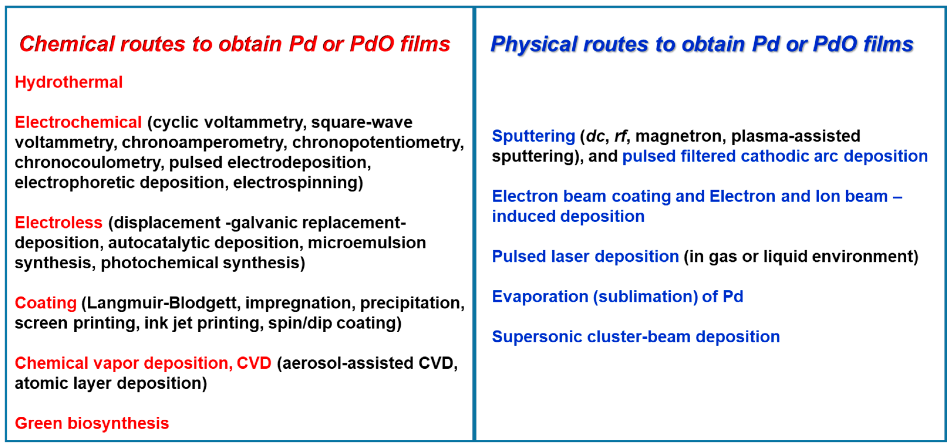
Figure 2.
Adapted from [98]. (a) Electrochemical gas sensor arrangement (30 mL glass cell): RE—reference electrode; MFC—mass flow controller and the inlet for the gas covered with fluorinated ethylene propylene (FEP) H2 gas-permeable membrane; WE—working electrode, PdO thin film of 1 μm thickness on ITO substrate; CE—counter electrode, Pt rod. (b) Room-temperature response by using the sensing arrangement from (a) when passing a H2 gas (10%–70% in Ar) into the cell for 200 s and for a constant potential on electrodes of 1 V.
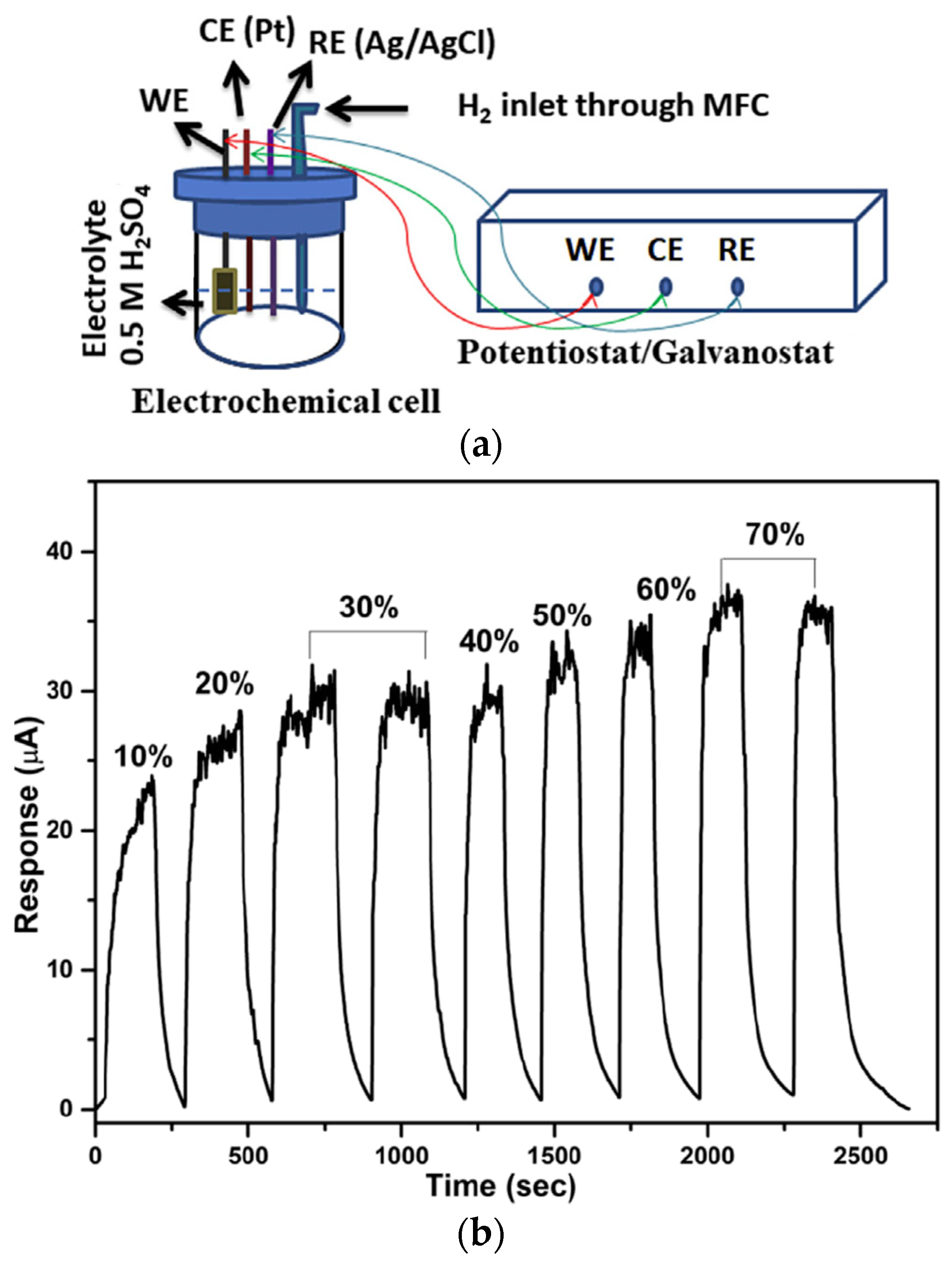
Figure 3.
Reproduced with permission from [106]. PdO sensor resistance at different ozone concentrations as a function of time at an operating temperature of 220 °C. SA denotes synthetic air. Note that ozone (O3) is harmful to human health, similar to other oxidizing gases, such as NOx, SO2, and Cl2. It is a by-product of many modern technologies, and its interaction under sunlight with volatile hydrocarbons produces many toxic organic compounds.
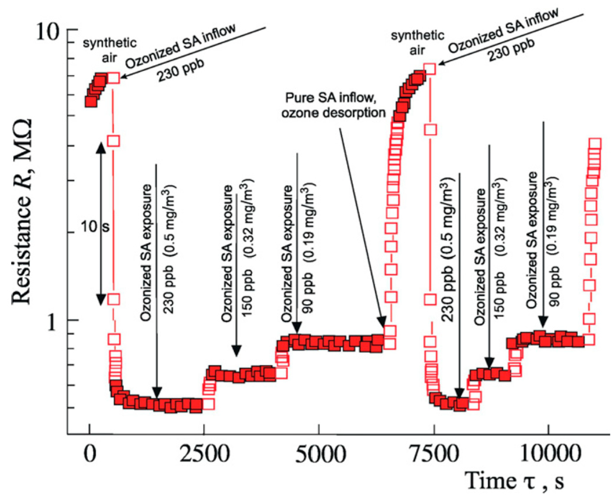
Figure 4.
Reproduced with permission from [121]. (i) TEM images taken on (a,b) ZnO and (c,d) ZnO-PdO. (ii) Response to toluene and ethanol of the structures from (i) at different operating temperatures.
Figure 4.
Reproduced with permission from [121]. (i) TEM images taken on (a,b) ZnO and (c,d) ZnO-PdO. (ii) Response to toluene and ethanol of the structures from (i) at different operating temperatures.
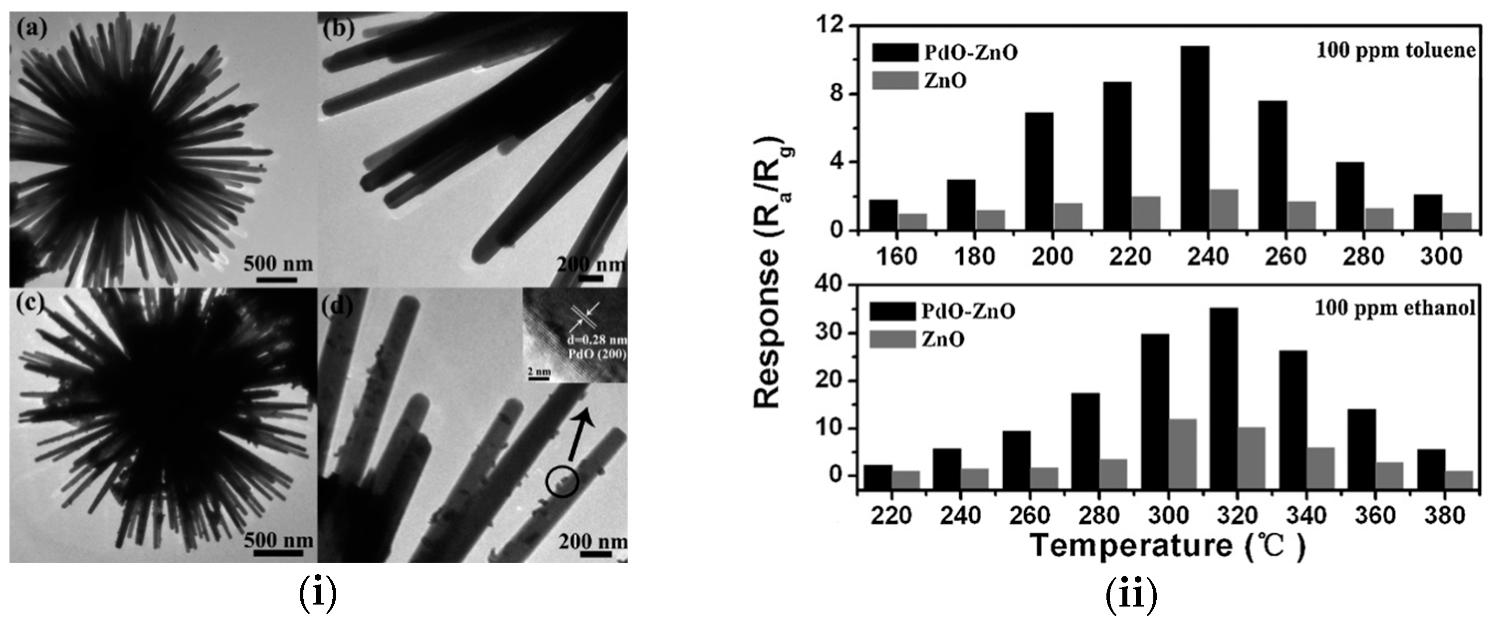
Figure 5.
Reproduced with permission from [124]. (a–c) SEM images of Pd/PdO films obtained by thermolysis in air, low vacuum, and N2. (d–f) SEM images of films from (a–c) were taken at higher magnification. (g–i) SEM images on cross-sections of the films from (a–c).
Figure 5.
Reproduced with permission from [124]. (a–c) SEM images of Pd/PdO films obtained by thermolysis in air, low vacuum, and N2. (d–f) SEM images of films from (a–c) were taken at higher magnification. (g–i) SEM images on cross-sections of the films from (a–c).

Figure 6.
Reproduced with permission from [167]. (a) SEM image of the porous Pd thin film on AAO substrate prepared by dc magnetron sputtering and post-annealed at 200 °C, and (b) room-temperature response at various hydrogen concentrations in nitrogen carrier gas. On the Pd film, Au electrodes (10 mm × 3 mm) were deposited by thermal evaporation.
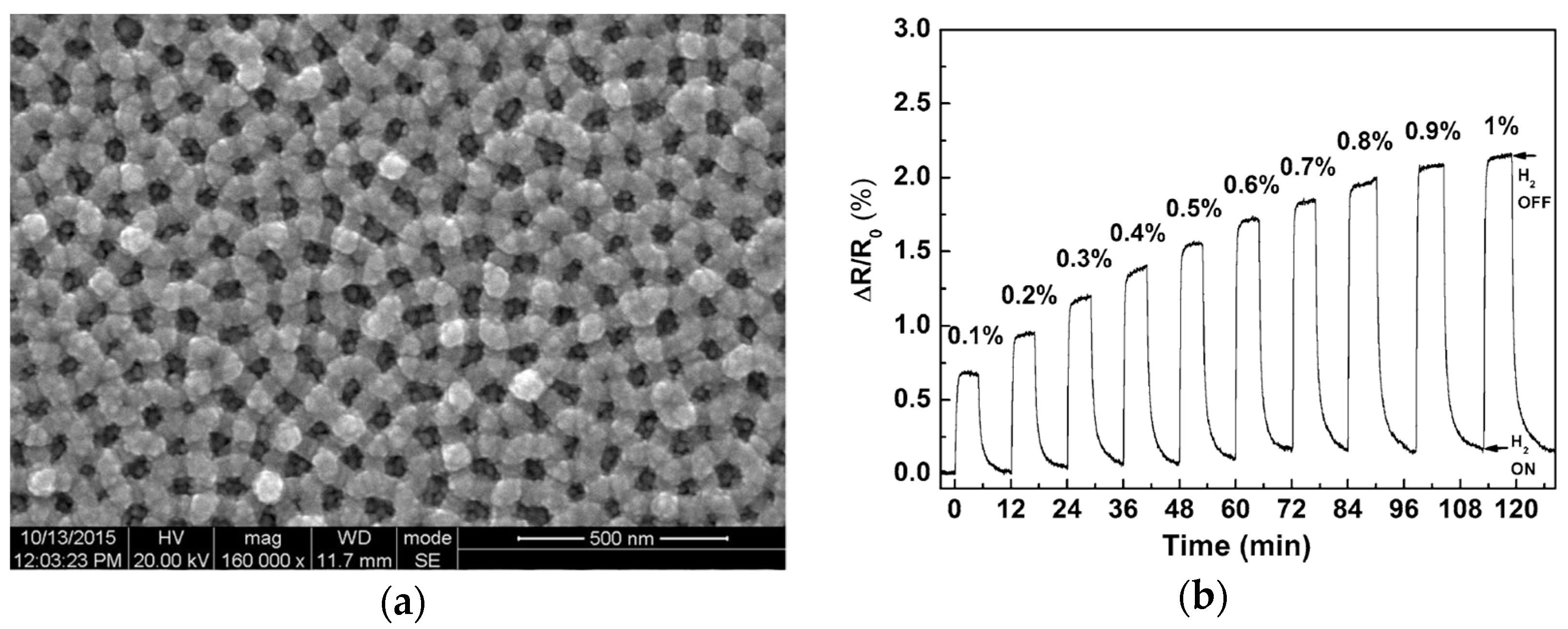
Figure 7.
Reproduced with permission from [176]. SEM images of reactively sputtered films in different oxygen atmospheres: (a) 15%, (b) 20%, (c) 25%, and (d) 30%.
Figure 7.
Reproduced with permission from [176]. SEM images of reactively sputtered films in different oxygen atmospheres: (a) 15%, (b) 20%, (c) 25%, and (d) 30%.

Figure 8.
Reproduced with permission from [185]. (a) Optical sensor arrangement based on optical absorbance of the sample when irradiated from a source of a halogen lamp in the spectral range of 400–800 nm. (b) Response time (calculated as the average time to change from 5% to 95% of the absorbance) at room temperature of the samples with different thicknesses to 5 vol.% H2 gas in nitrogen.
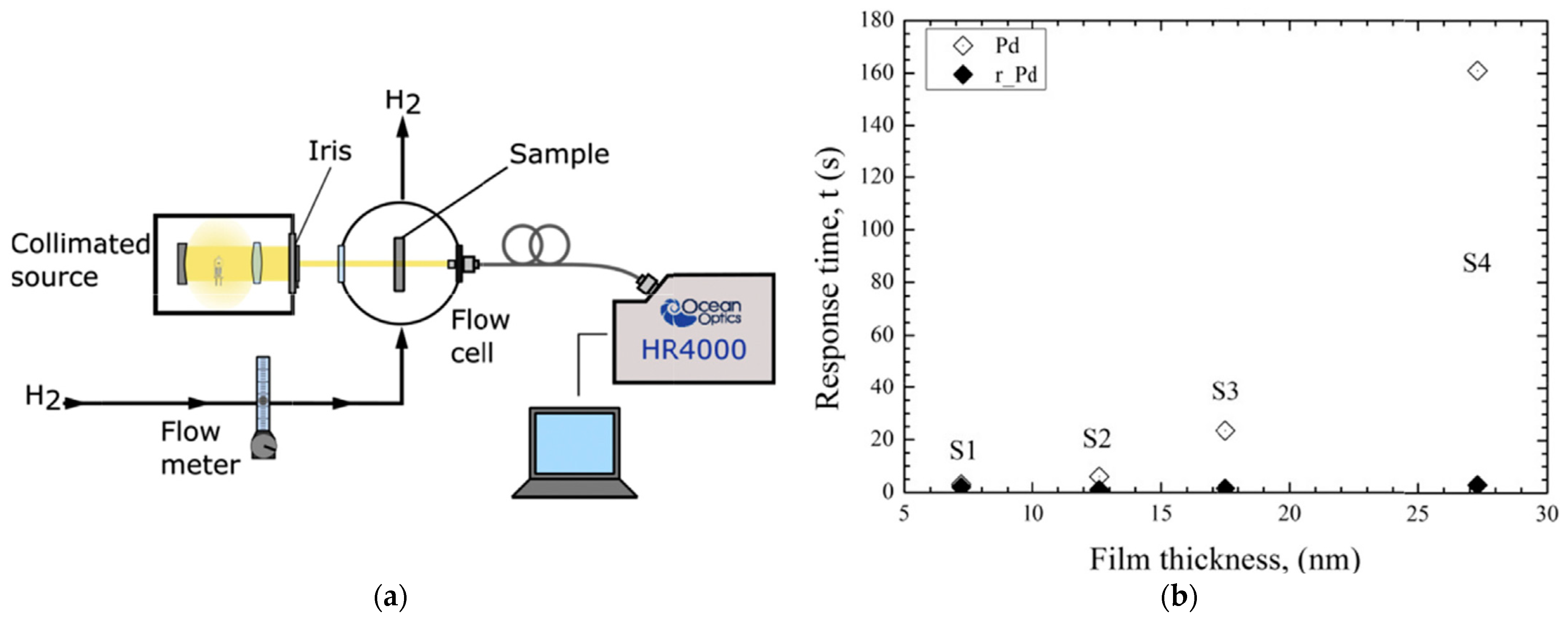
Figure 9.
Reproduced with permission from [225]. Fabrication of a typical Pd/MOS (MOS—metal oxide semiconductor) capacitor hydrogen sensor. The hydrogen diffuses from the metal Pd gate (active element) and creates a dipole layer at the (Pd/SiO2) interface that changes the work function of the active element. The response, R (%) = (CH − CN)/CN × 100, where CH and CN are the capacitance of the sensor in hydrogen gas and pure nitrogen, respectively. The carrier gas is nitrogen, argon, and air.
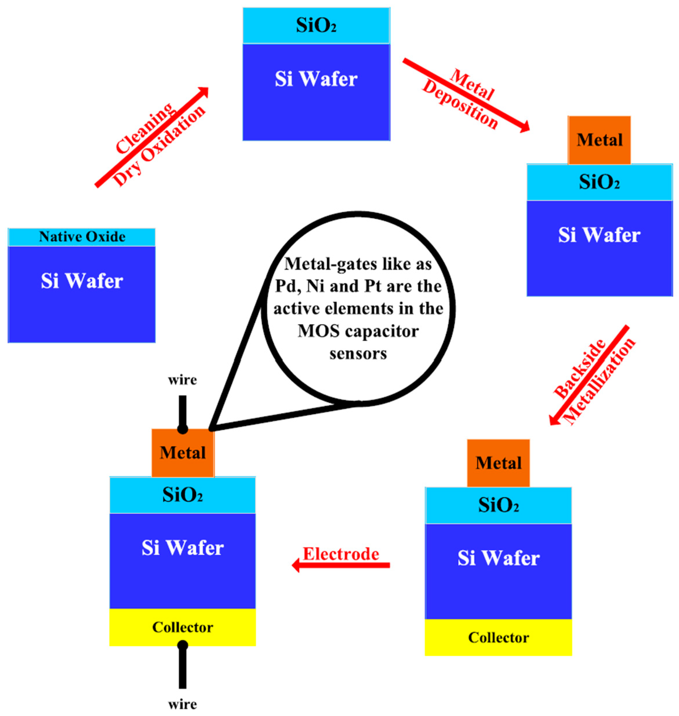
Figure 10.
Reproduced with permission from [245]. SEM images showing the morphology of Ir(1−x)PdxOy films deposited on 316 SS substrates for: (a) x = 0.14, (b) x = 0.50, (c) x = 0.90, and (d) x = 0.95. Map of morphology summarizing results from (a–d) depending on the composition of the Ir(1−x)PdxOy films (e).
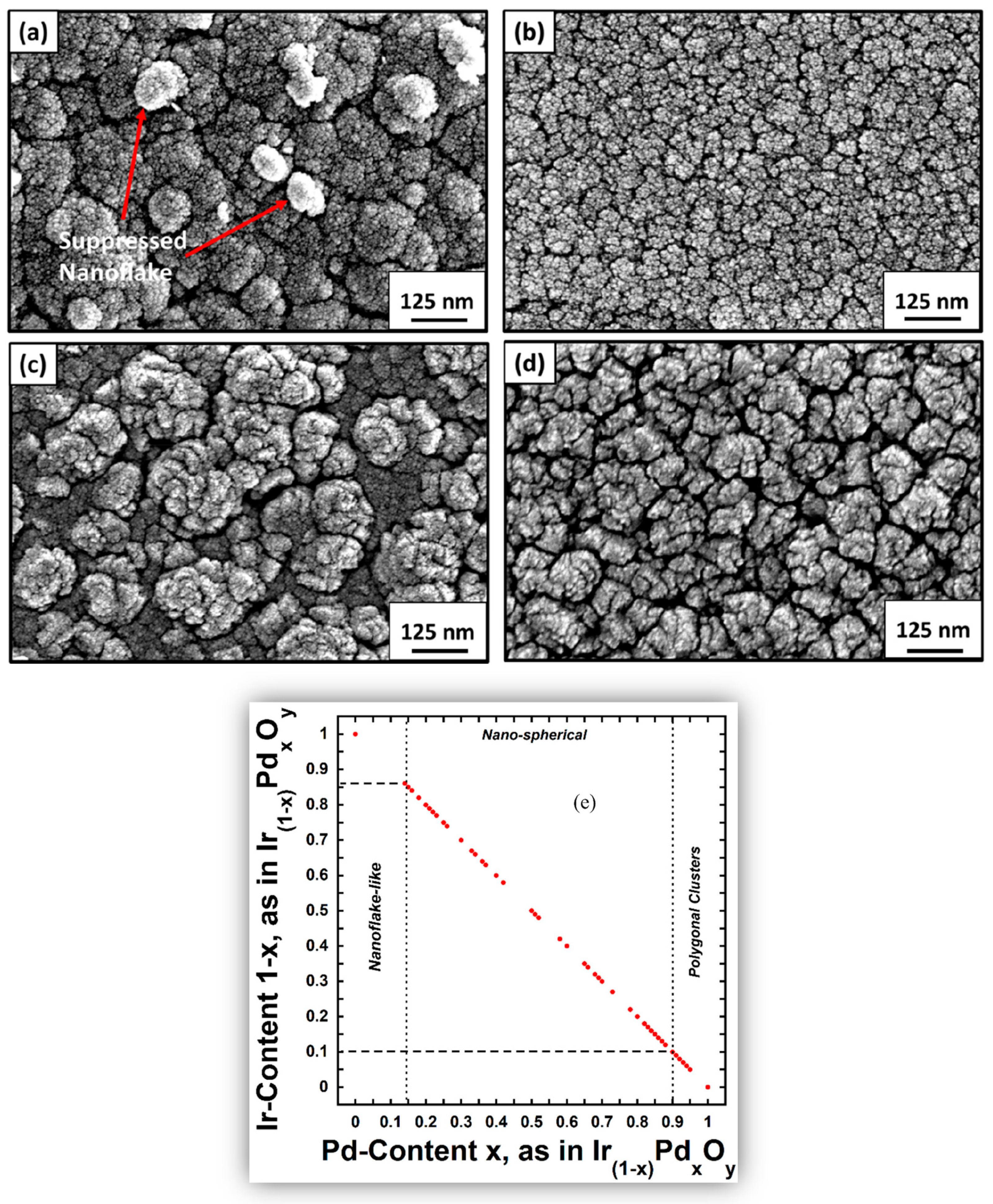
Disclaimer/Publisher’s Note: The statements, opinions and data contained in all publications are solely those of the individual author(s) and contributor(s) and not of MDPI and/or the editor(s). MDPI and/or the editor(s) disclaim responsibility for any injury to people or property resulting from any ideas, methods, instructions or products referred to in the content. |
© 2024 by the authors. Licensee MDPI, Basel, Switzerland. This article is an open access article distributed under the terms and conditions of the Creative Commons Attribution (CC BY) license (https://creativecommons.org/licenses/by/4.0/).
Share and Cite
MDPI and ACS Style
Badica, P.; Lőrinczi, A. A Review on Preparation of Palladium Oxide Films. Coatings 2024, 14, 1260. https://doi.org/10.3390/coatings14101260
AMA Style
Badica P, Lőrinczi A. A Review on Preparation of Palladium Oxide Films. Coatings. 2024; 14(10):1260. https://doi.org/10.3390/coatings14101260
Chicago/Turabian StyleBadica, Petre, and Adam Lőrinczi. 2024. "A Review on Preparation of Palladium Oxide Films" Coatings 14, no. 10: 1260. https://doi.org/10.3390/coatings14101260
Note that from the first issue of 2016, this journal uses article numbers instead of page numbers. See further details here.