Article

Temperature-Controlled and Adjustable Terahertz Device Based on Vanadium Dioxide

1
College of Technology, Hubei Engineering University, Xiaogan 432000, China
2
Joint Laboratory for Extreme Conditions Matter Properties, Southwest University of Science and Technology, Mianyang 621010, China
3
College of Physics, Central South University, Changsha 410083, China
*
Author to whom correspondence should be addressed.
Coatings 2024, 14(4), 478; https://doi.org/10.3390/coatings14040478
Submission received: 22 February 2024 / Revised: 5 April 2024 / Accepted: 10 April 2024 / Published: 13 April 2024
(This article belongs to the Special Issue Micro-Nano Optics and Its Applications)

Abstract

:
We propose a simple multifunctional terahertz absorber based on the simulation. The device consists of a gold layer, a SiO2 dielectric layer, and a VO2 top layer. The modulation mechanism of this device is to utilize the thermally induced phase transition characteristics of vanadium dioxide material. The simulation results show that when the temperature is 312 K, the device has the effect of complete reflection of terahertz waves. When the temperature is 345 K, the device has almost perfect absorption of terahertz wave in the range of 4.7–9.7 THz, and the spectral absorptivity is modulated in the range of 0~0.999. The electric field conditions at different temperatures were plotted to further explain the reasons for the performance transition of the device. The terahertz device was explained using impedance matching theory. In addition, the influence of different structural parameters on absorption rate was studied, providing reference for practical applications. At the same time, the device is polarization-insensitive and insensitive to the incident angle. When the incident angle changes from 0°to 45°, the device still has a stable absorption effect. The device has great application prospects in terahertz stealth, modulation, and other fields and provides ideas for the design of related devices.

1. Introduction

Terahertz wave refers to the electromagnetic wave with the frequency of 0.1–10 THz. Terahertz wave has the characteristics of low photon energy, short pulse, and strong penetrability and has broad application prospects. Terahertz absorption has unique advantages in communications, imaging, astronomy, radar, defense, medical, detection, etc., so it is now necessary for the development of terahertz technology. For example, terahertz can achieve wireless transmission rates of more than 10 Gbit/s in communication, which is impossible to achieve in microwave. And for the use of explosives in the terahertz band of different absorption spectra, terahertz can also detect and identify explosives [1,2,3,4]. However, most substances in nature are difficult to absorb terahertz wave by electromagnetic response with terahertz wave, which leads to the slow development of terahertz absorption devices [5,6]. However, since Landy et al. first proposed metamaterial absorbers in 2008, terahertz absorbers of corresponding structures have been extensively studied and rapidly developed [7]. This absorber is composed of a metal layer, dielectric layer, and metamaterial layer. It has the characteristics of simple structure, high absorptivity, thin thickness, and frequency selectivity. It has great applications in the fields of electromagnetic stealth [8], electromagnetic detection [9,10], biological detection [11], and sensing [12,13,14,15]. However, most metamaterial absorbers only work in a single wave band, with narrow absorption bandwidth, and are unable to achieve dynamic adjustment of absorption efficiency, which has great limitations and cannot be widely used [16,17,18,19]. Therefore, the design of a new terahertz absorber with wide absorption bandwidth, high absorption efficiency, dynamic adjustment of absorption efficiency, and wide application range has become a key research field. In recent years, due to the emergence of VO2 [20,21,22], graphene [23,24,25], liquid crystal [26,27], and other materials, the conductivity and dielectric properties of metamaterials can be changed by changing the physical conditions such as temperature, light, and electricity, so as to realize the dynamic adjustment of absorption rate.
VO2 is a phase-change material. When the temperature reaches about 340 K, its conductivity will change by four orders of magnitude. At this time, VO2 undergoes a reversible phase transition from an insulating phase to a metallic phase [28,29,30]. Therefore, devices designed using vanadium dioxide can achieve asymmetric transmission of electromagnetic waves, transmission of terahertz metasurface, and active tuning of terahertz waves by controlling temperature [31,32,33,34]. In 2018, Song et al. [35] achieved an absorption rate of over 90% in the absorption bandwidth range of 0.33 THz using a broadband tunable terahertz absorber based on vanadium dioxide metamaterial. In 2020, Huang et al. [36] designed an active controllable dual broadband terahertz absorber based on vanadium dioxide hybrid metamaterial, with an absorption rate exceeding 80% in the range of 0.56–1.44 THz and 2.88–3.65 THz. In 2020, Liu et al. [37] designed a dynamically tunable broadband terahertz absorber based on vanadium dioxide hybrid metamaterials, with an absorption rate of over 90% within the absorption bandwidth range of 1 THz. Although the above-mentioned absorbers realize the dynamic adjustment of the absorption rate by changing the temperature, there are still disadvantages such as narrow absorption bandwidth, small adjustment range, and insufficient absorption rate. Therefore, a broadband, high-absorption, dynamically tunable terahertz absorber is a feasible research direction.
In this paper, a terahertz regulator composed of VO2-SiO2-Au is designed based on theoretical simulation, which can perfectly absorb terahertz waves in the ultra wideband range of 4.7–9.7 THz. By changing the temperature, the phase transition of vanadium dioxide can be realized, and the device can convert between complete reflection and perfect absorption. When the temperature is 312 K, the device has the effect of complete reflection of terahertz wave. When the temperature is 345 K, the device has almost perfect absorption effect for terahertz wave in the range of 4.7–9.7 THz. At the same time, the device is insensitive to the incident angle. When the incident angle changes from 0° to 45°, the device still has a stable absorption effect. This makes the device have a wide range of applications and low limitations in practical applications. The terahertz modulator designed in this paper has great application potential in terahertz stealth, detection, filtering, thermal transmitter, modulation, and other fields and provides a new feasible scheme for related design.

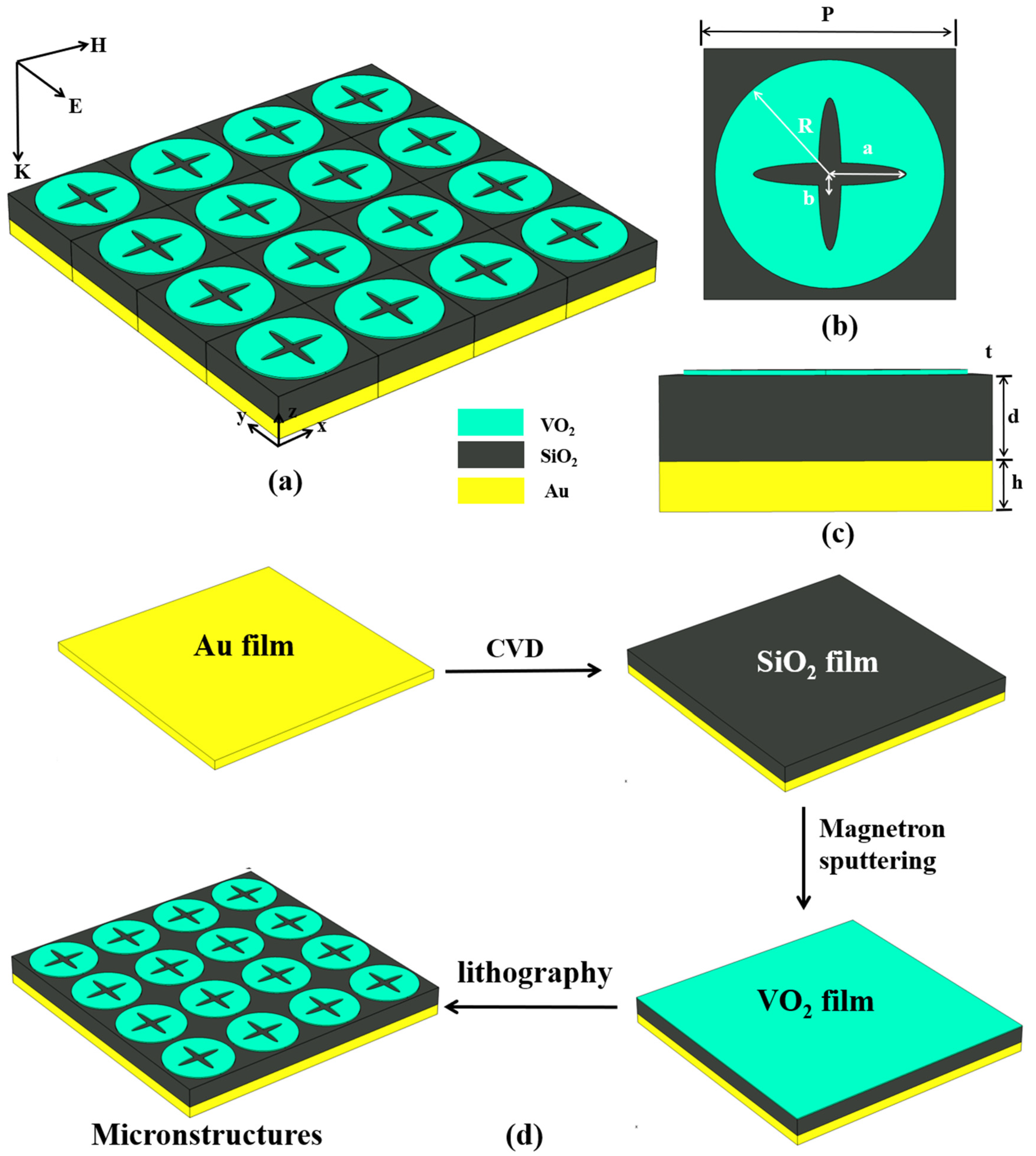
2. Structural Design and Analysis

The terahertz regulator structure proposed in this paper is a periodic structure, as shown in Figure 1. A representative prototype of the EM consists of three layers. The bottom reflecting layer is composed of gold film, whose thickness is much greater than the maximum skin depth of terahertz wave in gold, so that the transmissivity is 0, and the electromagnetic wave cannot penetrate. Therefore, the absorptance of our designed absorber can be approximated as A = 1−R, where R = |S11|2 [38,39,40]. The intermediate dielectric layer is composed of SiO2 with a dielectric constant of 2.13, which provides a transmission space and consumption path for terahertz waves incident on the absorber to dissipate in the absorber [41,42]. The surface resonance layer is composed of vanadium dioxide and has a specific pattern. Three-dimensional electromagnetic simulation software COMSOL was used to optimize the parameters and analyze the results. After optimization, the optimal structural parameters are as follows: P = 35 μm. R = 15.5 μm. a = 5 μm. b = 2 μm. h = 10 μm. d = 7.5 μm. t = 0.05 μm. The process flow of the regulating valve is given in Figure 1d. Firstly, sputtering creates a gold bottom layer 10 μm thick and 140 μm long and wide. Then, a SiO2 dielectric layer with a thickness of 7.5 μm and a length and width of 140 μm was generated by chemical vapor deposition; then, the top layer thickness of VO2 is 0.05 μm and a length and width of 140 μm was generated by magnetron sputtering; and finally, the surface layer was patterned by lithography. In this way, we use numerical simulation to theoretically guide the actual preparation of the THZ device, which has certain reference significance.
The Drude model allows characterization of the dielectric parameters of vanadium dioxide in the terahertz band, as shown in Equation (1) [43]:
ε ( ω ) V O 2 = ε ω P 2 ω ( ω + i γ )
ω P 2 = σ σ 0 ω P 0 2
Here, ε is the dielectric parameter at a high frequency, which has a value of 12, and ω P is the plasma frequency related to conductivity, as illustrated in Equation (2). The initial value of the plasma frequency is ω P 0 = 1.45 ×   10 15   s 1 , σ 0 = 3 ×   10 5   S m 1 , and the collision frequency γ = 5.75 × 10 13   s 1 . The conductivity σ will vary with the phase change of the vanadium dioxide film. From the relationship between the dielectric constant and the conductivity of the material, we are able to obtain the relational equation for the conductivity of vanadium dioxide films at various temperatures in the phase transition process, as shown in Equation (3) [44].
σ = i ε 0 ω ( ε c 1 )
Here, σ denotes the conductivity of the composite system, and ε 0 represents the dielectric constant in a vacuum. ε c is a temperature-dependent function.

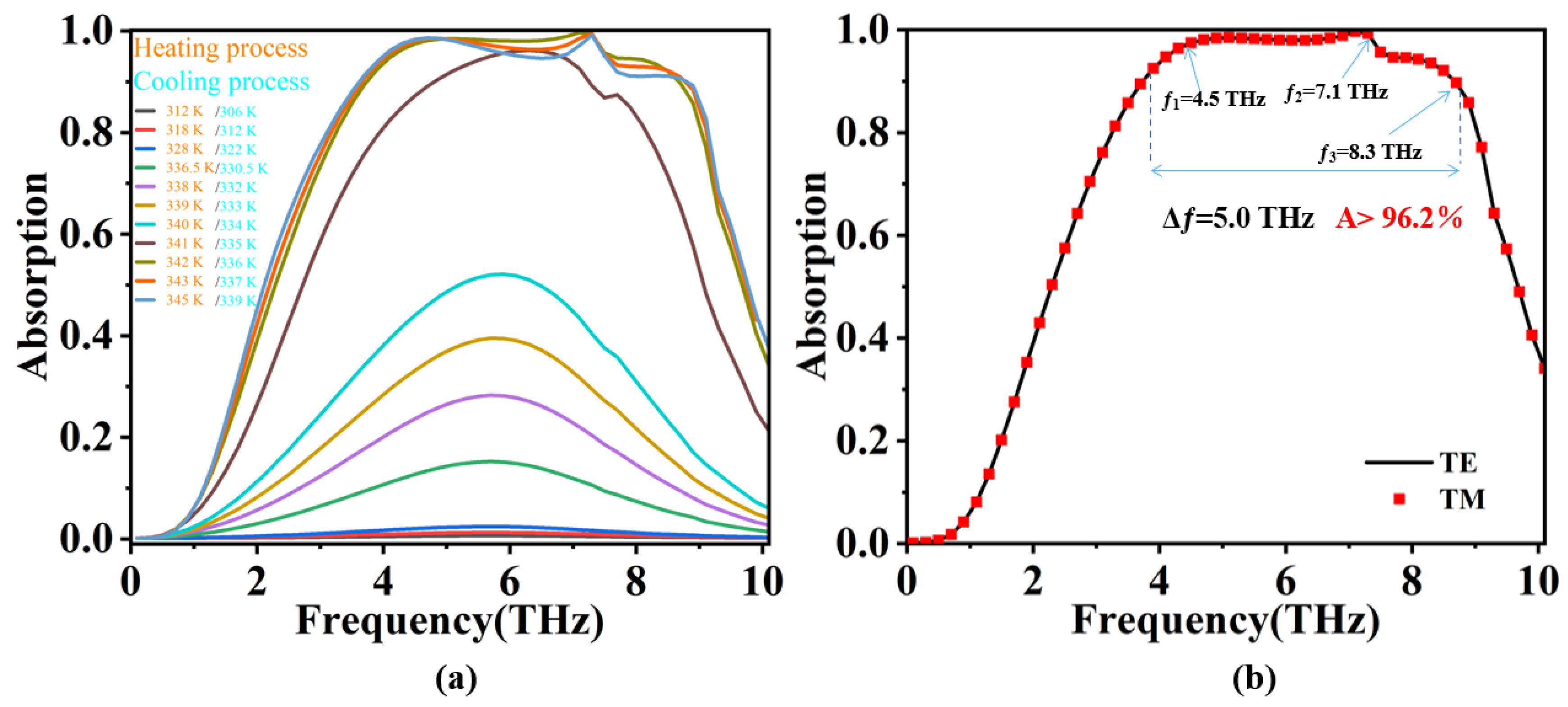
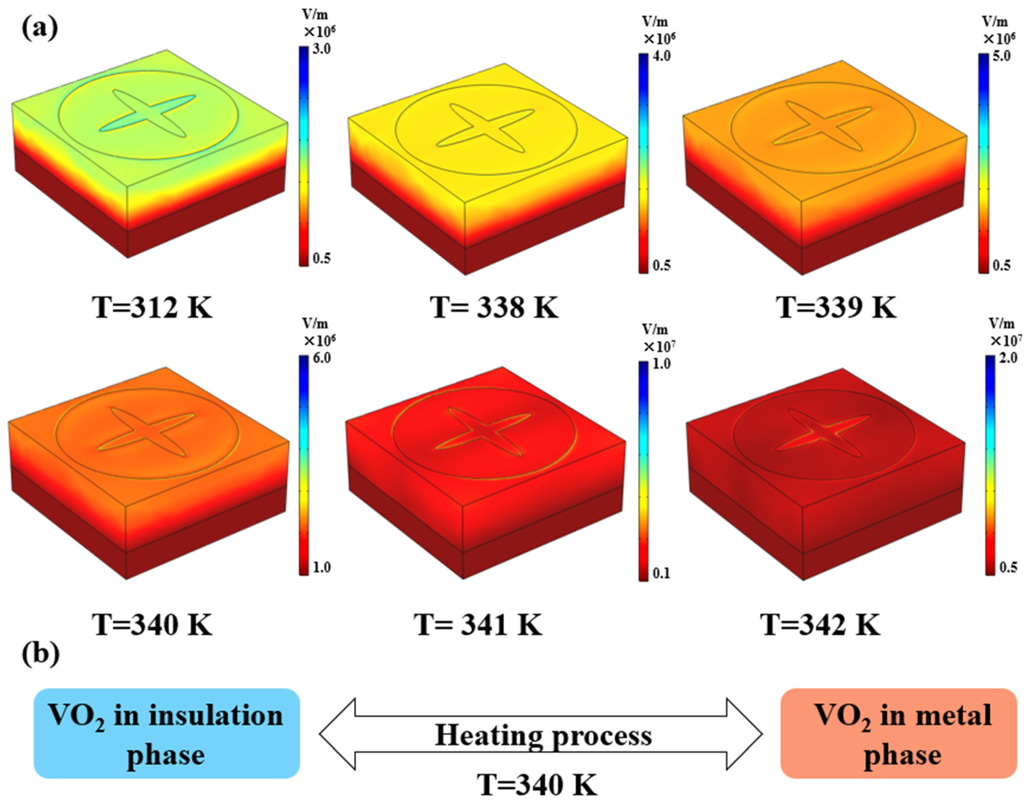
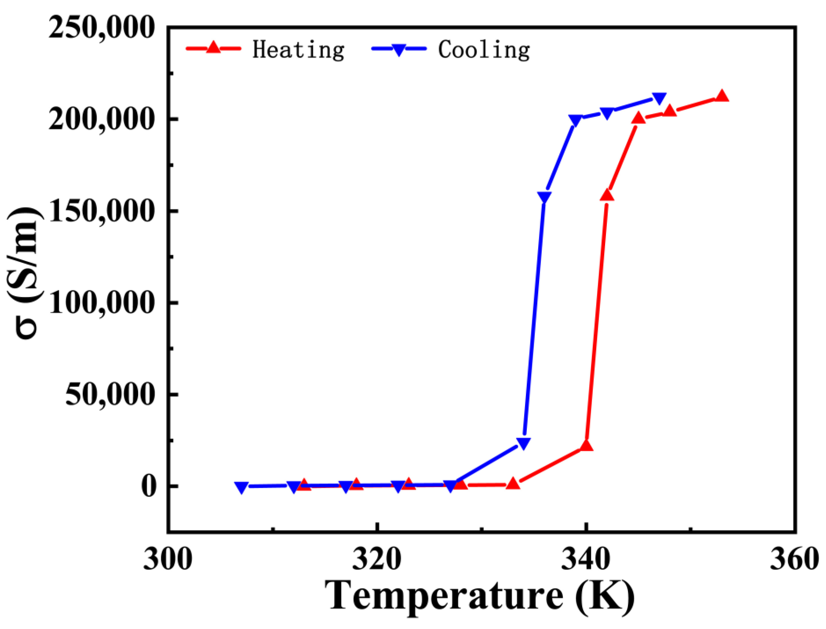
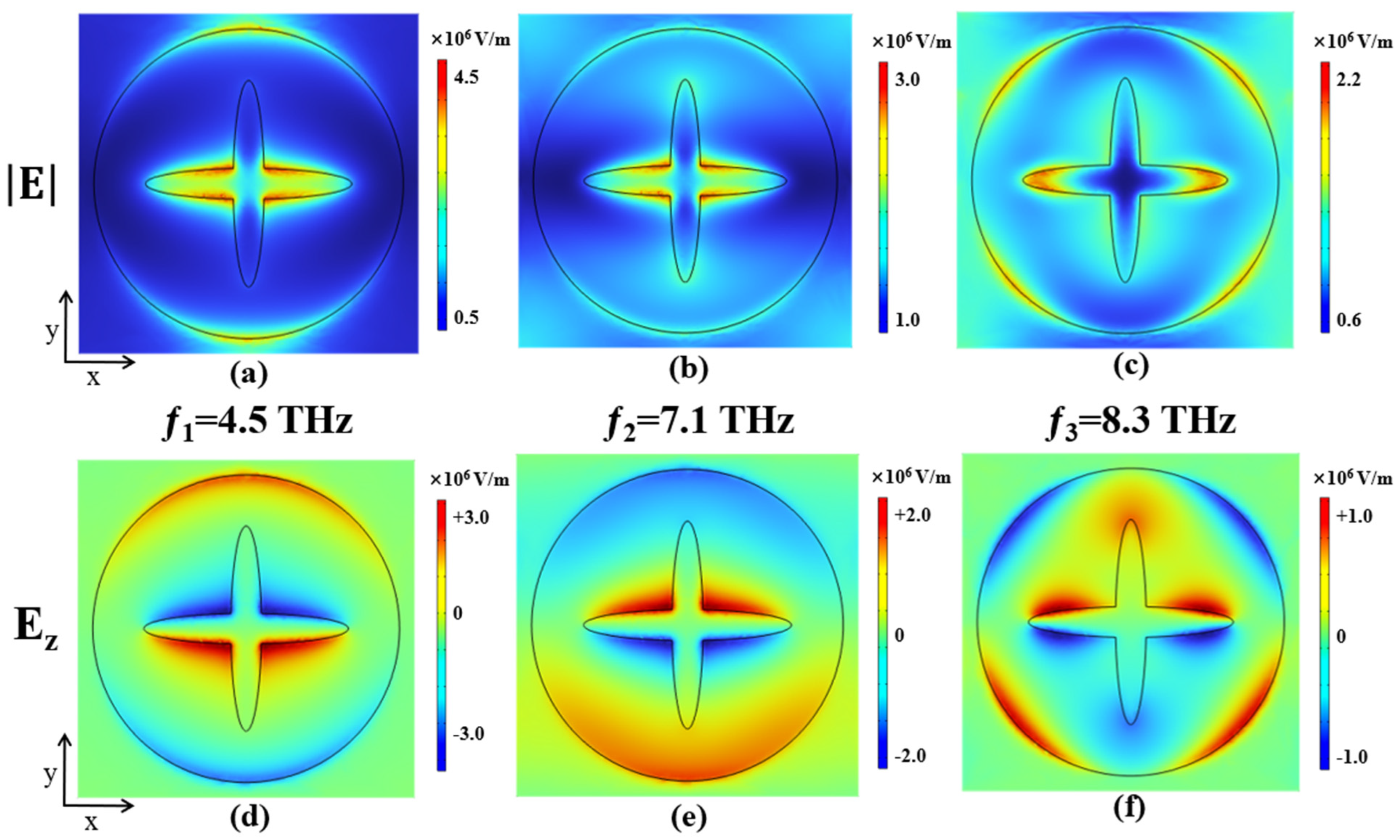
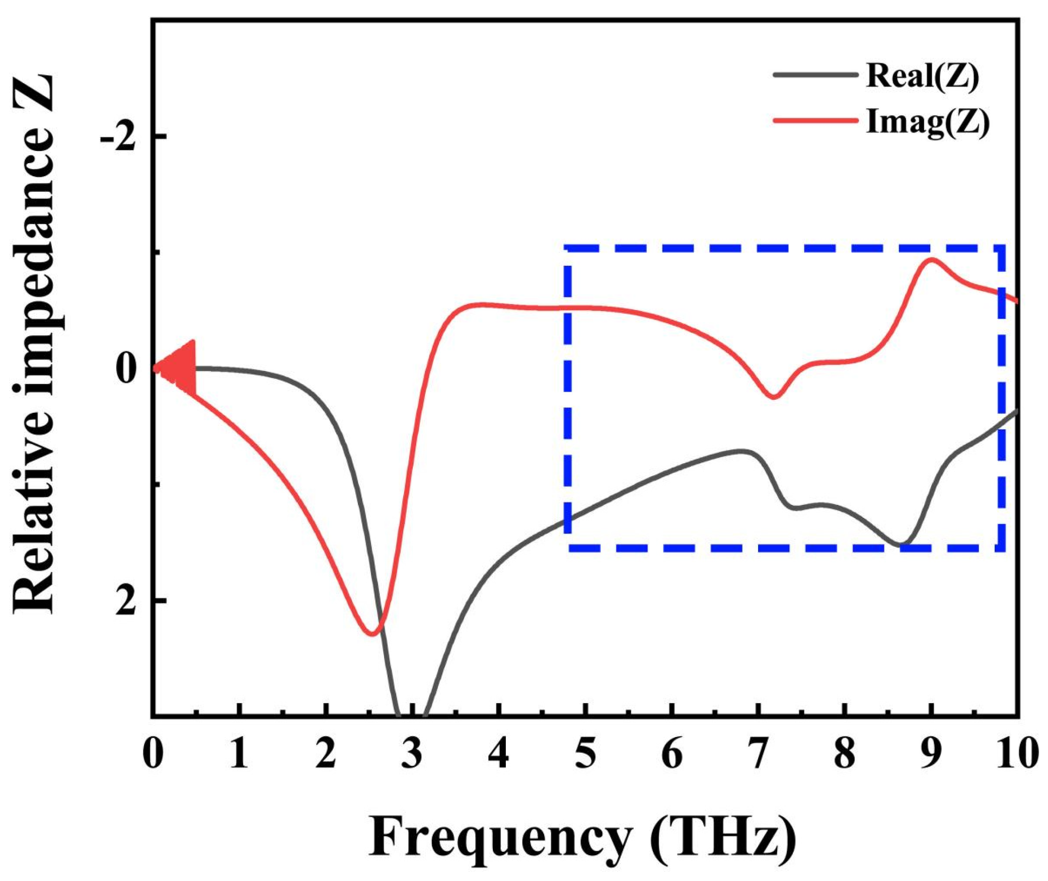
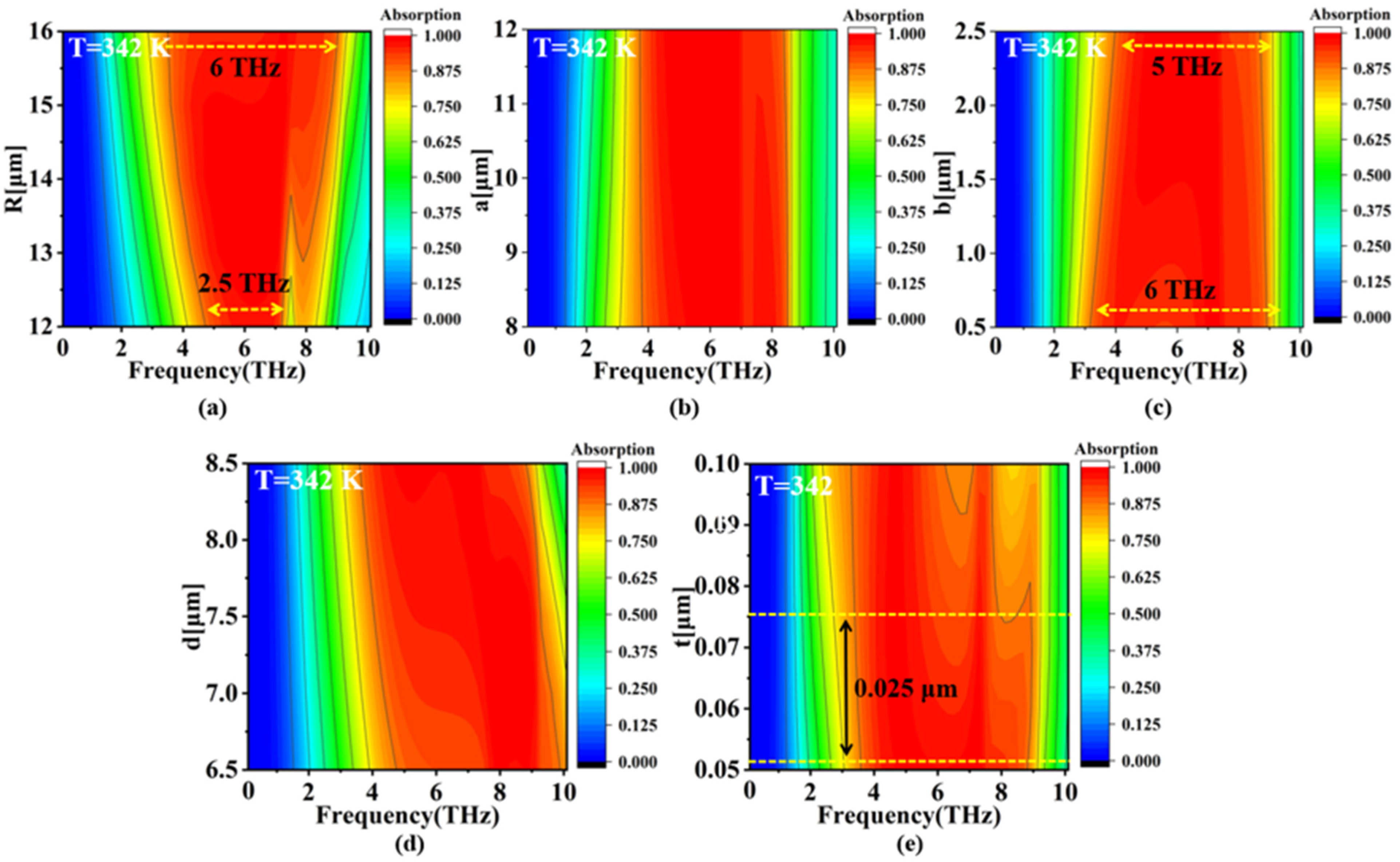
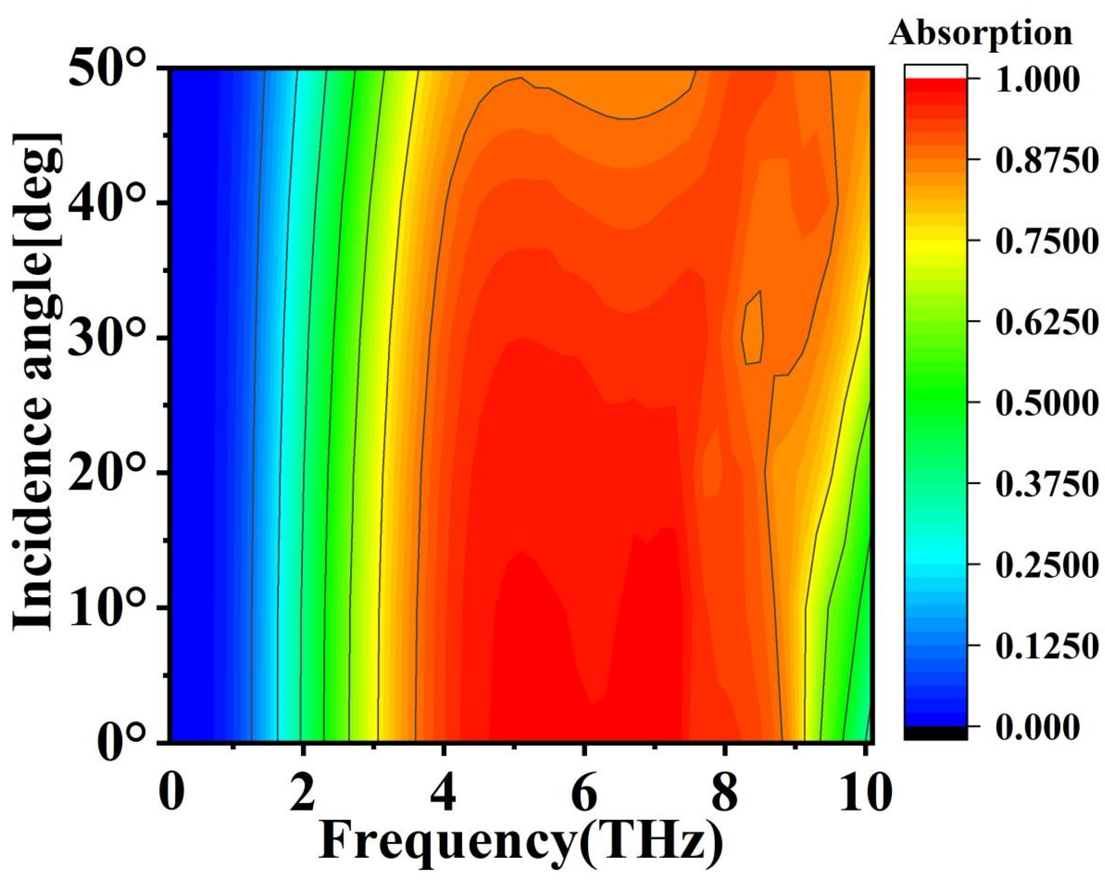
3. Results and Discussions

Through the simulation software, the absorption spectra of the regulator in the heating process (312 K–345 K) and cooling process (306 K–339 K) were calculated. As shown in Figure 2a, the absorption performance of the regulator for terahertz waves can be adjusted by changing the temperature, and the spectral absorptivity is modulated in the range of 0~0.999. The device has a temperature lag of 6 K during heating and cooling, which shows good memory, and the performance of the device can still maintain a controllable state. The performance of the device is discussed and analyzed below using the heating process.
Since A + R = 1, when the temperature is low (312 K), we see that the absorption rate of the device is almost 0, so the regulator shows a complete reflection of electromagnetic waves. As the temperature increases, the absorption capacity increases continuously. When T = 345 K, the device achieves near perfect absorption in the ultra wideband range of 3.7–8.7 THz. In addition, as shown in Figure 2b, in TE and TM modes, the absorption spectral curve of the regulator to terahertz wave is almost completely coincident, this is due to the high symmetry of the device [45], which makes the device polarization insensitive.
In order to explore the performance transition of the regulator (full reflection broadband absorbs perfectly), the electric field intensity distribution of the device during the heating process (TE mode, f = 7.1 THz; vertical incidence) was plotted. As shown in Figure 3a, the electric field intensity gradually increases with the increase of temperature. And then, the electric field intensity increases slowly in the range of 312~340 K. However, when the temperature exceeds 340 K, the electric field intensity increases rapidly, and its order of magnitude increases from 106 V/m to 107 V/m. This is caused by the phase transition of the top VO2 film at this time and the transformation of the internal structure [46], as shown in Figure 3b. In the process of vanadium dioxide thermally induced phase transition, with the increase in temperature, some scattered metal phase transition points begin to appear in the vanadium dioxide film, and these metal phase transition points will gradually diffuse with the increase in external temperature, forming a large metallic region, and finally covering the entire film [47]. In the process of vanadium dioxide thermally induced phase transition, the VO2 film is the coexistence of the insulating phase and metal phase. At the same time, the spatial heterogeneity of vanadium dioxide phase transition has a very strong impact on its macro dielectric properties. In this phase transition process, VO2 films have different electromagnetic responses to terahertz waves, which will affect the overall absorption effect of the device.
When the temperature rises to about 340 K, the internal crystal structure of vanadium dioxide film changes from an insulating state to a metallic state, and the change of crystal structure leads to a huge mutation in the photoelectric properties of vanadium dioxide [48]. VO2 conductivity has changed up to four orders of magnitude, as shown in Figure 4. The conductivity of vanadium dioxide is 100 S/m and 158,000 S/m at T = 312 K and T = 342 K, respectively. In practice, there may be some deviation due to humidity, oxidation, impurity doping, and other factors. VO2 can be considered an insulator or a metal at two temperatures. The corresponding device structure can be considered as a metal-dielectric-insulator (MDD) and metal-dielectric-metal (MDM). Among them, a MDD cannot form an effective resonant cavity, so that the terahertz wave incident on the surface is almost completely reflected, achieving the effect of high reflection. MDM is a classical resonant cavity, which can resonate the electromagnetic wave at a specific frequency and produce high absorption [49,50]. In fact, the surface plasmon resonance (SPR) caused by the matching of the frequency of the device structure and the frequency of terahertz wave is the reason for the high absorptivity of the device. At the same time, according to the above phenomenon, the influence of higher-order diffraction can also be excluded. Therefore, this structure can make the regulator convert between the perfect reflection effect and the perfect absorption effect of ultra wideband by adjusting the temperature, which has a broader application prospect. The mechanism of broadband absorption at T = 345 K (MDM structure) will be discussed in detail below.
In order to explore the broadband absorption mechanism at T = 345 K (MDM structure), the electric field distribution of the device at T = 345 K (vanadium dioxide in metal state) under three absorption peaks (ƒ1, ƒ2, ƒ3) was plotted, and the electric field of the incident light was polarized along the Y direction. As can be seen from Figure 5a,b,d,e, the electric field intensity distribution is particularly strong in the polarization direction, mainly distributed on the upper and lower sides of the vanadium dioxide disk and the edge of the elliptical frame in the X direction. This local electric field enhancement is due to the matching of the frequency of the vanadium dioxide resonant structure and the terahertz frequency, which causes the localized surface plasmon resonance [51,52]. In fact, the perfect absorption phenomenon at two frequencies is the result of resonance [53]. When the resonance occurs, the energy of the incident wave is tightly bound around the near-field of the VO2 structure and gradually dissipated by the structure of VO2 and the underlying gold film, forming nearly 100% perfect absorption. In addition, it can be seen that the electric field intensity distribution at the frequencies of ƒ1 and ƒ2 are almost the same. This indicates that the resonances of f1 mode and f2 mode are the same or similar. From Figure 5c,f, it can be seen that the phenomenon of local electric field enhancement on the elliptical structure also exists in the Y direction, and the local field enhancement on the disk becomes distributed on both sides of the Y direction. This indicates that the complete absorption in the f3 mode is caused by the plasmon resonance there, which is mainly related to the resonant structure composed of the elliptical structure in the Y direction and the oblique edge part of the disk [54]. These three resonance modes are all localized surface plasmon resonance phenomena in nature. The structure frequency of the device designed in this paper can match the frequency of terahertz wave in a wide range, which is the cause of broadband absorption.
In addition, we also calculate the relative impedance Z. We know that when the equivalent impedance of the absorber matches the impedance of the free space, the relative impedance Z = 1, the device will reach the critical coupling condition, thus showing strong electromagnetic absorption characteristics. The expression of the relative impedance Z is as follows [55,56]:
Ζ = ± 1 + S 11 2 S 21 2 1 S 11 2 S 21 2
Figure 6 shows the real and imaginary parts of the relative impedance of the absorber in the operating interval. At the beginning, the real part of the impedance of the device is relatively dense. Then we can see that in the blue box that the real part of the relative impedance of the device is close to 1, and the imaginary part is close to 0 (T = 345 K) in the range of good absorption benefit. This indicates that the reflection of the system is well suppressed, corresponding to a perfect absorption state. The numerical simulation results in Figure 6 are in agreement with the theoretical results, which proves that the perfect absorption occurs in the range of 3.7–8.7 THz.
In the above discussion, the performance of the device under ideal conditions was calculated and analyzed. But in the actual production process, the structural parameters and production process, often errors appear [57,58]. These issues will have a certain impact on the performance of the device in practical applications, and errors in production processes can also have a certain impact on the performance of the device. The following will discuss and analyze the various structural parameters of the regulator and explore their impact on performance. From Figure 7a–c, it can be seen that the structural parameters play a major role in the top VO2 pattern, with the radius R being the most prominent. As R increases, the absorption bandwidth and intensity gradually increase from 9 to 12 μm. The spectrum corresponding to the length of the ellipse within the range of m remains almost unchanged, and the absorption spectrum corresponding to the width b of the ellipse only experiences some bandwidth reduction. This is because as the size of VO2 changes, the original resonant unit on it is destroyed, causing a mismatch with the external terahertz wave frequency, and it is unable to excite the resonant mode at this frequency. The most prominent reason for the influence of radius R is that R is the dominant parameter of the size of the VO2 structure, and an increase or decrease in R can cause the distribution and generation of small resonant units on the VO2 structure. The thickness h of the intermediate medium layer and the thickness t of the top absorption layer are two crucial parameters that have a significant impact on the performance of the regulator. From Figure 7d, it can be seen that as d increases, the absorption bandwidth remains almost unchanged, but the absorption range undergoes a significant red shift. As can be seen from Figure 7e, the device can maintain good performance when the thickness of VO2 is within the range of 50–75 nm. Then with the increase of its thickness, the absorption rate at the high frequency decreases gradually. This provides an effective direction and approach for adjusting the operating frequency range of the device [59,60].
Finally, we must consider that terahertz waves transmitted in actual space may not always interact with the device in a normal incidence form but may also be incident from other different directions. Therefore, it is necessary to design devices with wide-angle characteristics [61,62]. This feature is of great significance for practical applications. The device structure obtained through continuous adjustment of structural parameters, geometric patterns, and simulation optimization has high environmental adaptability, as shown in Figure 8. From Figure 8, it can be seen that when the incident angle changes within the range of 0°–45°, the absorption performance remains almost unchanged and can still maintain a high absorption of 5 THz ultra wideband. However, as the incidence angle continues to increase, the absorption effect begins to decline. This can be understood as the energy of the incident electromagnetic field in the intermediate medium decreasing as the angle increases, and the strong electric magnetic resonance cannot be effectively driven (in the case of oblique incidence, only some resonance units are excited or no units are excited) [63]. Overall, the device can still maintain excellent performance over a wide angle range. This means that this design can maintain flexible application in practice. Additionally, our structure is very simple. The design consists of only three layers, with a simple structure and easy processing and production. In addition, the designed device can not only achieve perfect absorption and complete reflection function switching but also greatly improve the absorption performance. At a temperature of 345 K, the absorption bandwidth reaches an astonishing 5.0 THz, which spans half the terahertz band, while its average absorption rate is still above 96.2%. Table 1 shows a comparison between our work and existing ones [64,65,66,67,68,69]. From the table, we can see that our work has certain advantages in many aspects.
We conducted a comparative analysis of several terahertz absorbers/reflectors. As depicted in the table, our notable advantages lie in possessing a broader absorption spectrum and higher absorption efficiency. The incorporation of vanadium dioxide endows our terahertz absorber with the capacity for absorption modulation. Compared to metamaterials and semiconductor materials, vanadium dioxide’s property modulation in response to temperature changes enhances its adjustability for the device. In this study, we achieved nearly dynamic modulation of absorption from 0 to 1, spanning over half of the terahertz band. However, it is crucial to note that our device maintains a bandwidth of 5 THz (greater than 90%) only within a 45° range, necessitating attention in practical applications.

4. Conclusions

This article designs a terahertz regulator with a simple structure and diverse functions. It is composed of a three-layer structure consisting of a gold substrate, a SiO2 dielectric layer, and a VO2 top layer and is easy to process. After simulation verification, the changes in electric field intensity observed at different temperatures confirm that the regulatory mechanism is derived from the temperature-induced phase transition characteristics of vanadium dioxide materials. The absorption mechanism of the device is also explained by impedance matching theory. In addition, research has shown that the device has a complete reflection effect on terahertz waves at a temperature of 312 K. At a temperature of 345 K, the device exhibits almost perfect absorption of terahertz waves in the range of 4.7 to 9.7 THz. Due to the high symmetry of the device structure and its polarization independence, the designed regulator is polarization insensitive. At the same time, the device is not sensitive to the incidence angle and maintains relatively stable absorption characteristics within the range of 0°–45° incidence angle. Based on the above advantages, the terahertz regulator designed in this article has significant application potential in terahertz stealth, detection, filtering, thermal emitters, modulation, and other fields.

Author Contributions

Conceptualization, W.L., H.S. and W.X.; data curation, W.L., H.S., W.X. and Y.D.; formal analysis, W.L. and Y.Y.; methodology, H.S., W.X., Y.D. and Y.Y.; resources, W.X.; software, W.L., H.S., W.X., Y.D. and Y.Y.; data curation, W.X.; writing—original draft preparation, W.L.; writing—review and editing, W.L., H.S., W.X., Y.D. and Y.Y. All authors have read and agreed to the published version of the manuscript.

Funding

The authors are grateful to the support by the Hubei Provincial Higher Education Provincial Teaching Research Project (2022551); Funded by the Second Batch of Ministry of Education’s Collaborative Education Projects between Industry and Academia (202102198004); Funded by the Hubei Provincial Department of Education Science and Technology Research Project (B2022507).

Institutional Review Board Statement

Not applicable.

Informed Consent Statement

Not applicable.

Data Availability Statement

Publicly available datasets were analyzed in this study. These data can be found here: [https://www.lumerical.com/ (accessed on 1 January 2020)].

Conflicts of Interest

The authors declare no conflicts of interest.

References

  1. Chataut, R.; Nankya, M.; Akl, R. 6G Networks and the AI Revolution—Exploring Technologies, Applications, and Emerging Challenges. Sensors 2024, 24, 1888. [Google Scholar] [CrossRef] [PubMed]
  2. Li, W.X.; Zhao, W.C.; Cheng, S.B.; Yang, W.X.; Yi, Z.; Li, G.F.; Zeng, L.C.; Li, H.L.; Wu, P.H.; Cai, S.S. Terahertz Selective Active Electromagnetic Absorption Film Based on Single-layer Graphene. Surf. Interfaces 2023, 40, 103042. [Google Scholar] [CrossRef]
  3. Yu, Z.Q.; Zhang, N.; Wang, J.X.; Dai, Z.J.; Gong, C.; Lin, L.; Guo, L.; Liu, W. 0.35% THz pulse conversion efficiency achieved by Ti:sapphire femtosecond laser filamentation in argon at 1 kHz repetition rate. Opto-Electron. Adv. 2022, 5, 210065. [Google Scholar] [CrossRef]
  4. Zhang, R.Y.; Luo, Y.H.; Xu, J.K.; Wang, H.Y.; Han, H.Y.; Hu, D.; Zhu, Q.F.; Zhang, Y. Structured vanadium dioxide metamaterial for tunable broadband terahertz absorption. Opt. Express 2021, 29, 42989–42998. [Google Scholar] [CrossRef]
  5. Asif, M.; Wang, Q.; Ouyang, Z.; Lin, M.; Liang, Z. Ultra-Wideband Terahertz Wave Absorber Using Vertically Structured IGIGIM Metasurface. Crystals 2024, 14, 22. [Google Scholar] [CrossRef]
  6. Zheng, R.Y.; Liu, Y.H.; Ling, L.; Sheng, Z.X.; Yi, Z.; Song, Q.J.; Tang, B.; Zeng, Q.D.; Chen, J.; Sun, T.Y. Ultra wideband tunable terahertz metamaterial absorber based on single-layer graphene strip. Diam. Relat. Mater. 2024, 141, 110713. [Google Scholar] [CrossRef]
  7. Landy, N.I.; Sajuyigbe, S.; Mock, J.J. Perfect metamaterial absorber. Phys. Rev. Lett. 2008, 100, 207402. [Google Scholar] [CrossRef] [PubMed]
  8. Iwaszczuk, K.; Strikwerda, A.C.; Fan, K.; Zhang, X.; Averitt, R.D.; Jepsen, P.U. Flexible metamaterial absorbers for stealth applications at terahertz frequencies. Opt. Express 2012, 20, 635. [Google Scholar] [CrossRef]
  9. Lewis, R.A. A review of terahertz detectors. J. Phys. D Appl. Phys. 2019, 52, 433001. [Google Scholar] [CrossRef]
  10. Yalagala, B.P.; Dahiya, A.S.; Dahiya, R. ZnO nanowires based degradable high-performance photodetectors for eco-friendly green electronics. Opto-Electron. Adv. 2023, 6, 220020. [Google Scholar] [CrossRef]
  11. Gezimati, M.; Singh, G. Advances in terahertz technology for cancer detection applications. Opt. Quant. Electron. 2022, 55, 151. [Google Scholar] [CrossRef] [PubMed]
  12. Ma, J.; Wu, P.H.; Li, W.X.; Liang, S.R.; Shangguan, Q.Y.; Cheng, S.B.; Tian, Y.H.; Fu, J.Q.; Zhang, L.B. A five-peaks graphene absorber with multiple adjustable and high sensitivity in the far infrared band. Diam. Relat. Mater. 2023, 136, 109960. [Google Scholar] [CrossRef]
  13. Khonina, S.N.; Kazanskiy, N.L.; Butt, M.A.; Karpeev, S.V. Optical multiplexing techniques and their marriage for on-chip and optical fiber communication: A review. Opto-Electron. Adv. 2022, 5, 210127. [Google Scholar] [CrossRef]
  14. Shangguan, Q.; Chen, Z.; Yang, H.; Cheng, S.; Yang, W.; Yi, Z.; Wu, X.; Wang, S.; Yi, Y.; Wu, P. Design of Ul-tra-Narrow Band Graphene Refractive Index Sensor. Sensors 2022, 22, 6483. [Google Scholar] [CrossRef] [PubMed]
  15. Cozzolino, F.; Marra, F.; Fortunato, M.; Bellagamba, I.; Pesce, N.; Tamburrano, A.; Sarto, M.S. New Sensing and Radar Absorbing Laminate Combining Structural Damage Detection and Electromagnetic Wave Absorption Properties. Sensors 2022, 22, 8470. [Google Scholar] [CrossRef] [PubMed]
  16. Wang, D.Y.; Zhu, W.L.; Yi, Z.; Ma, G.L.; Gao, X.; Dai, B.; Yu, Y.; Zhou, G.R.; Wu, P.H.; Liu, C. Highly sensitive sensing of a magnetic field and temperature based on two open ring channels SPR-PCF. Opt. Express 2022, 30, 39056. [Google Scholar] [CrossRef] [PubMed]
  17. Khaled, A.; Arun, U.; Gaurav, S.; Arjuna, M.; Meshari, A.; Ammar, A. A theoretical analysis of refractive index sensor with improved sensitivity using titanium dioxide, graphene, and antimonene grating: Pseudomonas bacteria detection. Measurement 2023, 216, 112957. [Google Scholar] [CrossRef]
  18. Yue, Z.; Li, J.T.; Li, J.; Zheng, C.L.; Liu, J.Y.; Lin, L.; Guo, L.; Liu, W. Terahertz metasurface zone plates with arbitrary polarizations to a fixed polarization conversion. Opto-Electron. Sci. 2022, 1, 210014. [Google Scholar] [CrossRef]
  19. Gigli, C.; Leo, G. All-dielectric χ(2) metasurfaces: Recent progress. Opto-Electron. Adv. 2022, 5, 210093. [Google Scholar] [CrossRef]
  20. Wang, X.; Liu, Y.; Jia, Y.; Su, N.; Wu, Q. Ultra-Wideband and Narrowband Switchable, Bi-Functional Metamaterial Absorber Based on Vanadium Dioxide. Micromachines 2023, 14, 1381. [Google Scholar] [CrossRef]
  21. Liang, S.R.; Xu, F.; Li, W.X.; Yang, W.X.; Cheng, S.B.; Yang, H.; Chen, J.; Yi, Z.; Jiang, P.P. Tunable smart mid in-frared thermal control emitter based on phase change material VO2 thin film. Appl. Therm. Eng. 2023, 232, 121074. [Google Scholar] [CrossRef]
  22. Choi, S.B.; Kyoung, J.S.; Kim, H.S.; Park, H.R.; Park, D.J.; Kim, B.J.; Ahn, Y.H.; Rotermund, F.; Kim, H.T.; Ahn, K.J.; et al. Nanopattern enabled terahertz all-optical switching on vanadium dioxide thin film. Appl. Phys. Lett. 2011, 98, 071105. [Google Scholar] [CrossRef]
  23. Li, W.X.; Liu, M.S.; Cheng, S.B.; Zhang, H.F.; Yang, W.X.; Yi, Z.; Zeng, Q.D.; Tang, B.; Ahmad, S.; Sun, T.Y. Polar-ization independent tunable bandwidth absorber based on single-layer graphene. Diam. Relat. Mater. 2024, 142, 110793. [Google Scholar] [CrossRef]
  24. Kubacki, R.; Przesmycki, R.; Laskowski, D. Shielding Effectiveness of Unmanned Aerial Vehicle Electronics with Graphene-Based Absorber. Electronics 2023, 12, 3973. [Google Scholar] [CrossRef]
  25. Tang, C.J.; Nie, Q.M.; Cai, P.G.; Liu, F.X.; Gu, P.; Yan, Z.D.; Huang, Z.; Zhu, M.W. Ultra-broadband near-infrared absorption enhancement of monolayer graphene by multiple-resonator approach. Diam. Relat. Mater. 2024, 141, 110607. [Google Scholar] [CrossRef]
  26. Kanyang, R.; Fang, C.; Yang, Q.; Shao, Y.; Han, G.; Liu, Y.; Hao, Y. Electro-Optical Modulation in High Q Metasurface Enhanced with Liquid Crystal Integration. Nanomaterials 2022, 12, 3179. [Google Scholar] [CrossRef] [PubMed]
  27. Zhuang, X.; Zhang, W.; Wang, K.; Gu, Y.; An, Y.; Zhang, X.; Gu, J.; Luo, D.; Han, J.; Zhang, W. Active terahertz beam steering based on mechanical deformation of liquid crystal elastomer metasurface. Light. Sci. Appl. 2023, 12, 14. [Google Scholar] [CrossRef] [PubMed]
  28. Zheng, Z.P.; Luo, Y.; Yang, H.; Yi, Z.; Zhang, J.G.; Song, Q.J.; Yang, W.X.; Liu, C.; Wu, X.W.; Wu, P.H. Thermal tuning of terahertz metamaterial properties based on phase change material vanadium dioxide. Phys. Chem. Chem. Phys. 2022, 24, 8846–8853. [Google Scholar] [CrossRef]
  29. Xu, Z.Q.; Luo, H.; Zhu, H.Z.; Hong, Y.; Shen, W.D.; Ding, J.P.; Kaur, S.; Ghosh, P.; Qiu, M.; Li, Q. Nonvolatile optically reconfigurable radiative metasurface with visible tunability for anticounterfeiting. Nano Lett. 2021, 21, 5269–5276. [Google Scholar] [CrossRef]
  30. Zheng, L.; Feng, R.; Shi, H.; Li, X. Tunable Broadband Terahertz Metamaterial Absorber Based on Vanadium Dioxide and Graphene. Micromachines 2023, 14, 1715. [Google Scholar] [CrossRef]
  31. Liu, M.; Xu, Q.; Chen, X.; Plum, E.; Li, H.; Zhang, X.; Zhang, C.; Zou, C.; Han, J.; Zhang, W. Temperature-Controlled Asymmetric Transmission of Electromagnetic Waves. Sci. Rep. 2019, 9, 4097. [Google Scholar] [CrossRef] [PubMed]
  32. Serebryannikov, A.E.; Lakhtakia, A.; Vandenbosch, G.A.E.; Ozbay, E. Transmissive terahertz metasurfaces with vanadium dioxide split-rings and grids for switchable asymmetric polarization manipulation. Sci. Rep. 2022, 12, 3518. [Google Scholar] [CrossRef] [PubMed]
  33. Cakmak, A.O.; Colak, E.; Serebryannikov, A.E. Using Thin Films of Phase-Change Material for Active Tuning of Terahertz Waves Scattering on Dielectric Cylinders. Materials 2024, 17, 260. [Google Scholar] [CrossRef]
  34. Baqir, M.A.; Choudhury, P.K.; Naqvi, Q.A.; Mughal, M.J. On the Scattering and Absorption by the SiO2-VO2 Core-Shell Nanoparticles Under Different Thermal Conditions. IEEE Access 2020, 8, 84850–84857. [Google Scholar] [CrossRef]
  35. Song, Z.; Wang, K.; Li, J.; Liu, Q.H. Broadband tunable terahertz absorber based on vanadium dioxide metamaterials. Opt. Express 2018, 26, 7148–7154. [Google Scholar] [CrossRef] [PubMed]
  36. Huang, J.; Li, J.; Yang, Y.; Li, J.; Li, J.; Zhang, Y.; Yao, J. Active controllable dual broadband terahertz absorber based on hybrid metamaterials with vanadium dioxide. Opt. Express 2020, 28, 7018–7027. [Google Scholar] [CrossRef]
  37. Liu, Y.; Qian, Y.; Hu, F.; Jiang, M.; Zhang, L. A dynamically adjustable broadband terahertz absorber based on a vanadium dioxide hybrid metamaterial. Results Phys. 2020, 19, 103384. [Google Scholar] [CrossRef]
  38. Xiong, H.; Suo, M.; Li, X.K.; Xiao, D.P.; Zhang, H.Q. Design of Energy-Selective Surface with Ultra-wide Shielding band for High-Power Microwave Protection. ACS Appl. Electron. Mater. 2024, 6, 696–701. [Google Scholar] [CrossRef]
  39. Li, W.X.; Xu, F.; Cheng, S.B.; Yang, W.X.; Liu, B.; Liu, M.S.; Yi, Z.; Tang, B.; Chen, J.; Sun, T.Y. Six-band rotation-ally symmetric tunable absorption film based on AlCuFe quasicrystals. Opt. Laser Technol. 2024, 169, 110186. [Google Scholar] [CrossRef]
  40. Li, W.X.; Liu, Y.H.; Ling, L.; Sheng, Z.X.; Cheng, S.B.; Yi, Z.; Wu, P.H.; Zeng, Q.D.; Tang, B.; Ahmad, S. The tunable absorber films of grating structure of AlCuFe quasicrystal with high Q and refractive index sensitivity. Surf. Interfaces 2024, 48, 104248. [Google Scholar] [CrossRef]
  41. Buono, W.T.; Forbes, A. Nonlinear optics with structured light. Opto-Electron. Adv. 2022, 5, 210174. [Google Scholar] [CrossRef]
  42. Zhang, Y.; Yi, Y.; Li, W.; Liang, S.; Ma, J.; Cheng, S.; Yang, W.; Yi, Y. High Absorptivity and Ultra-Wideband So-lar Absorber Based on Ti-Al2O3 Cross Elliptical Disk Arrays. Coatings 2023, 13, 531. [Google Scholar] [CrossRef]
  43. Zheng, Z.P.; Zhao, W.C.; Yi, Z.; Bian, L.; Yang, H.; Cheng, S.B.; Li, G.F.; Zeng, L.C.; Li, H.L.; Jiang, P.P. Active thermally tunable and highly sensitive terahertz smart windows based on the combination of a metamaterial and phase change material. Dalton Trans. 2023, 52, 8294–8301. [Google Scholar] [CrossRef] [PubMed]
  44. Ren, Y.; Tang, B. Switchable Multi-Functional VO2-Integrated Metamaterial Devices in the Terahertz Region. J. Lightw. Technol. 2021, 39, 5864–5868. [Google Scholar] [CrossRef]
  45. Krasikov, S.; Tranter, A.; Bogdanov, A.; Kivshar, Y. Intelligent metaphotonics empowered by machine learning. Opto-Electron. Adv. 2022, 5, 210147. [Google Scholar] [CrossRef]
  46. Li, W.; Ma, J.; Zhang, H.; Cheng, S.; Yang, W.; Yi, Z.; Yang, H.; Zhang, J.; Wu, X.; Wu, P. Tunable broadband ab-sorber based on a layered resonant structure with a Dirac semimetal. Phys. Chem. Chem. Phys. 2023, 25, 8489–8496. [Google Scholar] [CrossRef] [PubMed]
  47. Wu, F.Y.; Liu, Y.H.; Ling, L.; Sheng, Z.X.; Yi, Z.; Song, Q.J.; Cheng, S.B.; Tang, B.; Ahmad, S.; Sun, T.Y. Spectrally Selective Ultra-Broadband Solar Absorber Based on Pyramidal Structure. Adv. Photonics Res. 2024, 5, 2300305. [Google Scholar] [CrossRef]
  48. Yang, Q.; Xiong, H.; Deng, J.H.; Wang, B.X.; Peng, W.X.; Zhang, H.Q. Polarization-insensitive composite gradi-ent-index metasurface array for microwave power reception. Appl. Phys. Lett. 2023, 122, 253901. [Google Scholar] [CrossRef]
  49. Li, W.; Yi, Y.; Yang, H.; Cheng, S.; Yang, W.X.; Zhang, H.; Yi, Z.; Yi, Y.; Li, H. Active Tunable Terahertz Bandwidth Absorber Based on single layer Graphene. Commun. Theor. Phys. 2023, 75, 045503. [Google Scholar] [CrossRef]
  50. Kaydashev, V.; Khlebtsov, B.; Kutepov, M.; Nikolskiy, A.; Kozakov, A.; Konstantinov, A.; Mikheykin, A.; Karapetyan, G.; Kaidashev, E. Photothermal Effect and Phase Transition in VO2 Enhanced by Plasmonic Particles. Materials 2023, 16, 2579. [Google Scholar] [CrossRef]
  51. Zhang, Y.; Pu, M.; Jin, J.; Lu, X.; Guo, Y.; Cai, J.; Zhang, F.; Ha, Y.; He, Q.; Xu, M.; et al. Crosstalk-free achromatic full Stokes imaging polarimetry metasurface enabled by polarization-dependent phase optimization. Opto-Electron. Adv. 2022, 5, 220058. [Google Scholar] [CrossRef]
  52. Liang, S.; Xu, F.; Yang, H.; Cheng, S.; Yang, W.; Yi, Z.; Song, Q.; Wu, P.; Chen, J.; Tang, C. Ultra long infrared metamaterial absorber with high absorption and broad band based on nano cross surrounding. Opt. Laser Technol. 2023, 158, 108789. [Google Scholar] [CrossRef]
  53. Shangguan, Q.; Zhao, Y.; Song, Z.; Wang, J.; Yang, H.; Chen, J.; Liu, C.; Cheng, S.; Yang, W.; Yi, Z. High sensitivi-ty active adjustable graphene absorber for refractive index sensing applications. Diam. Relat. Mater. 2022, 128, 109273. [Google Scholar] [CrossRef]
  54. Shangguan, Q.; Chen, H.; Yang, H.; Liang, S.; Zhang, Y.; Cheng, S.; Yang, W.; Yi, Z.; Luo, Y.; Wu, P. A “bel-fry-typed” narrow-band tunable perfect absorber based on graphene and the application potential research. Diam. Relat. Mater. 2022, 125, 108973. [Google Scholar] [CrossRef]
  55. Bocharov, G.S.; Dedov, A.V.; Eletskii, A.V.; Vagin, A.O.; Zacharenkov, A.V.; Zverev, M.A. Thermal Balance of a Water Thermal Accumulator Based on Phase Change Materials. J. Compos. Sci. 2023, 7, 399. [Google Scholar] [CrossRef]
  56. Xiao, Y.T.; Chen, L.W.; Pu, M.B.; Xu, M.F.; Zhang, Q.; Guo, Y.; Chen, T.; Luo, X. Improved spatiotemporal resolution of anti-scattering super-resolution label-free microscopy via synthetic wave 3D metalens imaging. Opto-Electron. Sci. 2023, 2, 230037. [Google Scholar] [CrossRef]
  57. Alsharari, M.; Armghan, A.; Aliqab, K. Numerical Analysis and Parametric Optimization of T-Shaped Symmetrical Metasurface with Broad Bandwidth for Solar Absorber Application Based on Graphene Material. Mathematics 2023, 11, 971. [Google Scholar] [CrossRef]
  58. Ma, J.; Tian, Y.; Cheng, J.; Cheng, S.; Tang, B.; Chen, J.; Yi, Y.; Wu, P.; Yi, Z.; Sun, T. Active Broadband Absorber Based on Phase-Change Materials Optimized via Evolutionary Algorithm. Coatings 2023, 13, 1604. [Google Scholar] [CrossRef]
  59. Serpetzoglou, E.; Konidakis, I.; Kourmoulakis, G.; Demeridou, I.; Chatzimanolis, K.; Zervos, C.; Kioseoglou, G.; Kymakis, E.; Stratakis, E. Charge carrier dynamics in different crystal phases of CH3NH3PbI3 perovskite. Opto-Electron. Sci. 2022, 1, 210005. [Google Scholar] [CrossRef]
  60. Lu, W.Q.; Wu, P.H.; Bian, L.; Yan, J.Q.; Yi, Z.; Liu, M.S.; Tang, B.; Li, G.F.; Liu, C. Perfect adjustable absorber based on Dirac semi-metal high sensitivity four-band high frequency detection. Opt. Laser Technol. 2024, 174, 110650. [Google Scholar] [CrossRef]
  61. Haris, H.; Batumalay, M.; Jin, T.S.; Muhammad, A.R.; Markom, A.M.; Anyi, C.L.; Izani, M.H.; Razak, M.Z.A.; Megat Hasnan, M.M.I.; Saad, I. Ultrafast L Band Soliton Pulse Generation in Erbium-Doped Fiber Laser Based on Graphene Oxide Saturable Absorber. Crystals 2023, 13, 141. [Google Scholar] [CrossRef]
  62. Zheng, Y.; Wang, Z.Y.; Yi, Z.; Cheng, S.B.; Ma, C.; Tang, B.; Sun, T.Y.; Yu, S.J.; Li, G.F.; Ahmad, S. A wide-band solar absorber based on tungsten nano-strip resonator group and graphene for near-ultraviolet to near-infrared region. Diam. Relat. Mater. 2024, 142, 110843. [Google Scholar] [CrossRef]
  63. Zhang, C.; Yi, Y.; Yang, H.; Yi, Z.; Chen, X.; Zhou, Z.; Yi, Y.; Li, H.; Chen, J.; Liu, C. Wide spectrum solar energy absorption based on germanium plated ZnO nanorod arrays: Energy band regulation, Finite element simulation, Super hydrophilicity, Photothermal conversion. Appl. Mater. Today 2022, 28, 101531. [Google Scholar] [CrossRef]
  64. Dao, R.; Kong, X.; Zhang, H.; Su, X. A tunable broadband terahertz metamaterial absorber based on the vanadium dioxide. Optik 2019, 180, 619–625. [Google Scholar] [CrossRef]
  65. Yu, P.; Lucas, V.B.; Huang, Y.J.; Wu, J.; Fu, L.; Tan, H.H.; Jagadish, C.; Wiederrecht, G.P.; Govorov, A.O.; Wang, Z. Broadband metamaterial absorbers. Adv. Opt. Mater. 2019, 7, 1800995. [Google Scholar] [CrossRef]
  66. Diem, M.; Koschny, T.; Soukoulis, C.M. Wide-angle perfect absorber/thermal emitter in the terahertz regime. Phys. Rev. B 2009, 79, 033101. [Google Scholar] [CrossRef]
  67. Liu, W.; Lv, Y.; Tian, J.; Yang, R. A compact metamaterial broadband THz absorber consists of graphene crosses with different sizes. Superlattices Microstruct. 2021, 159, 107038. [Google Scholar] [CrossRef]
  68. Feng, H.; Xu, Z.; Kai, L.I.; Wang, M.; Yun, M. Tunable polarization-independent and angle-insensitive broadband terahertz absorber with graphene metamaterials. Opt. Express 2021, 29, 7158–7167. [Google Scholar] [CrossRef]
  69. Li, Z.; Cheng, Y.; Luo, H.; Chen, F.; Li, X. Dual-band tunable terahertz perfect absorber based on all-dielectric InSb resonator structure for sensing application. J. Alloys Compd. 2022, 925, 166617. [Google Scholar] [CrossRef]
Figure 1. (a) Terahertz regulator structure array; (b) top view of periodic elements; (c) side view of the periodic elements; (d) flow chart of regulator process preparation.
Coatings 14 00478 g001
Figure 2. (a) Absorption spectra of the regulator during heating and cooling; (b) spectrogram in TE and TM mode (T = 342 K).
Coatings 14 00478 g002
Figure 3. (a) shows the electric field distribution on the surface of the regulator during the temperature rise from 312 K to 342 K (TE mode, f = 7.1 THz; vertical incidence); (b) properties transformation of vanadium dioxide films during heating.
Coatings 14 00478 g003
Figure 4. VO2 conductivity as a function of temperature.
Coatings 14 00478 g004
Figure 5. (ac) and (df) show the electric field distribution and electric field component EZ distribution on the regulator surface at T = 342 K, respectively.
Coatings 14 00478 g005
Figure 6. Schematic diagram of the relative impedance of the device in the range 0–10 THz at high temperatures (T = 345 K).
Coatings 14 00478 g006
Figure 7. Structural parameter scanning diagram of the absorption spectrum of the regulator at T = 342 K: (a) VO2 disk radius; (b) the length of the ellipse inside the VO2 disk; (c) the width of the ellipse inside the VO2 disk; (d) the thickness of the intermediate layer SiO2; (e) thickness of VO2 disc.
Coatings 14 00478 g007
Figure 8. Absorption effect of the regulator at different terahertz wave incidence angles (TE mode, T = 345 K).
Coatings 14 00478 g008
Table 1. Performance comparison of terahertz absorbers/reflectors of different materials.
ReferenceMaterialsMicrostructuralMode of AbsorptionAbsorption Bandwidth (>90%)Incident AngleAbsorban-Ce TUNING Range
[64]VO2Wheel resonator.Broadband absorption.4.29–5.52 (1.23) THz0°–50° (>0.9)0.042 and 0.999
[65]MetalSquare metal patch.Broadband absorption.6.24–7.04 (0.8) THzNot coverNot have
[66]Tungsten wiresMetal stripe array.Unimodal absorption.69.24 (99.9%) THz0°–60° (>0.9)Not have
[67]GrapheneCombined graphene patterns.Broadband absorption.2.67–4.84 (2.17) THz0°–45° (>0.9)Not have
[68]GrapheneCombined graphene patterns.Broadband absorption.1.10–1.86 (0.76) THz0°–60° (>0.8)Not have
[69]InSbVertical-square-split-ring.Bimodal absorption.1.265 (99.9%) and 1.436 (99.8%) THz0°–30° (>0.9)Not have
This PaperVO2Oval hollow discBroadband absorption.3.7–8.7 (5.0) THz0°–45° (>0.9)0.001 to 0.999
Disclaimer/Publisher’s Note: The statements, opinions and data contained in all publications are solely those of the individual author(s) and contributor(s) and not of MDPI and/or the editor(s). MDPI and/or the editor(s) disclaim responsibility for any injury to people or property resulting from any ideas, methods, instructions or products referred to in the content.

