Article

Microstructure Evolution in Magnetron-Sputtered WC/SiC Multilayers with Varied WC Layer Thicknesses

MOE Key Laboratory of Advanced Micro-Structured Materials, Institute of Precision Optical Engineering (IPOE), School of Physics Science and Engineering, Tongji University, Shanghai 200092, China
*
Authors to whom correspondence should be addressed.
Coatings 2024, 14(6), 720; https://doi.org/10.3390/coatings14060720
Submission received: 17 April 2024 / Revised: 3 June 2024 / Accepted: 4 June 2024 / Published: 5 June 2024
(This article belongs to the Section Surface Characterization, Deposition and Modification)

Abstract

:
Owing to the superior quality of the interface, WC/SiC multilayers have been considered promising candidates for X-ray Laue lenses in nano-focusing facilities and supermirrors in X-ray telescopes. To investigate the microstructure evolution in WC/SiC multilayers, a set of periodic multilayers was prepared with varied WC layer thicknesses ranging from 1.0 nm to 10.0 nm while keeping the thickness of the SiC layer constant at 3.0 nm. These samples were characterized using various analytical techniques, including GIXR, AFM, and XRD. An aperiodic WC/SiC multilayer sample was analyzed by TEM, EDX, and SAED to further study the chemical and structural changes while the thickness of the WC layer increased. The results indicate that the WC layer of the WC/SiC multilayer changes from amorphous to crystalline with increasing layer thickness. The crystalline state of the WC layer changes as the thickness increases. Meanwhile, the carbon atoms migrates noticeably to the interface as the WC layer becomes thicker, which smoothens the interfacial defects caused by the crystalline state transition. This migration of carbon is one of the key factors contributing to the smooth interface in WC/SiC multilayers.

1. Introduction

In the hard X-ray region, multilayer optics play an important role in light manipulation based on Bragg’s law (2dsinθ = mλ, where λ is the radiation wavelength, θ is the Bragg angle, and m is the reflection order). The multilayer contains a stack of thin alternating layers of materials with a stack periodicity (or d interval) equal to parameter d in Bragg’s formula [1,2]. The great advantage of this type of optic is that the layer thickness, and therefore the periodicity, can be readily tuned to a wavelength that must be reflected at a certain angle. Thus, it is widely used in synchrotron radiation facilities, free electron lasers, and astronomical observation projects [3,4,5]. As the photon energy requirement of landscape facilities and space telescopes extends to several tens of kiloelectron volts, a multilayer working in such a wavelength region requires an extremely small d-spacing [6,7,8,9]. This makes the X-ray reflectance very sensitive to the interface and surface quality of the multilayer, which requires the more precise control of the fabrication and a more suitable selection of materials [10,11]. W/Si multilayer films have been widely used in the energy band range of 20–69 keV due to their excellent time stability and low interfacial roughness [12,13]. However, they are insufficient for meeting the demands of further higher-energy regions extending to 100 keV. The interfacial performance of the W/Si multilayer drops significantly when the d value is close to approximately 2.0 nm. To extend the applicability of multilayer optics to hundreds of keV, innovative WC/SiC multilayers were proposed. They exhibit a smoother interface at reduced thicknesses compared to W/Si multilayers, offering a promising avenue for future research [14,15,16].
In 2005, Jensen et al. conducted a detailed comparative test on four types of material combinations: W/Si, W/SiC, WC/Si, and WC/SiC [14]. The results showed that the multilayer prepared using a WC/SiC material was expected to break through the limit period thickness of 2.0 nm of the traditional W/Si material and reached a period thickness of 1.0 nm, with a roughness of only about 0.24 nm. In subsequent years, other researchers have confirmed the potential of WC/SiC multilayer films in high-energy applications. Mónica et al. showed that a WC/SiC multilayer film with a period thickness of 1–2 nm can function as a high-efficiency mirror under hard X-rays of up to 384 keV [17,18]. Pivovaroff et al. also reported the satisfactory performance of WC/SiC multilayers in the target 100–400 keV energy region [19]. Their prepared d = 1.5 nm multilayer mirror exhibited excellent performance, achieving a reflectivity greater than 50% at 384 keV, with a spectral resolution (E/ΔE) as high as approximately 41, indicating significant development and application potential. Inspired by these findings, Nicolai et al. explored the applicability of multilayer mirrors at higher energies [20]. They prepared an ultra-thin WC/SiC multilayer film with a period of d = 1.5 nm and N = 300 bilayers that maintained good performance despite a film layer roughness of 0.33 nm when measured by the European Synchrotron Radiation Facility (ESRF) at an energy of 0.65 MeV. In addition, Saša et al. were particularly interested in the application of WC/SiC multilayer Laue lenses (MLLs) [21]. Lenses with a numerical aperture (NA) of 0.0075 were fabricated and achieved a two-dimensional focus of 8.4 × 6.8 nm2 for a photon energy of 16.3 keV. During the application of this MLL, Mauro et al. studied the annealing effect of the WC/SiC multilayer with different period thicknesses [22].
The studies discussed above highlight the ongoing progress and refinement of WC/SiC multilayer mirrors for X-ray optics and their potential for various future applications. However, detailed research focused on the growth process of the WC/SiC multilayer is limited. Investigations of the growth process of multilayers would help evaluate the performance in actual applications and fabrication. Several relevant studies have been conducted on other multilayer combinations [23,24,25]. For exploring the growth process of WC/SiC multilayers, a set of WC/SiC multilayers was prepared with varied WC layer thicknesses. The layer structure, surface morphology, interface structure, and chemical distribution of each multilayer were systematically investigated and discussed.

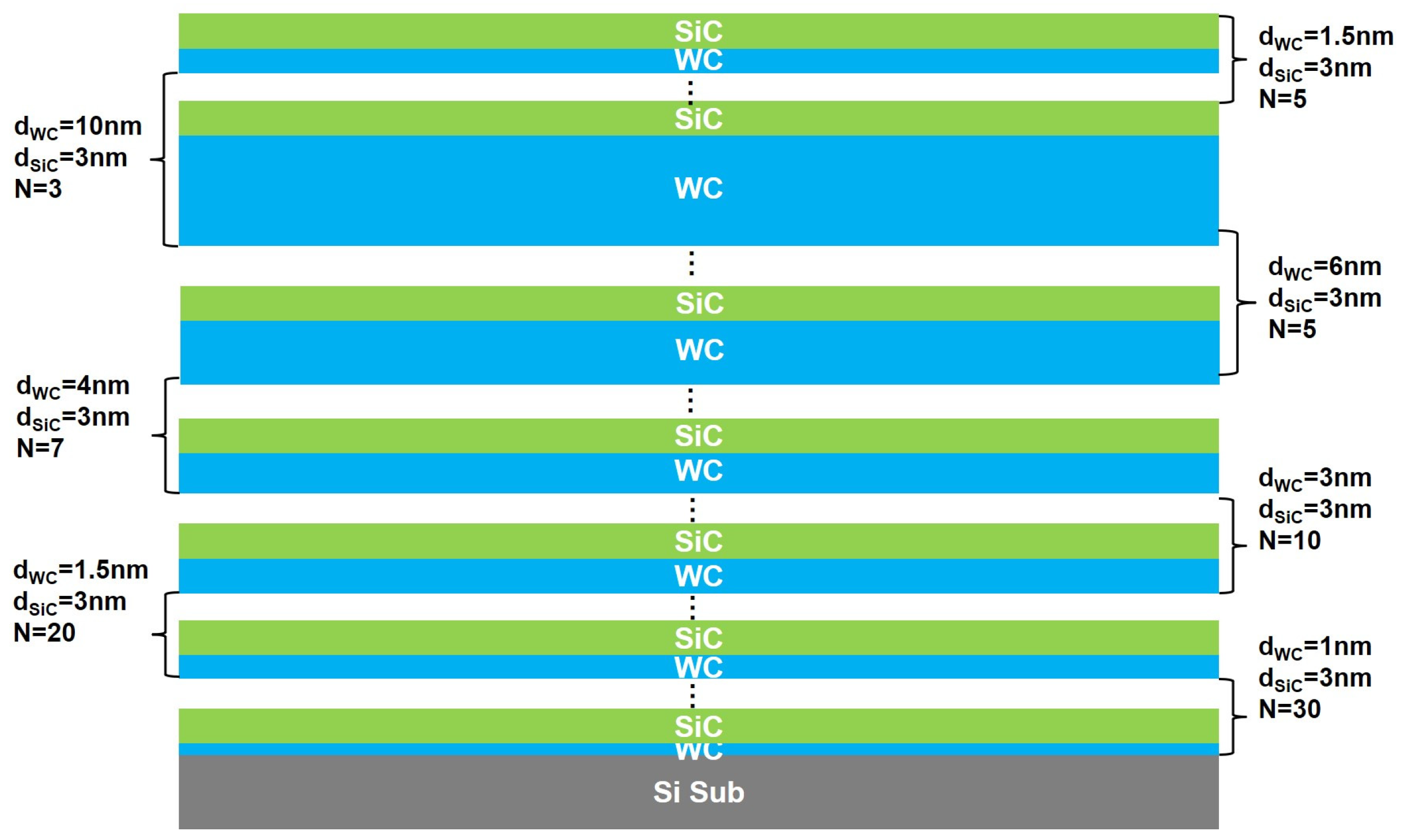
2. Materials and Methods

To investigate the microstructural evolution of the WC layer in WC/SiC multilayers, several periodic WC/SiC multilayers were designed with varied WC thicknesses and a constant SiC thickness. The designed structure parameter of these multilayers is shown in Table 1 (S1, S2, S3, S4, and S5 represent the different samples in the following). The WC layer thickness was changed from 1 nm to 10 nm, while the SiC layer thickness was maintained at 3 nm. The different bilayer numbers ensured that the total WC layer thickness was equal among the different samples. In addition, an aperiodic multilayer was designed to contain varied WC layer thicknesses (mentioned for periodic multilayers) for the convenience of electron microscope analysis. An additional stack with a WC layer thickness of 4 nm was added to this aperiodic multilayer. A schematic of the aperiodic multilayer is shown in Figure 1. The WC/SiC multilayers were fabricated by the direct current magnetron sputtering technique with a planetary rotation system [26], and a schematic of this system is shown in Figure 2. The diameters of the WC (purity: 99.5%) and SiC (purity: 99.5%) targets were both four inches in diameter with a thickness of a quarter of one inch. The constant powers during the deposition of the WC and SiC targets were 20 W and 60 W, respectively. The multilayers were deposited on super-polished commercial Si (100) wafers (20 mm × 20 mm) with a root mean square (RMS) roughness lower than 0.2 nm (1 × 1 μm2 atomic force microscope scan). High-purity argon (99.999%) was used as the working gas at a pressure of 0.16 Pa to maintain the relatively high kinetic energy of the deposited atoms and thus ensure smooth interfaces formed. The substrate was mounted facing downward on a plate that was self-spun as it rotated over each magnetron sputtering source. The self-spinning motion (at a speed of 20 rpm) of the substrate was used to enhance the lateral uniformity of the coating. The individual layer thicknesses in the multilayer were adjusted by independently controlling the residence time of the substrates over each target. The background pressure was lower than 5 × 10⁻⁵ Pa before Ar was inflated.
The grazing incidence X-ray reflectivity (GIXR) measurement was performed with a commercial X-ray diffractometer (Bruker D8 Discover, Billerica, MA, USA) with the Cu Kα line as the source (λ = 0.154 nm). The grazing angle scan range was between 0° and 7°, and the step size was 0.005°. Fitting of GIXR curves was obtained using the Bede Refs software package [27]. The information on the individual layer thickness and average interface width was determined from the fitting. To study the change in the crystallization of multilayers with different WC layer thicknesses, a reference sample was fabricated by DC magnetron sputtering. This sample featured a single WC coating (S0) with a thickness of 120 nm. All the multilayers and WC coatings were characterized at the Shanghai Institute of Silicate using another commercial X-ray diffractometer (Bruker D8 Advance). The X-ray diffraction (XRD) patterns were measured in the symmetrical reflection mode with the Cu Kα line as the source (λ = 0.154 nm). The surface morphology of each sample was characterized by atomic force microscopy (AFM, Bruker Dimension Icon system) in a tapping mode. The scanning region was 1 μm × 1 μm and the scanning area consisted of 256 × 256 pixels.
High-resolution transmission electron microscopy (TEM) measurements were performed to compare the microstructure and layer morphology of the aperiodic WC/SiC multilayer. The test sample was prepared by a focused ion beam and observed with a FEI Talos F200X microscope (Thermo Fisher, Waltham, MA, USA). The elemental compositions of the layers were further measured by energy-dispersive X-ray spectroscopy (EDX) during TEM measurements. One-dimensional line scans across several bilayers were performed to measure the composition depth profiles of different elements.

3. Results and Discussion

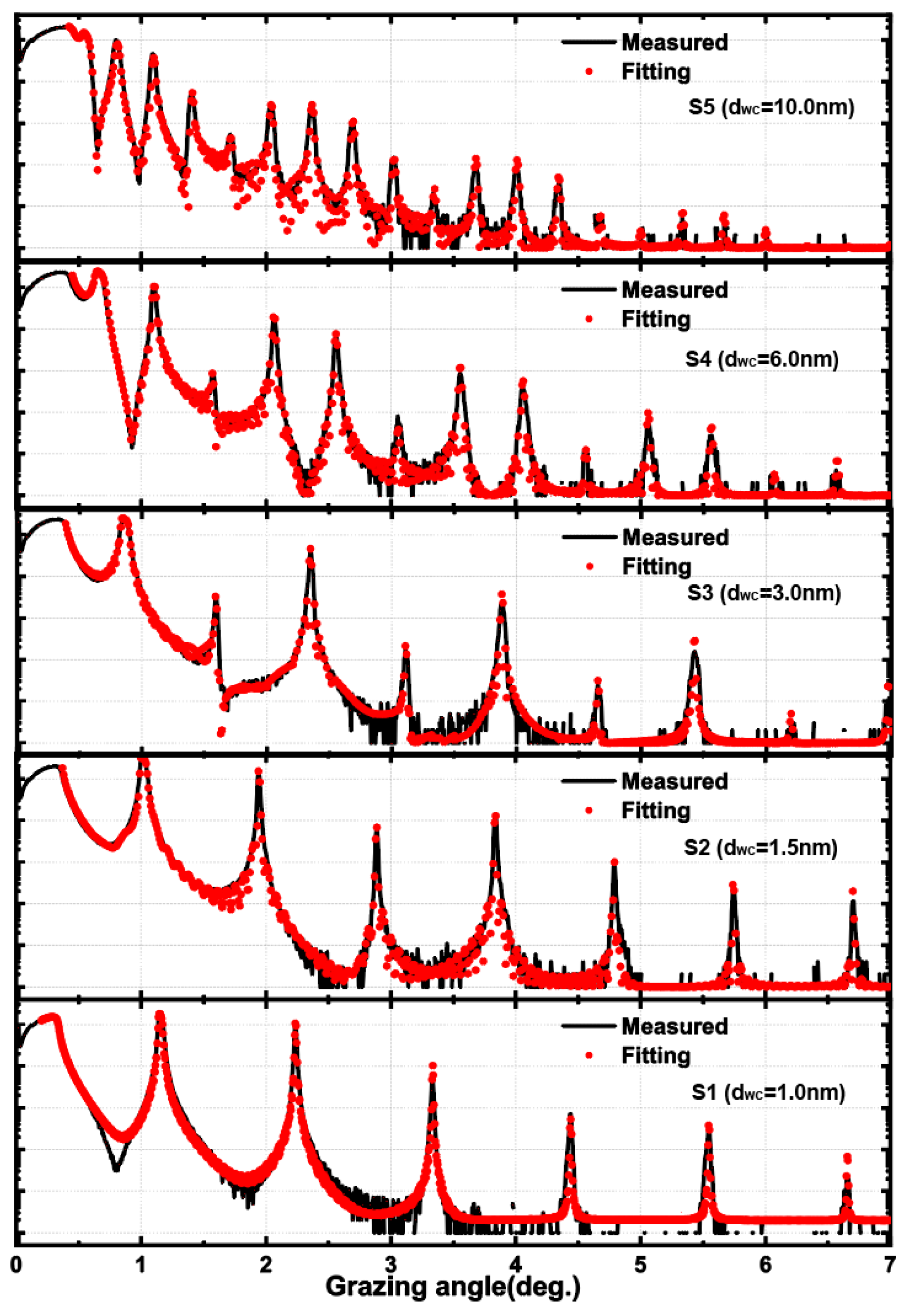
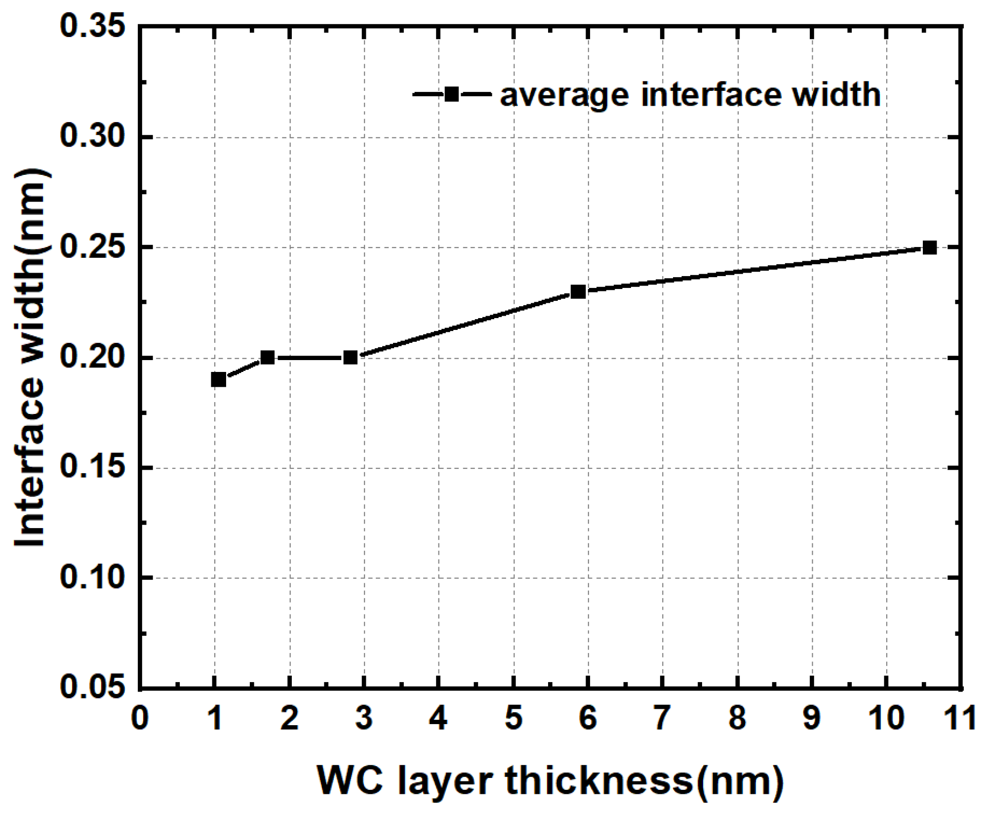
3.1. GIXR Measurement Analysis

Figure 3 shows the GIXR measurement curves and fitted results for the periodic WC/SiC multilayers. The optical constants of WC and SiC were obtained from the website of the Center for X-ray Optics [28]. From the bottom to the top, the thickness of the WC layer varied from 1.0 nm to 10 nm. The fitted results matched very well with the GIXR measurements, both for the bandwidth and peak values. The layer thickness and average interface width were fitted using a genetic algorithm and the fitted parameters are listed in Table 2 [29]. The fitted parameters of the fabricated multilayers had a little bit of deviation from the designed structures, which could have been caused by a small error in the deposition rate calibration. In the data fitting work, the densities of silicon carbide and tungsten carbide are close to the bulk material density (WC: 15.63 g/cm3; SiC: 3.21 g/cm3). As the WC layer thickness increased, the average interface width also increased. From samples S1 to S3, the interface width only slightly changed from 0.19 nm to 0.20 nm. However, from S3 to S5, the average interface width increased significantly, as shown in Figure 4. Based on previous research, we can assume that the microstructure of the WC layer changes as the layer thickness increases, which contributes to an increase in the average interface width [25]. Further analysis is required to investigate the changes that occur in WC/SiC multilayers.

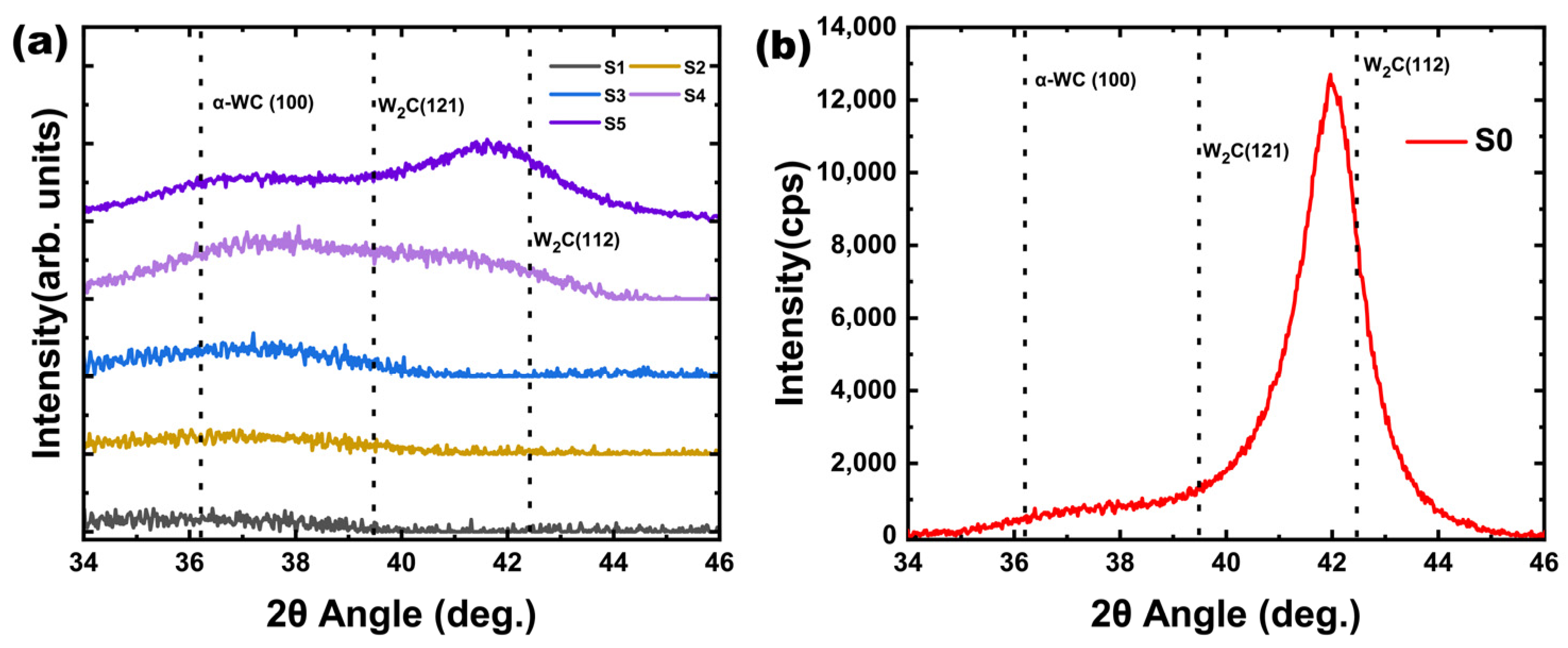
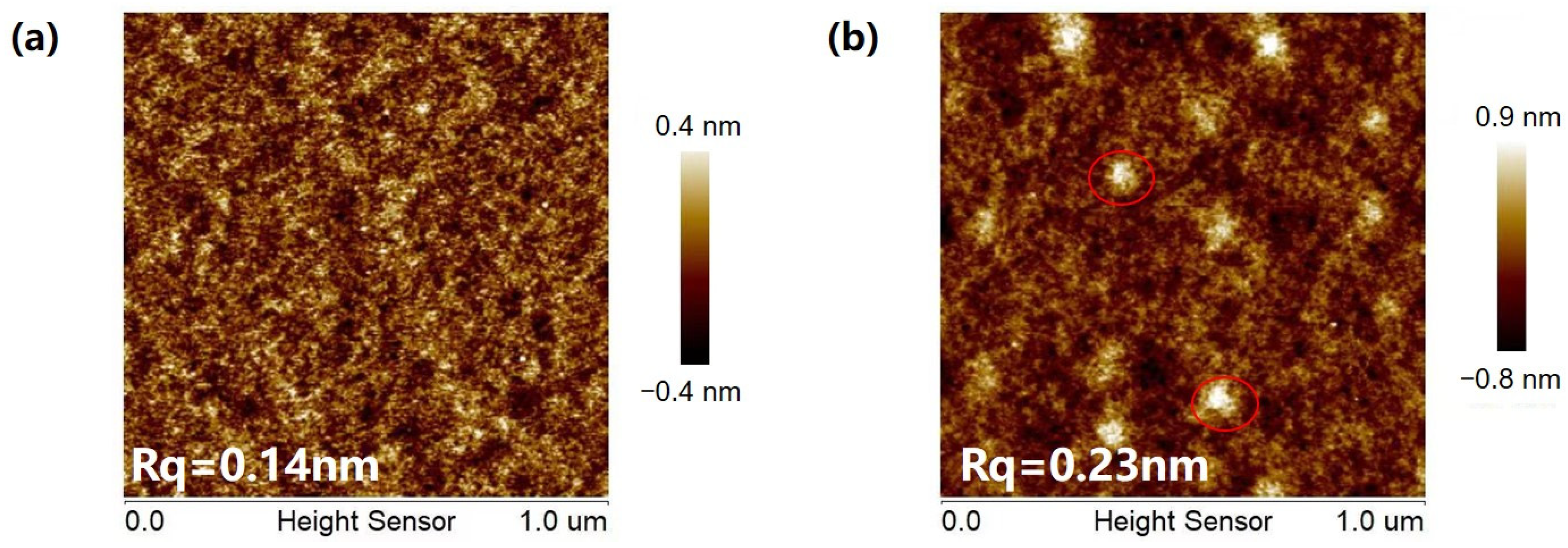
3.2. XRD and AFM Measurement Analysis

Figure 5a shows the measured XRD patterns of the WC/SiC multilayers with different WC layer thicknesses. As the WC layer thickness increases from 1.0 nm to 3.0 nm, the intensity of the broad bump between 34° and 40° gradually increases. As the WC layer thickness increased to around 10.0 nm, another broad peak between 40° and 42° appeared. To further confirm that the signal originated from the WC layer, a single-layer WC coating (S0) was tested under the same conditions. As shown in Figure 5b, there was an obvious peak at 42°, which meant the WC coating was strongly crystallized. The three dashed lines in Figure 5 represent the 2θ positions of α-WC (100), W2C (121), and W2C (112). These positions were determined according to the powder diffraction files (PDFs) from the International Centre for Diffraction Data (ICDD): α-WC (PDF 51-0939) [30] and W2C (PDF 89-2371) [31].
Based on the XRD measurements, we found that the increase in average interface width coincided with the enhancement in crystallization in the WC/SiC multilayer. As the WC layer reached approximately 6.0 nm (S4), the intensity of the XRD patterns at 37° increased significantly compared to the thinner samples (S1–S3). This could have been due to the change of the WC layer from the quasi-amorphous to the crystalline phase. The orientation of the WC grains appeared close to α-WC (100). Nanograin formation led to an abrupt change in the average interface width. As the WC layer became thicker (S5), the crystalline state of the WC layer showed a preference for W2C.
To investigate the change in the morphology for the WC/SiC multilayer from an amorphous to a crystallized state, S1 and S5 were tested by AFM over an area of 1 μm × 1 μm. Figure 6 presents surface images of samples S1 and S5. The surface of S1 was smooth with a root mean square (RMS) roughness of 0.14 nm. As the WC layer increased to 10.0 nm, the RMS roughness increased to 0.23 nm. Some crystallized features (broad bumps with an average size of about 85 nm, marked in red circles) are shown in Figure 6b, which is similar to the phenomena mentioned in other studies [32,33]. The changes in the surface morphology and surface roughness were consistent with the GIXR and XRD results.

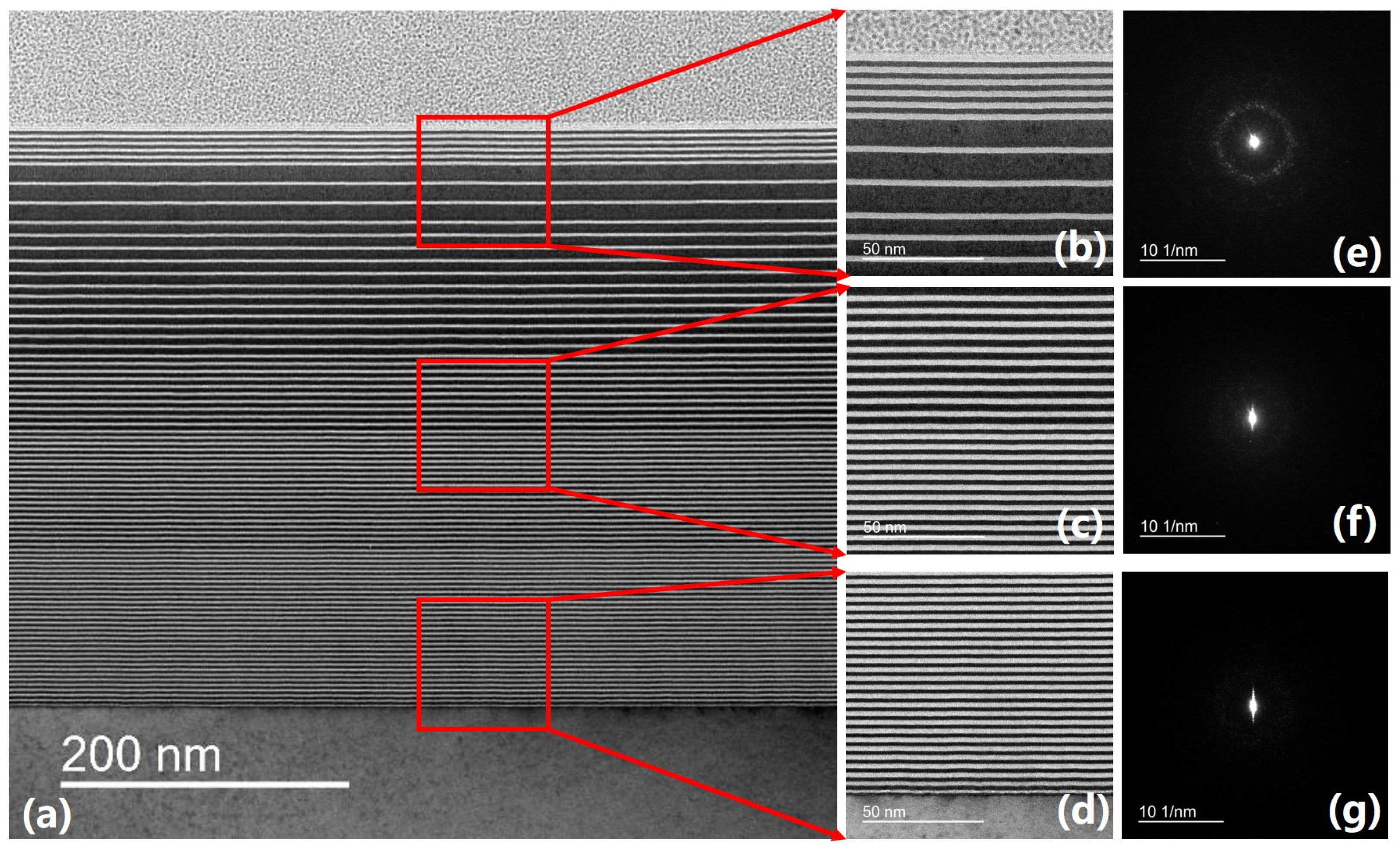
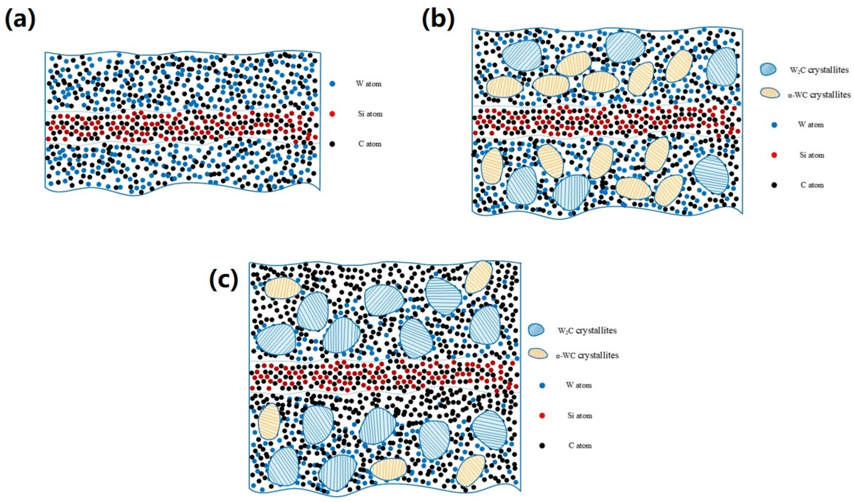
3.3. Transmission Electron Microscope Analysis

The cross-sectional TEM images and selected area electron diffraction (SAED) patterns of the aperiodic WC/SiC multilayer are shown in Figure 7. The bright layers are SiC and the dark layers are WC. Figure 7a shows a full view of the aperiodic sample. From the full view, the thickness of the individual layer is close to the designed value (shown in Figure 1). Figure 7b–d show enlarged views of different positions (red squares in Figure 7a) of this sample. In Figure 7b, the broadest dark layer is the WC layer with a thickness of 10.0 nm. Figure 7c shows the middle part of this aperiodic multilayer, where the WC layers thicknesses shown are 3.0 nm and 1.5 nm. Figure 7d is close to the substrate and only contains the WC layer with a thickness of 1.0 nm. From these images, we found that all the layers were flat, and the diffusion between adjacent layers was negligible. At the bottom of this sample, the small d-spacing part showed good uniformity. At the top part, there were some darker spots in the WC layer, which may have been due to the WC grains shown in the XRD measurements.
SAED images were recorded with an electron beam with a diameter smaller than 20.0 nm. Such a small beam could help with evaluating the crystallization of the WC layer with a certain thickness in this sample. The corresponding SAED images in Figure 7b–d are shown in Figure 7e–g. Only Figure 7f,g show a diffraction pattern that originated from the multilayer structure, which indicated an amorphous and uniform layer structure in these parts. However, the diffraction pattern shown in Figure 7e has a faint and broad ring when compared with the other two images, indicating the layer structure was not amorphous. We performed a SAED test on each stack with different WC layer thicknesses (only three results are shown in this work), and the faint ring shown in Figure 7e first appeared when the WC thickness reached 6.0 nm. As the WC thickness increased from 6.0 nm to 10.0 nm, this faint ring became brighter, which meant the crystallization in the WC layer became stronger. The faint ring could have resulted from the W2C grain formed in the WC layer, which is consistent with the XRD results.

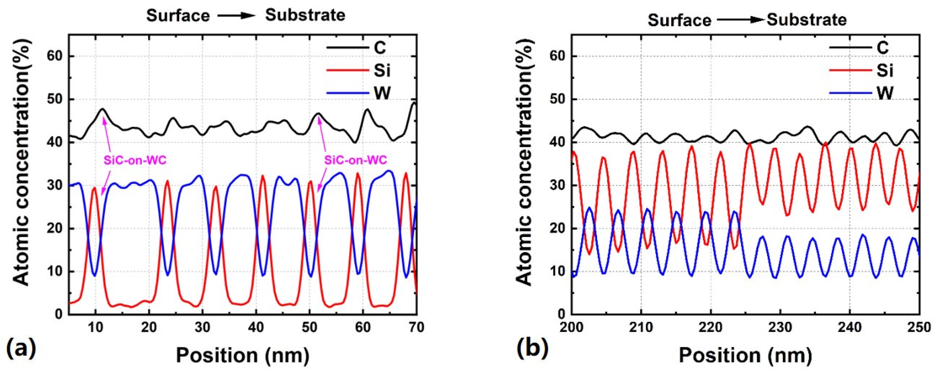
3.4. Energy-Dispersive X-ray Spectroscopy Analysis

Based on previous research, for a multilayer that contained a crystalline layer, it was hard to control the value of the average interface width to be smaller than 0.3 nm. Especially when the thickness of the crystallized layer reached 10.0 nm, the average interface width was larger than 0.5 nm. In our work, although the average interface width of the WC/SiC multilayer increased as the crystallization in the WC layer became stronger, the value was still smaller than 0.3 nm. For further analysis of how the WC/SiC multilayer maintains the average interface width, EDX one-dimensional line scans across several bilayers were performed during the TEM measurement.
The EDX measurement allowed us to determine the atomic concentrations of different elements in the aperiodic WC/SiC multilayer sample. In this study, the EDX measurements were performed to characterize tungsten (W), carbon (C), and silicon (Si). The detailed one-dimensional line scans at different positions of the aperiodic sample are shown in Figure 8a,b. Figure 8a shows the data close to the surface, which contained a 10.0 nm and 6.0 nm WC layer stack. Figure 8b shows the data close to the substrate, which contained a thinner WC layer stack (1.5 nm and 1.0 nm). All the measured elements had a periodic oscillation of concentration, as shown in Figure 8a,b, which further illustrates that the aperiodic sample had a uniform layer structure. However, for the carbon atomic concentration curves, there was an accumulation that appeared at the SiC-on-WC interface when the SiC was deposited on a thicker WC layer (≥6.0 nm). In the thinner stack, the oscillation of the C atomic concentration was smaller than 5%, whereas in the thicker stack, this oscillation was close to 10%.
Based on the comprehensive measurements and analysis presented in this section, we formulated a plausible model for the evolution of the physical characteristics in WC/SiC multilayer films, as shown in Figure 9. When the WC layer was relatively thin, both the WC and SiC layers were amorphous. The C atoms were almost uniformly located in the entire multilayer, reducing the diffusion between W and Si atoms [12]. Therefore, the interface width was very small in the thinner stack. As the thickness of the WC layer increased, WC grains began to emerge. Initially, these grains mostly manifested as α-WC grains. As the WC layer continued to thicken, there was a noticeable change in the crystalline state, transitioning from α-WC to W2C. Simultaneously, dissociative C atoms were pushed by the emerging tiny grains within the WC layer, migrating toward the SiC-on-WC interface. These C atoms helped smooth the crystalline WC layer, ensuring that the interface width did not escalate significantly. Thus, even as the WC layer evolves, the WC/SiC combination maintains excellent interfacial properties.

4. Conclusions

The experimental findings offer a detailed insight into the WC layer evolution mechanisms within WC/SiC multilayers. We also constructed a model to account for the migration of carbon atoms toward the WC/SiC interface. Utilizing measurements from GIXR, XRD, AFM, and TEM, it was confirmed that the carbon atom distribution was almost uniformly within the entire multilayer when the WC layer was thin. As the WC layer thickness increased, the carbon atoms began to move towards the SiC-on-WC interface.
When the WC layer thickness was within the range of 1.0 nm to 3.0 nm, the layer was amorphous. As the thickness of the WC layer increased, minimal grains emerged in the WC layer in the form of an α-WC (100) orientation. As the thickness further increased, the orientation transformed to W2C (121) and W2C (112), and the crystallinity became stronger. The enhanced crystallinity in the WC layer caused carbon atoms to migrate toward the SiC-on-WC interface. This migration not only inhibited the interaction of tungsten and silicon at the interface but also mitigated the impact of the W2C grains on the interface quality.
However, it is crucial to note that in this study, the thickness of the SiC layer in the test samples was kept constant to specifically assess the impact of the WC layer’s thickness on the overall multilayer system. The effects of variations in the SiC layer thickness on the system remain an open question and will be the focus of future research.

Author Contributions

Conceptualization, Z.Z. (Zhe Zhang), Z.Z. (Zhong Zhang) and Z.W. (Zhanshan Wang); methodology, T.L. and Z.W. (Zile Wang); software, T.L., Q.H. and R.Q.; validation, Z.Z. (Zhe Zhang) and Z.W. (Zhanshan Wang); formal analysis, L.J. and Z.Z. (Zhe Zhang); investigation, Z.Z. (Zhe Zhang); resources, R.Q.; data curation, L.J. and Q.H.; writing—original draft preparation, T.L. and Z.Z. (Zhe Zhang); writing—review and editing, Z.Z. (Zhong Zhang) and Z.W. (Zhanshan Wang); visualization, T.L.; supervision, Z.Z. (Zhe Zhang) and Z.Z. (Zhong Zhang); project administration, Z.Z. (Zhong Zhang) and Z.W. (Zhanshan Wang); funding acquisition, Z.Z. (Zhe Zhang) and Z.Z. (Zhong Zhang). All authors have read and agreed to the published version of the manuscript.

Funding

This research was funded by the National Key Research and Development Program of China (2022YFF0709100) and the National Natural Science Foundation of China [grant No. 12204353].

Institutional Review Board Statement

Not applicable.

Informed Consent Statement

Not applicable.

Data Availability Statement

The data presented in this study are available on request from the corresponding author.

Conflicts of Interest

The authors declare no conflicts of interest.

References

  1. Lider, V.V. Multilayer X-ray Interference Structures. Uspekhi Fiz. Nauk 2019, 189, 1137–1171. [Google Scholar] [CrossRef]
  2. Spiller, E. 14. Reflecting Optics: Multilayers. In Vacuum Ultraviolet Spectroscopy I; Lucatorto, T., Samson, J.A., Ederer, D.L., De Graef, M., Eds.; Academic Press: Cambridge, MA, USA, 1998; Volume 31, pp. 271–288. ISBN 1079-4042. [Google Scholar]
  3. Huang, Q.; Medvedev, V.; Van de Kruijs, R.; Yakshin, A.; Louis, E.; Bijkerk, F. Spectral Tailoring of Nanoscale EUV and Soft X-ray Multilayer Optics. Appl. Phys. Rev. 2017, 4, 011104. [Google Scholar] [CrossRef]
  4. Barrett, R.; Baker, R.; Cloetens, P.; Morawe, C.; Tucoulou, R.; Vivo, A. Reflective Optics for Hard X-ray Nanofocusing Applications at the ESRF. Synchrotron Radiat. News 2016, 29, 10–15. [Google Scholar] [CrossRef]
  5. Windt, D.L. Advancements in Hard X-ray Multilayers for X-ray Astronomy. In Optics for EUV, X-ray, and Gamma-ray Astronomy VII, Proceedings of the SPIE Optical Engineering + Applications 2005, San Diego, CA, USA, 9–13 August 2015; SPIE: Bellingham, WA, USA, 2015; Volume 9603, p. 96031C. [Google Scholar] [CrossRef]
  6. Leake, S.J.; Chahine, G.A.; Djazouli, H.; Zhou, T.; Richter, C.; Hilhorst, J.; Petit, L.; Richard, M.I.; Morawe, C.; Barrett, R.; et al. The Nanodiffraction Beamline ID01/ESRF: A Microscope for Imaging Strain and Structure. J. Synchrotron Radiat. 2019, 26, 571–584. [Google Scholar] [CrossRef]
  7. Pradhan, P.C.; Gangir, D.; Majhi, A.; Nayak, M.; Biswas, A.; Bhattacharyya, D.; Lodha, G.S. Fabrication and Performance of a High Resolution Ultra-Short Period W/B4C Multilayer Structure. J. Phys. D Appl. Phys. 2016, 49, 135305. [Google Scholar] [CrossRef]
  8. Majhi, A.; Nayak, M.; Pradhan, P.C.; Jena, S.; Gome, A.; Singh, M.N.; Srivastava, H.; Reddy, V.R.; Srivastava, A.K.; Sinha, A.K.; et al. Sub-Nanograin Metal Based High Efficiency Multilayer Reflective Optics for High Energies. RSC Adv. 2021, 11, 28097–28105. [Google Scholar] [CrossRef]
  9. Chon, K.S. Trilayer Model in Design of W/C Multilayer Mirrors with a Small Period Thickness. J. Mech. Sci. Technol. 2019, 33, 5837–5842. [Google Scholar] [CrossRef]
  10. Christensen, F.E.; Jensen, C.P.; Madsen, K.K.; Pivovaroff, M.J.; Chen, H.; Dariel, A.; Høghøj, P. Novel Multilayer Designs for Future Hard X-ray Missions. In Space Telescopes and Instrumentation II: Ultraviolet to Gamma Ray, Proceedings of the SPIE Astronomical Telescopes + Instrumentation 2006, Orlando, FL, USA, 24–31 May 2006; Society of Photo-Optical Instrumentation Engineers: Bellingham, WA, USA, 2006; Volume 6266, p. 626611. [Google Scholar] [CrossRef]
  11. Louis, E.; Yakshin, A.E.; Tsarfati, T.; Bijkerk, F. Nanometer Interface and Materials Control for Multilayer EUV-Optical Applications. Prog. Surf. Sci. 2011, 86, 255–294. [Google Scholar] [CrossRef]
  12. Yang, Z.; Zhu, J.; Zhu, Y.; Luo, H.; Li, Z.; Jiang, H.; Zhao, L. Asymmetric Interface and Growth Mechanism in Sputtered W/Si and WSi2/Si Multilayers. Appl. Surf. Sci. 2022, 604, 154531. [Google Scholar] [CrossRef]
  13. Harrison, F.A.; Boggs, S.E.; Bolotnikov, A.E.; Christensen, F.E.; Cook, W.R., III; Craig, W.W.; Hailey, C.J.; Jimenez-Garate, M.A.; Mao, P.H.; Schindler, S.M.; et al. Development of the High-Energy Focusing Telescope (HEFT) Balloon Experiment. In X-ray Optics, Instruments, and Missions III, Proceedings of the Astronomical Telescopes and Instrumentation 2000, Munich, Germany, 17–31 March 2000; Truemper, J.E., Aschenbach, B., Eds.; SPIE: Bellingham, WA, USA, 2000; Volume 4012, pp. 693–699. [Google Scholar]
  14. Jensen, C.P.; Madsen, K.K.; Christensen, F.E. Small D-Spacing WC/SiC Multilayers for Future Hard X-ray Telescope Designs. Exp. Astron. 2005, 20, 93–103. [Google Scholar] [CrossRef]
  15. Jensen, C.P.; Madsen, K.K.; Christensen, F.E. Investigation of New Material Combinations for Hard X-ray Telescope Designs. In Space Telescopes and Instrumentation II: Ultraviolet to Gamma R, Proceedings of the SPIE Astronomical Telescopes + Instrumentation 2006, Orlando, FL, USA, 24–31 May 2006; SPIE: Bellingham, WA, USA, 2006; Volume 6266, p. 626612. [Google Scholar] [CrossRef]
  16. Larruquert, J.I. Optical Properties of Thin Film Materials at Short Wavelengths; Elsevier: Amsterdam, The Netherlands, 2018; ISBN 9780081020739. [Google Scholar]
  17. Fernández-Perea, M.; Pivovaroff, M.J.; Soufli, R.; Alameda, J.; Mirkarimi, P.; Descalle, M.A.; Baker, S.L.; McCarville, T.; Ziock, K.; Hornback, D.; et al. Ultra-Short-Period WC/SiC Multilayer Coatings for X-ray Applications. Nucl. Instrum. Methods Phys. Res. Sect. A Accel. Spectrometers Detect. Assoc. Equip. 2013, 710, 114–119. [Google Scholar] [CrossRef]
  18. Fernández-Perea, M.; Descalle, M.A.; Soufli, R.; Ziock, K.P.; Alameda, J.; Baker, S.L.; McCarville, T.J.; Honkimäki, V.; Ziegler, E.; Jakobsen, A.C.; et al. Physics of Reflective Optics for the Soft Gamma-Ray Photon Energy Range. Phys. Rev. Lett. 2013, 111, 1–5. [Google Scholar] [CrossRef]
  19. Pivovaroff, M.J.; Ziock, K.P.; Fernandez-Perea, M.; Harrison, M.J.; Soufli, R. Gamma-Ray Mirrors for Direct Measurement of Spent Nuclear Fuel. Nucl. Instrum. Methods Phys. Res. Sect. A Accel. Spectrometers Detect. Assoc. Equip. 2014, 743, 109–113. [Google Scholar] [CrossRef]
  20. Brejnholt, N.F.; Decker, T.A.; Hill, R.M.; Chen, H.; Williams, G.J.; Park, J.; Alameda, J.B.; Fernández-Perea, M.; Pivovaroff, M.J.; Soufli, R.; et al. Reflective Multilayer Optic as Hard X-ray Diagnostic on Laser-Plasma Experiment. Rev. Sci. Instrum. 2015, 86, 013110. [Google Scholar] [CrossRef]
  21. Bajt, S.; Prasciolu, M.; Fleckenstein, H.; Domaracký, M.; Chapman, H.N.; Morgan, A.J.; Yefanov, O.; Messerschmidt, M.; Du, Y.; Murray, K.T.; et al. X-ray Focusing with Efficient High-NA Multilayer Laue Lenses. Light Sci. Appl. 2018, 7, 17162. [Google Scholar] [CrossRef]
  22. Prasciolu, M.; Bajt, S. On the Properties of WC/SiC Multilayers. Appl. Sci. 2018, 8, 571. [Google Scholar] [CrossRef]
  23. Zhang, Q.; Zhang, Z.; Liu, Y.; Wang, Z. Crystallization and Composition of Ni-C/Ti Multilayer with Varied Ni-C Thickness. Coatings 2022, 12, 1144. [Google Scholar] [CrossRef]
  24. Zhong, Q.; Zhang, Z.; Ma, S.; Qi, R.; Li, J.; Wang, Z.; Le Guen, K.; André, J.M.; Jonnard, P. The Transition from Amorphous to Crystalline in Al/Zr Multilayers. J. Appl. Phys. 2013, 113, 133508. [Google Scholar] [CrossRef]
  25. Feng, Y.; Zhang, Z.; Qi, R.; Huang, Q.; Wang, Z. Microstructural Evolution of Ni/Ti Multilayers Doped with Nitrogen at Different d-Spacings for Neutron Supermirrors. Vacuum 2023, 210, 111881. [Google Scholar] [CrossRef]
  26. Oliver, J.B. Analysis of a Planetary-Rotation System for Evaporated Optical Coatings. Appl. Opt. 2016, 55, 8550. [Google Scholar] [CrossRef]
  27. Wei, Z.; Zhang, Z.; Jiang, L.; Yang, Y.; Chang, C.; Feng, Y.; Qi, R.; Huang, Q.; Yan, W.; Xie, C.; et al. Background Pressure Induced Structural and Chemical Change in NiV/B4C Multilayers Prepared by Magnetron Sputtering. Front. Phys. 2022, 10, 837819. [Google Scholar] [CrossRef]
  28. Henke, B.L.; Gullikson, E.M.; Davis, J.C. X-ray Interactions: Photoabsorption, Scattering, Transmission, and Reflection at E = 50–30,000 EV, Z = 1–92. At. Data Nucl. Data Tables 1993, 54, 181–342. [Google Scholar] [CrossRef]
  29. Wormington, M.; Panaccione, C.; Matney, K.M.; Bowen, D.K. Characterization of Structures from X-ray Scattering Data Using Genetic Algorithms. Philos. Trans. R. Soc. Lond. Ser. A Math. Phys. Eng. Sci. 1999, 357, 2827–2848. [Google Scholar] [CrossRef]
  30. Smetanina, K.E.; Andreev, P.V.; Lantsev, E.A.; Nokhrin, A.V.; Murashov, A.A.; Isaeva, N.V.; Blagoveshchensky, Y.V.; Boldin, M.S.; Chuvil’deev, V.N. Nonuniform Distribution of Crystalline Phases and Grain Sizes in the Surface Layers of WC Ceramics Produced by Spark Plasma Sintering. Coatings 2023, 13, 1051. [Google Scholar] [CrossRef]
  31. Wang, Y.; Chen, J.; Gong, L.; Tang, J.; Wang, X.; Guo, H.; Zhou, X. P-Doped W2C Nanoparticles for Hydrogen Evolution Reaction Powered by a Wind-Driven Triboelectric Nanogenerator. Nano Energy 2024, 121, 109242. [Google Scholar] [CrossRef]
  32. Mazur, M.; Poniedziałek, A.; Kaczmarek, D.; Wojcieszak, D.; Domaradzki, J.; Gibson, D. Investigation of Various Properties of HfO2-TiO2 Thin Film Composites Deposited by Multi-Magnetron Sputtering System. Appl. Surf. Sci. 2017, 421, 170–178. [Google Scholar] [CrossRef]
  33. Obstarczyk, A.; Kaczmarek, D.; Wojcieszak, D.; Mazur, M.; Domaradzki, J.; Kotwica, T.; Pastuszek, R.; Schmeisser, D.; Mazur, P.; Kot, M. Tailoring Optical and Electrical Properties of Thin-Film Coatings Based on Mixed Hf and Ti Oxides for Optoelectronic Application. Mater. Des. 2019, 175, 107822. [Google Scholar] [CrossRef]
Figure 1. Schematic of the aperiodic WC/SiC multilayer for TEM measurement.
Coatings 14 00720 g001
Figure 2. Schematic of the magnetron sputtering system.
Coatings 14 00720 g002
Figure 3. GIXR measurement (black lines) and fitted (red dots) curves of periodic WC/SiC multilayers with varied WC layer thicknesses.
Coatings 14 00720 g003
Figure 4. Average interface width as a function of the WC layer thickness.
Coatings 14 00720 g004
Figure 5. Measured XRD patterns: (a) WC/SiC multilayers with varied WC layer thicknesses; (b) WC coating.
Coatings 14 00720 g005
Figure 6. AFM measurement of WC/SiC multilayer with different WC layer thicknesses: (a) WC = 1.0 nm; (b) WC = 10.0 nm.
Coatings 14 00720 g006
Figure 7. Transmission electron microscopy (TEM) and selected area electron diffraction (SAED) images of the aperiodic WC/SiC multilayers: (a) magnification: 36,000×; (bd) magnification: 190,000×; (eg) SAED pattern.
Coatings 14 00720 g007
Figure 8. EDX line scan (from surface to substrate) measurements of chemical elements in aperiodic WC/SiC multilayer: (a) scan area close to surface; (b) scan area close to substrate.
Coatings 14 00720 g008
Figure 9. The microstructure evolution model of WC/SiC multilayer as WC layer thickness increased: (a) amorphous state; (b) crystalline state emerged (mainly manifests as α-WC); (c) crystalline state enhanced (mainly manifested as W2C).
Coatings 14 00720 g009
Table 1. The design structure of periodic WC/SiC multilayers.
S1S2S3S4S5
WC thickness (dWC)1 nm1.5 nm3 nm6 nm10 nm
SiC thickness (dSiC)3 nm3 nm3 nm3 nm3 nm
Period4 nm4.5 nm6 nm9 nm13 nm
Number of bilayers (N)12080402012
Residence time for WC12.72 s19.08 s38.16 s76.32 s127.20 s
Table 2. The fitted parameters of periodic WC/SiC multilayers.
S1S2S3S4S5
WC thickness (dWC)1.05 nm1.71 nm2.82 nm5.87 nm10.58 nm
SiC thickness (dSiC)2.94 nm2.91 nm2.90 nm2.90 nm2.73 nm
Average interface width0.19 nm0.20 nm0.20 nm0.23 nm0.25 nm
Number of bilayers (N)12080402012
Disclaimer/Publisher’s Note: The statements, opinions and data contained in all publications are solely those of the individual author(s) and contributor(s) and not of MDPI and/or the editor(s). MDPI and/or the editor(s) disclaim responsibility for any injury to people or property resulting from any ideas, methods, instructions or products referred to in the content.

