Article

Preparation of Highly Efficient and Stable All-Inorganic CsPbBr3 Perovskite Solar Cells Using Pre-Crystallization Multi-Step Spin-Coating Method

1
Department of Basic Courses, Officers College of PAP, Chengdu 610213, China
2
School of Applied Science, Taiyuan University of Science and Technology, Taiyuan 610213, China
3
Hangzhou Acme Optoelectronics Technology Co., Ltd., Hangzhou 310020, China
4
Center of Condensed Matter and Material Physics, School of Physics, Beihang University, Beijing 100191, China
*
Authors to whom correspondence should be addressed.
These authors contributed equally to this work.
Coatings 2024, 14(7), 918; https://doi.org/10.3390/coatings14070918 (registering DOI)
Submission received: 3 July 2024 / Revised: 19 July 2024 / Accepted: 20 July 2024 / Published: 22 July 2024

Abstract

:
All-inorganic CsPbBr3 perovskite solar cells have garnered extensive attention in the photovoltaic domain due to their remarkable environmental stability. Nevertheless, CsPbBr3 prepared using the conventional sequential deposition method suffers from issues such as inferior crystallinity, low phase purity, and poor film morphology. Herein, we propose a pre-crystallization methodology by introducing a minute quantity of CsBr into the PbBr2 precursor solution to generate a small amount of CsPb2Br5 crystals within the PbBr2 film, leading to a porous PbBr2 film with enhanced crystallinity. Under the influence of more pores and CsPb2Br5 crystals as nucleation sites for inducing growth, a CsPbBr3 film with a larger crystal size, lower grain boundary density, stronger crystallinity, and higher phase purity is formed. Compared with untreated devices, photovoltaic devices prepared using the pre-crystallization method achieved a champion photovoltaic conversion efficiency (PCE) of 8.62%. Furthermore, pre-crystallized devices demonstrate higher stability than untreated ones and can still retain 94% of the original PCE after being exposed to air for 1000 h without encapsulating.

1. Introduction

Organic–inorganic hybrid perovskite possesses outstanding photovoltaic performance, rendering it the most popular photovoltaic material in recent years. Ever since its initial preparation in 2009, the power conversion efficiency (PCE) of organic–inorganic hybrid perovskite solar cells (PSCs) has witnessed a remarkable increase from 3.8% to the current maximum of 26.41% [1,2,3,4]. Nevertheless, on account of the hydrophobic nature and instability of organic cations (MA+ and FA+), organic–inorganic hybrid perovskites demonstrate chemical instability when exposed to harsh environments such as humidity, high temperature, light, and oxygen, thereby restricting the long-term stability of PSCs [5,6]. The method of using Cs+ ions in lieu of organic cations to enhance stability and thermal stability has been verified as feasible [7]. Among them, CsPbI3 PSC has attained the highest PCE of 21.86% [8]. However, CsPbI3 perovskite demands a high temperature to sustain its ideal black cubic α phase, and it readily undergoes a transformation into the yellow orthorhombic δ-non-perovskite phase at room temperature and in moist environments, boasting unfavorable photoelectric properties [9]. The employment of Br as a halide anion leads to a more stable black phase at room temperature, thanks to the enhanced effective tolerance factor and lower phase-transition temperature [10]. In comparison to CsPbI2Br and CsPbIBr2, CsPbBr3 perovskites that completely substitute I with Br enjoy the most robust environmental stability [11,12,13]. Nevertheless, the light-absorption capacity of CsPbBr3 is compromised by its wider bandgap, posing a challenge to enhancing the efficiency of the single-layer CsPbBr3 PSC [14,15].
Since no suitable solvent exists that exhibits excellent solubility for both PbBr2 and CsBr, CsPbBr3 is typically prepared through a multi-step method. Liang et al. proposed a solvent vapor-phase annealing technique to prepare porous PbBr2 films by utilizing the N,N-dimethylformamide (DMF) gas phase environment during the annealing of PbBr2 films. The porous PbBr2 framework can facilitate a reaction with CsBr, thereby attaining dense, uniform, and high-quality large-grain CsPbBr3 films. Consequently, a higher PCE can be obtained, and the unencapsulated device can still retain over 90% of its original PCE after being placed for 30 days [16]. Cao et al. employed a polymer of polyethylene oxide (PEO) as an additive to the PbBr2 solution, transforming the small-grain CsPbBr3 films into equiaxed large grains with a preferred crystal orientation, significantly enhancing the efficiency of the fabricated carbon hole transport layer (HTL) solar cells [17]. Zhao et al. proposed a two-in-one additive engineering strategy in which 4-tert butylpyridine (TBP) and dimethyl sulfoxide (DMSO) were added as additives to the PbBr2 precursor solution and CsBr solution, respectively. The prepared perovskite layer exhibits better permeability, a lower carrier recombination rate, and high absorption capacity, thereby improving the power conversion efficiency. Moreover, the unencapsulated PSC maintains extremely high stability after being stored in ambient air for 1600 h [18]. Based on the two-step method, Che et al. prepared perovskite films using a total of four steps: spin coating low concentration CsBr solution, PbBr2 solution, CsBr solution, and low concentration PbBr2 solution. A PbBr2 film with fewer pores, enhanced crystallinity, and a smoother surface was obtained, and the introduction of the derivative phase CsPb2Br5 promoted the formation of high-quality CsPbBr3 films with larger grains. This film reduces interface defects, enhances grain growth, significantly improves power conversion efficiency, and can maintain stability for over 2400 h in an air environment [19]. Chi et al. introduced indium tribromide (InBr3) into the precursor solution of PbBr2 to form an InBr3(DMF)3 adduct, thereby accelerating the release of organic molecules in PbBr2(DMF) and preparing a porous PbBr2 film. It not only optimizes the morphology of the CsPbBr3 film but also reduces impurity phases. As a result, InBr3:CsPbBr3 perovskite solar cells achieved an efficiency of 7.28% [20]. In recent research, it can be observed that in the process of preparing CsPbBr3 perovskite films via the multi-step method, optimizing the morphology of PbBr2 films can further enhance the crystal quality of perovskite films, thereby improving the performance and stability of their photovoltaic devices [21,22,23,24].
In this work, the pre-crystallization method we previously explored for the preparation of organic–inorganic hybrid perovskite was adopted for the preparation of all-inorganic CsPbBr3 perovskite solar cells [25]. By introducing a small quantity of CsBr into the precursor solution of PbBr2, a minor amount of CsPb2Br5 crystals emerged in the PbBr2 film, and a porous PbBr2 film with higher crystallinity was acquired. Under the influence of the CsPb2Br5 crystal as the nucleus induction and the porous PbBr2 film, a uniform and pure-phase highly crystalline CsPbBr3 film with large grains was formed. The device with the FTO/SnO2/CsPbBr3/carbon configuration prepared using the pre-crystallization method displayed a champion PCE of 8.62%, a short-circuit current density (Jsc) of 7.96 mA/cm2, an open-circuit voltage (Voc) of 1.351 V, as well as a fill factor (FF) of 0.802. Additionally, the unencapsulated devices were still capable of maintaining over 94% of their initial efficiency after being placed in an air environment for 1000 h.

2. Experimental Details

2.1. Materials

N,N-Dimethylformamide (DMF, 99.8%), methanol (99.8%), anhydrous isopropanol (IPA, 99.5%), and chlorobenzene (CB, 99.8%) were procured from Sigma-Aldrich, St. Louis, MO, USA. Lead bromide (PbBr2, 99.99%) and cesium bromide (CsBr, 99.9%) were acquired from Xi’an Yuri Solar Co., Ltd., Xi’an, China, SnCl2·2H2O (98%) and SnO2 (SnO2 15% in H2O colloidal dispersion) were purchased from Alfa Aesar. Carbon slurry (99%) was sourced from Shanghai MaterWin New Materials Co., Ltd., Shanghai, China.

2.2. Solution Preparation

A total of 367.0 mg of PbBr2 was added to 1 mL of DMF solution and magnetically stirred at 90 °C for 30 min to obtain a 1 M PbBr2/DMF precursor solution. A total of 367.0 mg of PbBr2 and 20.4 mg of CsBr were added to 1 mL of DMF solution and magnetically stirred at 90 °C for 30 min to obtain a clear pre-crystalline precursor solution. A total of 14.3 mg of CsBr was added to 1 mL of methanol solution to obtain a 0.07 M CsBr/methanol solution. The above solutions were filtered using a 0.44 μm filter head after standing for 12 h.

2.3. Device Fabrication

A 25 mm × 25 mm FTO glass should be cleaned with deionized water, acetone, alcohol, and deionized water successively through ultrasonic cleaning (15 min for each) and then subjected to UV ozone treatment (30 min). An electron transport layer (ETL) is prepared by adopting a spin-coating water-bath method. The instructions are as follows: spin-coat 3% SnO2 hydrogel at 3000 rpm for 30 s and anneal at 180 °C for 1 h. Place the sample in a water bath solution containing urea (1 g), hydrophobic acetic acid (20 μL), HCl (0.5 mL), SnCl2·2H2O (0.01 M), and deionized water (80 mL). Keep the water bath at 70 °C for 3 h, dry with N2, and then anneal at 180 °C for 1 h. Preheat the SnO2/FTO substrate and two precursor solutions to 80 °C. Spin-coat the 1 M PbBr2/DMF precursor solution and pre-crystallized precursor solution at 3000 rpm for 30 s, add counter solvent CB during spin-coating, and anneal at 90 °C for 30 min to obtain the untreated and pre-crystallized PbBr2 film. Spin-coat the 0.7 M CsBr/methanol solution at 2000 rpm for 30 s, anneal at 250 °C for 5 min, and repeat this process 5 times. Clean the excess CsBr with IPA solution to acquire the CsPbBr3 film. Utilize screen-printed carbon electrodes and anneal at 100 °C for 30 min. Eventually, a photovoltaic device with a Glass/FTO/SnO2/CsPbBr3/Carbon structure is obtained.

2.4. Device Characterizations

Scanning electron microscope (SEM) images were acquired using Hitachi S-4800. The X-ray diffraction (XRD) patterns of the films within the 10°−50° region were obtained using a Bruker D8 X-ray diffractometer with CuKa radiation (1.5418 Å). The absorption spectra of the films were determined with a Hitachi U-4100 UV-Vis spectrophotometer. Photospectral response was evaluated by an external quantum efficiency (EQE) measurement system (QEX10, PV Measurement, Boulder, CO, USA). The photoluminescence (PL) spectra of the samples were recorded via the Edinburgh Instrument FLS920, and the excitation light source was a 450 W xenon lamp. The time-resolved photoluminescence (TRPL) spectra were measured through the Edinburgh Instrument FLS920, and the excitation light source was a 470 nm pulsed laser beam. The J-V curves under AM1.5G illumination (standard 100 mW/cm2) of the devices with perovskite films were determined using Agilent B1500A Semiconductor parameter analysis instrument, and the light source was a 450 W xenon lamp.

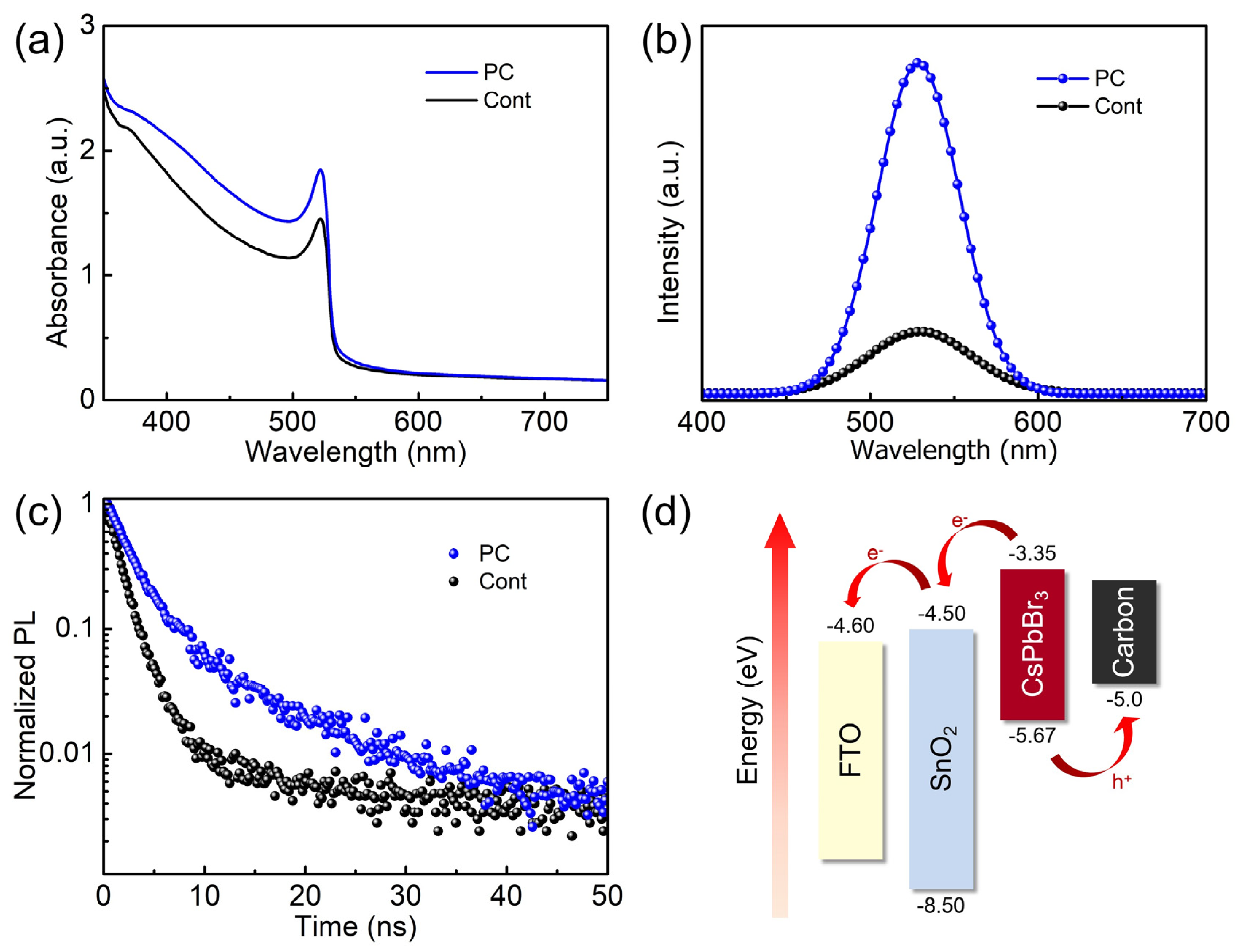
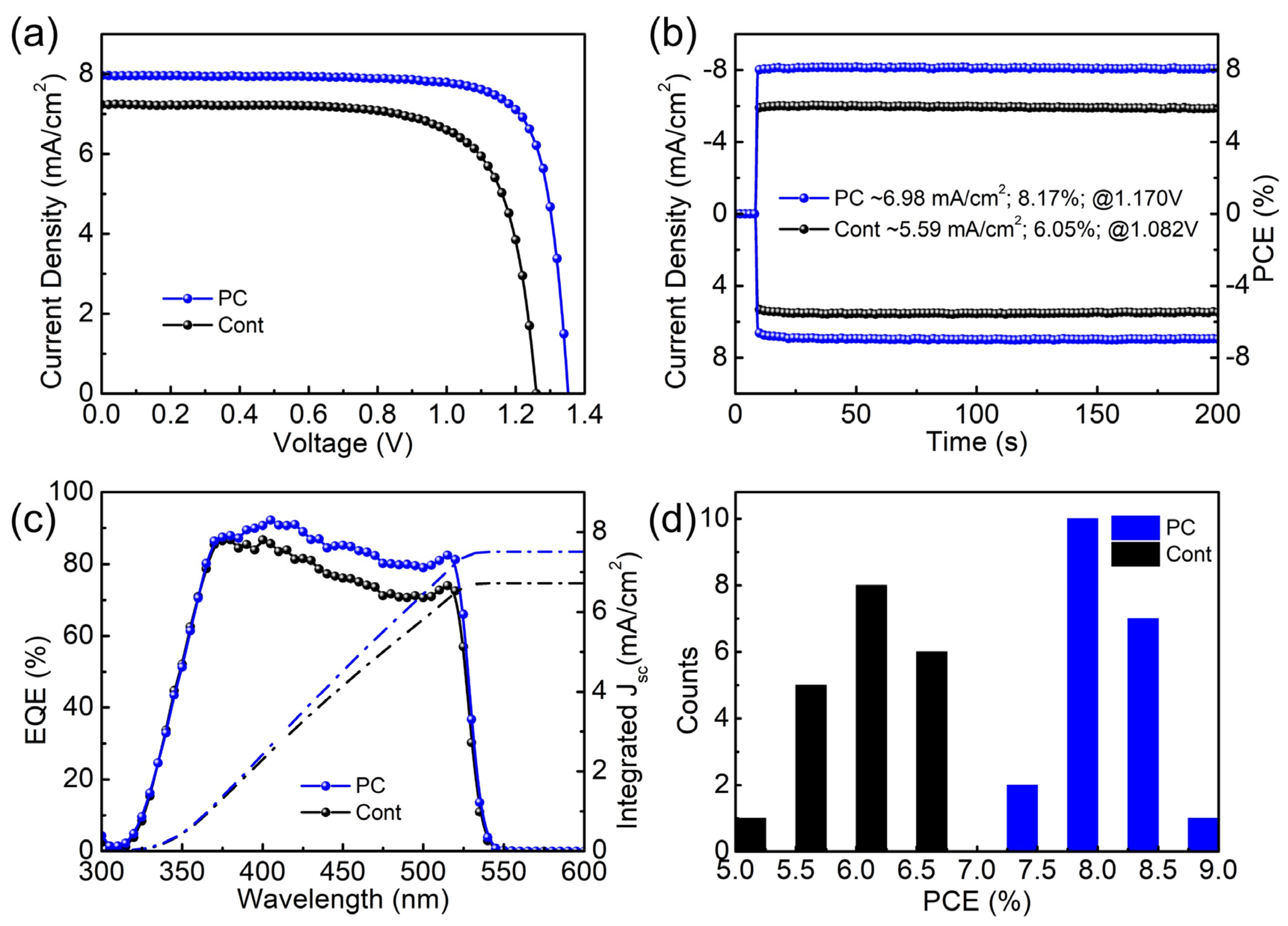
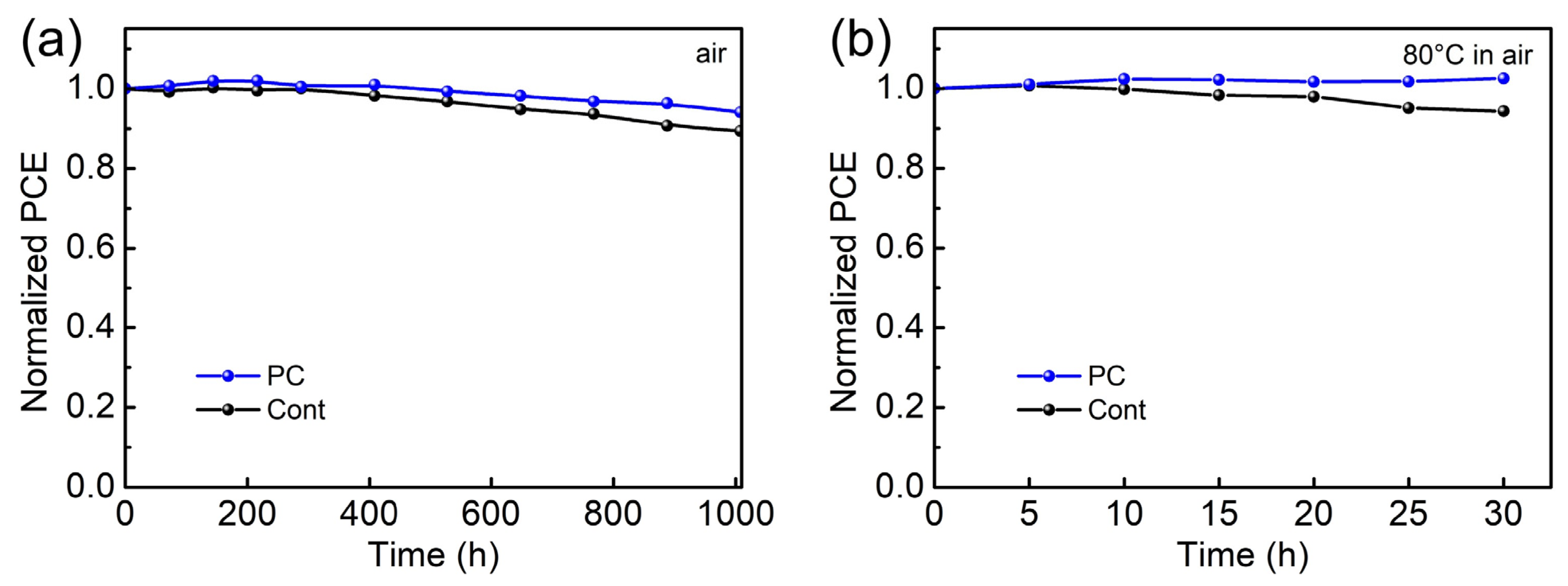
3. Results and Discussion

To investigate the influence of the pre-crystallization method on the morphology of PbBr2 precursor films and CsPbBr3 films, top-down angle scanning electron microscopy was employed for examination. Figure 1a presents the SEM images of untreated PbBr2 films as a control group, manifesting a relatively compact morphology along with a small number of pores. Figure 1b shows the SEM image of the PbBr2 film prepared by the pre-crystallization method. Upon comparison, it could be discerned that the PbBr2 film prepared using the pre-crystallization method displays more pores, featuring similar pore dimensions and uniform distribution. This porous configuration can leave diffusion channels for the second-step solution and enhance the contact area between the PbBr2 film and CsBr, thereby accelerating the reaction rate and increasing the crystal size of CsPbBr3 [26]. Figure 1c,d present the SEM images of untreated and pre-crystallized perovskite films. It can be observed that the pre-crystallization method renders the perovskite film more uniform, with a larger grain size and lower grain boundary density, with most crystal sizes exceeding 1 μm. Simultaneously, the pre-crystallization method enables CsPbBr3 to achieve a single-layer crystal structure in the longitudinal direction, as shown in Figure S1. These demonstrate that the pre-crystallization method can enhance the quality of perovskite films, thereby reducing non-radiative recombination phenomena and increasing the migration efficiency of charge carriers, ultimately effectively enhancing the photoelectric performance of PSCs [27].
Furthermore, the crystallization of PbBr2 and CsPbBr3 films was analyzed via X-ray diffraction spectroscopy testing. In Figure 2a, diffraction peaks situated at 18.7°, 21.7°, 30.3°, and 39.5° can be identified, which, respectively, correspond to the (020), (120), (130), and (140) crystal planes of PbBr2. Meanwhile, diffraction peaks at 11.7°, 23.3°, and 29.4° can also be noticed in the pre-crystallized PbBr2 film, corresponding to the (002), (210), and (213) crystal planes of CsPb2Br5, respectively. In the PbBr2 film prepared using the pre-crystallization method, a minor amount of CsPb2Br5 crystals was generated through the chemical reaction between PbBr2 and a small quantity of CsBr, as indicated in Equation (1). Additionally, in contrast to untreated perovskite films, the diffraction peak intensity of PbBr2 in the pre-crystallized samples was enhanced, particularly on the (020) and (120) crystal planes. The phase transition during the preparation of CsPbBr3 films using the multi-step spin-coating method can typically be depicted as the following chemical reactions [21]:
2PbBr2 + CsBr → CsPb2Br5 (with excess amount of PbBr2)
CsPb2Br5 + CsBr → 2CsPbBr3
CsPbBr3 + 3CsBr → Cs4PbBr6 (with excess amount of CsBr)
Figure 2b shows the X-ray diffraction spectra of perovskite films prepared using untreated and pre-crystallized methods. Diffraction peaks situated at 15.2°, 21.6°, 30.7°, 34.5°, 44.1°, and 49.6° can be conspicuously perceived in both untreated and pre-crystallized films, respectively corresponding to the (100), (110), (200), (210), (220), and (310) crystal planes of CsPbBr3. The CsPb2Br5 phase can still be detected in the untreated perovskite film, which represents a common phenomenon in the multi-step spin-coating method when PbBr2 is excessive [28]. After the employment of the pre-crystallization method, the CsPb2Br5 phase was mitigated, and diffraction peaks at 25.4°, 27.5°, and 28.6° were observed, respectively, corresponding to the (024), (131), and (214) crystal planes of CsPb4Br6. The phase of CsPb4Br6 is rather feeble, and the entire procedure is in accordance with Equations (1)–(3). Meanwhile, the pre-crystallization method also augmented the intensity of the CsPbBr3 diffraction peak. In the course of preparing the CsPbBr3 film using the pre-crystallization method, not only does the porous structure of the PbBr2 film accelerate the reaction rate with the CsBr solution, but also a small quantity of CsPb2Br5 crystals within the PbBr2 film function as nucleation sites to expedite the complete conversion of PbBr2 to CsPbBr3. Owing to the influence of the two factors, the pre-crystallized perovskite film exhibits better crystallinity and higher phase purity.
Figure 3a presents the UV-Vis absorption spectra of untreated and pre-crystallized CsPbBr3 films. The pre-crystallized perovskite film exhibits a significantly enhanced light-absorption capacity relative to the control group within the 350–535 nm range, and the absorption band edge corresponds to the 2.32 eV band gap of CsPbBr3, as shown in Figure S2. The enhancement of the light-absorption capability of the pre-crystallized sample mainly results from higher crystallinity, which is conducive to achieving a higher Jsc, in line with the measurement outcomes presented in Figure 2b.
Furthermore, the steady-state photoluminescence (PL) behavior of perovskite films was investigated. Figure 3b presents the steady-state PL spectrum of a perovskite film deposited directly onto an FTO substrate. Owing to the absence of ETL and HTL, excited state carriers cannot be promptly extracted, thereby leading to radiative recombination. Consequently, a higher fluorescence intensity suggests fewer traps or defects [29]. The pre-crystallized samples manifest a stronger PL emission peak intensity, indicating that the trap states in CsPbBr3 films are mitigated. The PL emission peaks of the control group and pre-crystallization were 531 nm and 529 nm, respectively. The minor blue shift of the emission peak can be accounted for by the passivation of near-band edge defects or sub-band gap defects [30], further substantiating that the pre-crystallization method can effectively minimize the defect states of CsPbBr3 films. Figure 3c shows the time-resolved PL (TRPL) spectrum of perovskite films, which can be appropriately fitted using a double exponential equation:
I(t) = A1 exp(−t/τ1) + A2 exp(−t/τ2)
Here, τ1 and τ2 denote the slow decay time constants and fast decay time constants, respectively. A1 and A2 stand for the relative amplitudes. Commonly, the slow decay component mirrors the trap-assisted radiation-recombination process within the perovskite crystal, whereas the fast decay component is associated with the quenching of charge carriers at the interface [31]. Table S1 recapitulates the TRPL parameters of two CsPbBr3 films. After the employment of the pre-crystallization method, the average carrier lifetime (τave) escalated from 3.57 ns to 7.32 ns, an increase of over 100%. The elongation of the carrier lifetime implies a reduction in defect density within perovskite films, attributable to higher crystallinity and a decrement in the grain boundary density engendered by larger grains [32]. This will enhance the efficiency of charge extraction and collection, facilitating the improvement in Jsc and Voc in the device.
A PSC with FTO/SnO2/CsPbBr3/carbon structure was fabricated by employing untreated and pre-crystallized CsPbBr3 films. The production process was conducted in an air environment, and the energy level diagram of the entire device is presented in Figure 3d. The cascaded conduction band arrangement between FTO, SnO2, and CsPbBr3 is beneficial for electron transfer and collection. Meanwhile, carbon has a higher valence band than CsPbBr3, which is conducive to electron blocking and hole extraction. The J-V characteristics of untreated and pre-crystallized devices under AM 1.5 G single solar irradiation (100 mW/cm2) are shown in Figure 4a. Table 1 summarizes the photovoltaic parameters of PSCs fabricated using untreated and pre-crystallized methods, including Jsc, Voc, FF, and PCE, with 20 devices fabricated for each type. The device based on untreated CsPbBr3 merely attained an average PCE of 5.97%, with the champion device achieving a 6.77% PCE, Jsc of 7.25 mA/cm2, Voc of 1.260 V, and FF of 0.741. After pre-crystallization treatment, all photovoltaic parameters were significantly enhanced, and the average PCE of the device was increased to 7.93%. The champion device presented a Jsc of 7.96 mA/cm2, Voc of 1.351 V, and FF of 0.802, attaining a high PCE of 8.62%. The improvement in device performance is mainly ascribed to the increased crystallinity, reduced defects, and extended carrier lifetime of CsPbBr3 films resulting from the pre-crystallization method. Additionally, due to the reduction in the grain boundary density, the pre-crystallization method can effectively mitigate hysteresis phenomena, as shown in Figure S3.
Figure 4b shows the steady-state output of the champion devices at their maximum power point. The photocurrent and PCE of both devices can rapidly attain their maximum values under illumination. The pre-crystallized device achieved a stable PCE of 8.17% at a bias voltage of 1.170 V, corresponding to a stable photocurrent density of 6.98 mA/cm2. This was significantly higher than the 6.05% PCE obtained by the control group device at a bias voltage of 1.082 V, corresponding to a photocurrent density of 5.59 mA/cm2. Additionally, after continuous illumination for 200 s, the PCE of the pre-crystallized device remained unchanged, demonstrating better stability. We also measured the incident photo-conversion efficiency (IPCE) spectrum of the champion device under short-circuit conditions, as presented in Figure 4c. Owing to the large bandgap of CsPbBr3, the devices predominantly respond to wavelengths within the range of 300–550 nm, showing a cutoff wavelength similar to Figure 3a at 535 nm. The pre-crystallized device exhibits higher quantum yields within the response range, resulting in a higher integrated current density than the untreated device. The current densities of the untreated and pre-crystallized devices were 6.72 mA/cm2 and 7.51 mA/cm2, respectively, slightly lower than the J-V results, attributed to the inherent properties of the perovskite film [33]. Furthermore, the PCEs of 20 devices fabricated by the untreated and pre-crystallization methods were statistically analyzed, as shown in Figure 4d. Compared with untreated devices, the pre-crystallization method can prepare more efficient photovoltaic devices more stably, and other photovoltaic parameters are also enhanced, as shown in Figure S4.
To explore the causes by which the pre-crystallization method enhances the performance of PSCs, the dark J-V characteristics were determined through the utilization of the structure of FTO/SnO2/CsPbBr3/PCBM/Carbon. The trap state density (ntrap) of CsPbBr3 films can be derived via the space charge limited current (SCLC) method, and the calculation equation is presented as follows [34]:
ntrap = 2εrε0VTFL/eL2
Here, εr is the relative dielectric constant of CsPbBr3 (εr = 16.64), where ε0 denotes the vacuum dielectric constant, VTFL refers to the limit voltage for trap filling, e symbolizes the fundamental charge of electrons, and L stands for the thickness of the perovskite film (L = 300 nm). As shown in Figure 5a, the VTFL of untreated and pre-crystallized devices are 1.16 V and 0.79 V, respectively. After calculation, following the utilization of the pre-crystallization method, the ntrap of the device has significantly decreased from 7.08 × 1015 cm−3 to 4.82 × 1015 cm−3. This implies that the pre-crystallization method is beneficial for reducing defects and traps in CsPbBr3 films.
Electrochemical impedance spectroscopy (EIS) measurements were also carried out to explore charge transfer and recombination in PSCs. Figure 5b presents the Nyquist plot of untreated and pre-crystallized devices under standard sunlight irradiation (100 mW/cm2) at a bias voltage of 0.8 V and within a frequency range from 1 MHz to 0.01 Hz. Two primary semicircles can be perceived in the figure. The small semicircle at high frequencies is connected to hole transport at the interface of perovskite/HTL or HTL/electrode, corresponding to charge transport resistance (Rct). The large semicircle at low frequencies is associated with the electron-recombination process at the SnO2/perovskite interface, corresponding to the charge in recombination resistance (Rrec) [35]. Compared to untreated devices, pre-crystallization decreases the Rct of the device from 214 Ω to 129 Ω, leading to more rapid charge extraction, as shown in Table S2. At the same time, the Rrec of the pre-crystallized device is 1887 Ω, higher than that of the untreated device at 1171 Ω, indicating a lower recombination rate. Faster charge extraction and lower carrier recombination lead to higher Jsc and Voc for pre-crystallized devices. In addition, it can be deduced from the starting point in the real part of the Nyquist plot that the series resistance (Rs) of the pre-crystallized device is 37.2 Ω, which is lower than the 42.1 Ω of the untreated device, which means that the conductivity of the pre-crystallized perovskite film is higher and the charge-transport capacity is stronger, facilitating the attainment of higher FF [36].
Finally, the stability of the device was examined. In an environment with a temperature of 20 °C and a relative humidity (RH) of 20%, untreated and pre-crystallized devices demonstrate excellent stability, as presented in Figure 6a. This is ascribed to the outstanding environmental stability of CsPbBr3, and the carbon electrode also contributes to enhancing the long-term stability of the device [37,38]. The pre-crystallized device can still retain an initial value of over 94% after 1000 h, pointing out that the pre-crystallization method can effectively enhance the stability of the CsPbBr3 device. In a high-temperature environment (80 °C, 20% RH), the pre-crystallized device also manifested superior thermal stability without significant degradation, as shown in Figure 6b.

4. Conclusions

In summary, during the multi-step fabrication process of CsPbBr3 perovskite solar cells, we employed a pre-crystallization method. By introducing a minor quantity of CsBr into the precursor solution of PbBr2, mesoporous PbBr2 films containing a small amount of CsPb2Br5 crystals were produced. A series of test results indicated that the CsPbBr3 films prepared using the pre-crystallization method possess larger crystal sizes, lower grain boundary density, enhanced crystallinity, and higher phase purity. This reduces the trap state density of perovskite films, effectively facilitating charge transfer and suppressing carrier recombination. The device fabricated using the pre-crystallization method achieved a champion PCE of 8.62%, which is 27% higher than that of the untreated device. Additionally, the pre-crystallized devices demonstrate superior stability and thermal stability.

Supplementary Materials

The following supporting information can be downloaded at: https://www.mdpi.com/article/10.3390/coatings14070918/s1, Table S1: Parameters of the TR-PL spectroscopy for the CsPbBr3 samples with varied CsBr spin-coating cycles. Table S2: EIS parameters of various CsPbBr3 PSCs in the dark condition. Figure S1: Cross-sectional SEM image of the pre-crystallized CsPbBr3 film. Figure S2: Tauc diagram of CsPbBr3 films. Figure S3: Forward and reverse scanning J-V curves of (a) untreated and (b) pre-crystallized devices. Figure S4: Box plots of (a) Jsc, (b) Voc, (c) FF, and (d) PCE of untreated and pre-crystallized PSCs, respectively. Each group is fabricated with 20 devices.

Author Contributions

Conceptualization, Y.Z., Z.J. and W.Z.; methodology, Y.Z.; software, J.L.; validation, J.L.; formal analysis, Y.Z.; investigation, Y.Z.; resources, G.M. and J.G.; data curation, Y.Z.; writing—original draft preparation, Y.Z.; writing—review and editing, Y.Z.; visualization, supervision, Z.J.; project administration, Z.J.; funding acquisition, Z.J. and W.Z. All authors have read and agreed to the published version of the manuscript.

Funding

This research was funded by TAIYUAN UNIVERSITY OF SCIENCE AND TECHNOLOGY SCIENTIFIC RESEARCH INITIAL FUNDING, grant number 20232091.

Institutional Review Board Statement

Not applicable.

Informed Consent Statement

Not applicable.

Data Availability Statement

Data are contained within the article/Supplementary Material; further inquiries can be directed to the corresponding author.

Acknowledgments

We gratefully acknowledge Beihang University and Hangzhou Acme Optoelectronics Technology Co., Ltd. for providing access to their experimental equipment to fabricate samples and their measurements.

Conflicts of Interest

Author Guanxiong Meng, Jiajun Guo were employed by Hangzhou Acme Optoelectronics Technology Co., Ltd. The remaining authors declare that the research was conducted in the absence of any commercial or financial relationships that could be construed as a potential conflict of interest.

References

  1. Kojima, A.; Teshima, K.; Shirai, Y.; Miyasaka, T. Organometal halide perovskites as visible-light sensitizers for photovoltaic cells. J. Am. Chem. Soc. 2009, 131, 6050–6051. [Google Scholar] [CrossRef] [PubMed]
  2. Zhou, J.; Tan, L.; Liu, Y.; Li, H.; Liu, X.; Li, M.; Wang, S.; Zhang, Y.; Jiang, C.; Hua, R.; et al. Highly efficient and stable perovskite solar cells via a multifunctional hole transporting material. Joule 2014, 8, 1691–1706. [Google Scholar] [CrossRef]
  3. Heo, D.Y.; Lee, T.H.; Iwan, A.; Kavan, L.; Omatova, M.; Majkova, E.; Kamarás, K.; Jang, H.W.; Kim, S.Y. Effect of lead thiocyanate ions on performance of tin-based perovskite solar cells. J. Power Sources 2022, 458, 228067. [Google Scholar] [CrossRef]
  4. Tian, X.; Stranks, S.D.; You, F. Life cycle assessment of recycling strategies for perovskite photovoltaic modules. Nat. Sustain. 2021, 4, 821–829. [Google Scholar] [CrossRef]
  5. Yang, Y.; You, J. Make perovskite solar cells stable. Nature 2017, 544, 155–156. [Google Scholar] [CrossRef] [PubMed]
  6. Wang, L.; Shahiduzzaman, M.; Muslih, E.Y.; Nakano, M.; Karakawa, M.; Takahashi, K.; Tomita, K.; Nunzi, J.M.; Taima, T. Double-layer CsI intercalation into an MAPbI3 framework for efficient and stable perovskite solar cells. Nano Energy 2021, 86, 106135. [Google Scholar] [CrossRef]
  7. Liu, Q.; Qiu, J.; Yan, X.; Fei, Y.; Qiang, Y.; Chang, Q.; Wei, Y.; Zhang, X.; Tian, W.; Jin, S.; et al. Surface passivation and hole extraction: Bifunctional interfacial engineering toward high-performance all-inorganic CsPbIBr2 perovskite solar cells with efficiency exceeding 12%. J. Energy Chem. 2022, 74, 387–393. [Google Scholar] [CrossRef]
  8. Qiu, J.; Mei, X.; Zhang, M.; Wang, G.; Zou, S.; Wen, L.; Huang, L.; Hua, Y.; Zhang, X. Dipolar Chemical Bridge Induced CsPbI3 Perovskite Solar Cells with 21.86 % Efficiency. Angew. Chem. Int. Ed. 2024, 63, e202401751. [Google Scholar] [CrossRef]
  9. Wang, Z.; Tian, Q.; Zhang, H.; Xie, H.; Du, Y.; Liu, L.; Feng, X.; Najar, A.; Ren, X.; Liu, S. Managing Multiple Halide-Related Defects for Efficient and Stable Inorganic Perovskite Solar Cells. Angew. Chem. Int. Ed. 2023, 62, e202305815. [Google Scholar] [CrossRef]
  10. Cheng, J.; Fan, Z.; Dong, J. Research Progress of Green Solvent in CsPbBr3 Perovskite Solar Cells. Nanomaterials 2023, 13, 991. [Google Scholar] [CrossRef]
  11. Sutton, R.J.; Eperon, G.E.; Miranda, L.; Parrott, E.S.; Kamino, B.A.; Patel, J.B.; Hörantner, M.T.; Johnston, M.B.; Haghighirad, A.A.; Moore, D.T.; et al. Bandgap-tunable cesium lead halide perovskites with high thermal stability for efficient solar cells. Adv. Energy Mater. 2016, 6, 1502458. [Google Scholar] [CrossRef]
  12. Wei, L.; Rothmann, M.U.; Liu, A.; Wang, Z.; Zhang, Y.; Pascoe, A.R.; Lu, J.; Jiang, L.; Chen, Y.; Huang, F.; et al. Phase segregation enhanced ion movement in efficient inorganic CsPbIBr2 solar cells. Adv. Energy Mater. 2017, 7, 1700946. [Google Scholar] [CrossRef]
  13. Duan, J.; Zhao, Y.; He, B.; Tang, Q. High-purity inorganic perovskite films for solar cells with 9.72% efficiency. Angew. Chem. Int. Ed. 2018, 57, 3787–3791. [Google Scholar] [CrossRef] [PubMed]
  14. Liang, J.; Wang, C.; Wang, Y.; Xu, Z.; Lu, Z.; Ma, Y.; Zhu, H.; Hu, Y.; Xiao, C.; Yi, X.; et al. All-inorganic perovskite solar cells. J. Am. Chem. Soc. 2016, 138, 15829–15832. [Google Scholar] [CrossRef]
  15. Zhu, J.; Tang, M.; He, B.; Shen, K.; Zhang, W.; Sun, X.; Sun, M.; Chen, H.; Duan, Y.; Tang, Q. Ultraviolet filtration and defect passivation for efficient and photostable CsPbBr3 perovskite solar cells by interface engineering with ultraviolet absorber. Chem. Eng. J. 2021, 404, 126548. [Google Scholar] [CrossRef]
  16. Liang, K.; Wu, Y.; Zhen, Q.; Zou, Y.; Zhang, X.; Wang, C.; Shi, P.; Zhang, Y.; Sun, W.; Li, Y.; et al. Solvent vapor annealing-assisted mesoporous PbBr2 frameworks for high-performance inorganic CsPbBr3 perovskite solar cells. Surf. Interfaces 2023, 37, 102707. [Google Scholar] [CrossRef]
  17. Cao, X.; Zhang, G.; Su, G.; Zhang, H.; Song, W.; Xie, X.; Wang, Y.; Zeng, Q.; He, X.; Wei, J. Fabrication of large columnar grains composed CsPbBr3 films for efficient solar cells through ligand engineering. Colloids Surf. A Physicochem. Eng. Asp. 2023, 674, 131817. [Google Scholar] [CrossRef]
  18. Zhao, Y.; Wang, S.; Ran, H.; Zhang, Y.; Tang, Y. Two-in-one additive engineering strategy induced high-quality CsPbBr3 film in printable mesoscopic perovskite solar cells. J. Alloys Compd. 2023, 965, 171317. [Google Scholar] [CrossRef]
  19. Che, G.; Wang, X.; Cui, C.; Pang, B.; Wang, X.; Dong, H.; Feng, J.; Yu, L.; Dong, L. Boosting the efficiency and stability of CsPbBr3 perovskite solar cells through modified multi-step spin-coating method. J. Alloys Compd. 2023, 969, 172423. [Google Scholar] [CrossRef]
  20. Chi, K.; Zhai, Y.; Wang, Y.; Zhang, X.; Liang, F.; Wang, S. Porous PbBr2 films modulation by indium tribromide additive for the fabrication of SnO2-based CsPbBr3 perovskite solar cells. Ceram. Int. 2024, 50, 28386–28393. [Google Scholar] [CrossRef]
  21. Liu, X.; Tan, X.; Liu, Z.; Ye, H.; Sun, B.; Shi, T.; Tang, Z.; Liao, G. Boosting the efficiency of carbon-based planar CsPbBr3 perovskite solar cells by a modified multistep spin-coating technique and interface engineering. Nano Energy 2019, 56, 184–195. [Google Scholar] [CrossRef]
  22. Liu, X.; Liu, Z.; Tan, X.; Ye, H.; Sun, B.; Xi, S.; Shi, T.; Tang, Z.; Liao, G. Novel antisolvent-washing strategy for highly efficient carbon-based planar CsPbBr3 perovskite solar cells. J. Power Sources 2019, 439, 227092. [Google Scholar] [CrossRef]
  23. Yan, J.; Hou, S.; Li, X.; Dong, J.; Zou, L.; Yang, M.; Xing, J.; Liu, H.; Hao, H. Preparation of highly efficient and stable CsPbBr3 perovskite solar cells based on an anti-solvent rinsing strategy. Sol. Energy Mater. Sol. Cells 2022, 234, 111420. [Google Scholar] [CrossRef]
  24. Chen, D.; He, Y.; Fan, G.; Zhang, Z.; Zhu, W.; Xi, H.; Zhou, L.; Zhang, C.; Zhang, J.; Hao, Y. Ultrahigh fill-factor all-inorganic CsPbBr3 perovskite solar cells processed from two-step solution method and solvent additive strategy. J. Mater. 2023, 9, 717–724. [Google Scholar] [CrossRef]
  25. Zhang, Y.; Jiang, Z.; Zhang, W.; Yan, L.; Lu, C.; Ni, C. Pre-crystallization applied in two-step spin-coating method for high-quality perovskite films in photovoltaic devices. J. Alloys Compd. 2020, 832, 153616. [Google Scholar] [CrossRef]
  26. Zhao, Y.; Duan, J.; Wang, Y.; Yang, X.; Tang, Q. Precise stress control of inorganic perovskite films for carbon-based solar cells with an ultrahigh voltage of 1.622 V. Nano Energy 2020, 67, 104286. [Google Scholar] [CrossRef]
  27. Liu, J.; Zhu, L.; Xiang, S.; Wei, Y.; Xie, M.; Liu, H.; Li, W.; Chen, H. Growing high-quality CsPbBr3 by using porous CsPb2Br5 as an intermediate: A promising light absorber in carbon-based perovskite solar cells. Sustain. Energy Fuels 2019, 3, 184–194. [Google Scholar] [CrossRef]
  28. Teng, P.; Han, X.; Li, J.; Xu, Y.; Kang, L.; Wang, Y.; Yang, Y.; Yu, T. Elegant Face-Down Liquid-Space-Restricted Deposition of CsPbBr3 Films for Efficient Carbon-Based All-Inorganic Planar Perovskite Solar Cells. ACS Appl. Mater. Interfaces 2018, 10, 9541. [Google Scholar] [CrossRef] [PubMed]
  29. Luo, J.; Jia, C.; Wan, Z.; Han, F.; Zhao, B.; Wang, R. The novel dopant for hole-transporting material opens a new processing route to efficiently reduce hysteresis and improve stability of planar perovskite solar cells. J. Power Sources 2017, 342, 886–895. [Google Scholar] [CrossRef]
  30. Cao, X.; Zhang, G.; Cai, Y.; Jiang, L.; Chen, Y.; He, X.; Zeng, Q.; Jia, Y.; Xing, G.; Wei, J. Enhanced performance of CsPbBr3 perovskite solar cells by reducing the conduction band offsets via a Sr-modified TiO2 layer. Appl. Surf. Sci. 2020, 529, 147119. [Google Scholar] [CrossRef]
  31. Liu, X.; Liu, Z.; Ye, H.; Tu, Y.; Sun, B.; Tan, X.; Shi, T.; Tang, Z.; Liao, G. Novel efficient C60-based inverted perovskite solar cells with negligible hysteresis. Electrochim. Acta 2018, 288, 115–125. [Google Scholar] [CrossRef]
  32. Duan, J.; Zhao, Y.; Yang, X.; Wang, Y.; He, B.; Tang, Q. Lanthanide ions doped CsPbBr3 halides for HTM-free 10.14%-efficiency inorganic perovskite solar cell with an ultrahigh open-circuit voltage of 1.594 V. Adv. Energy Mater. 2018, 8, 1802346. [Google Scholar] [CrossRef]
  33. Saliba, M.; Etgar, L. Current density mismatch in perovskite solar cells. ACS Energy Lett. 2020, 5, 2886–2888. [Google Scholar] [CrossRef]
  34. Wang, S.; Wang, P.; Chen, B.; Li, R.; Ren, N.; Li, Y.; Shi, B.; Huang, Q.; Zhao, Y.; Grätzel, M.; et al. Suppressed recombination for monolithic inorganic perovskite/silicon tandem solar cells with an approximate efficiency of 23%. eScience 2022, 2, 339–346. [Google Scholar] [CrossRef]
  35. Wang, D.; Li, W.; Du, Z.; Li, G.; Sun, W.; Wu, J.; Lan, Z. Highly efficient CsPbBr3 planar perovskite solar cells via additive engineering with NH4SCN. ACS Appl. Mater. Interfaces 2020, 12, 10579–10587. [Google Scholar] [CrossRef] [PubMed]
  36. Hauff, E.; Klotz, D. Impedance spectroscopy for perovskite solar cells: Characterisation, analysis, and diagnosis. J. Mater. Chem. C 2022, 10, 742–761. [Google Scholar] [CrossRef]
  37. Cao, X.; Zhang, G.; Jiang, L.; Cai, Y.; Wang, Y.; He, X.; Zeng, Q.; Chen, J.; Jia, L.; Wei, J. Achieving environment-friendly production of CsPbBr3 films for efficient solar cellsviaprecursor engineering. Green Chem. 2021, 23, 2104–2112. [Google Scholar] [CrossRef]
  38. Fu, Z.; Xu, M.; Sheng, Y.; Yan, Z.; Meng, J.; Tong, C.; Li, D.; Wan, Z.; Ming, Y.; Mei, A.; et al. Encapsulation of Printable Mesoscopic Perovskite Solar Cells Enables High Temperature and Long-Term Outdoor Stability. Adv. Funct. Mater. 2019, 29, 1809129. [Google Scholar] [CrossRef]
Figure 1. Top-view SEM images of (a) untreated and (b) pre-crystallized PbBr2 films and (c) untreated and (d) pre-crystallized perovskite films.
Coatings 14 00918 g001
Figure 2. X-ray diffraction spectroscopy patterns of (a) PbBr2 films and (b) CsPbBr3 films.
Coatings 14 00918 g002
Figure 3. (a) Absorption spectrum, (b) steady-state PL spectrum, (c) TRPL spectrum, and (d) energy level diagram of photovoltaic devices for control and pre-crystallized perovskite films.
Coatings 14 00918 g003
Figure 4. (a) J-V curves of CsPbBr3 solar cells, (b) steady-state photocurrent and PCE at maximum output point voltage, (c) IPCE spectra and corresponding integrated Jsc, and (d) PCE distribution of 20 devices fabricated by control group and pre-crystallization method, respectively.
Coatings 14 00918 g004
Figure 5. (a) SCLC plots and (b) Nyquist plot of untreated and pre-crystallized PSCs in dark environment.
Coatings 14 00918 g005
Figure 6. Long-term stability of the untreated and pre-crystallized devices in (a) 20 °C air (relative humidity of 20%) and (b) thermal stability in 80 °C air.
Coatings 14 00918 g006
Table 1. Photovoltaic parameters of the untreated and pre-crystallized PSCs, with 20 prepared for each device.
Device Jsc (mA/cm2)Voc (V)FFPCE (%)
NoneAverage7.01 ± 0.721.210 ± 0.0730.723 ± 0.0415.97 ± 0.80
Champion7.251.2600.7416.77
PCAverage7.66 ± 0.521.292 ± 0.0630.787 ± 0.0297.93 ± 0.69
Champion7.961.3510.8028.62
Disclaimer/Publisher’s Note: The statements, opinions and data contained in all publications are solely those of the individual author(s) and contributor(s) and not of MDPI and/or the editor(s). MDPI and/or the editor(s) disclaim responsibility for any injury to people or property resulting from any ideas, methods, instructions or products referred to in the content.

