Article

Influence of Oxygen Flow Rate on the Phase Structures and Properties for Copper Oxide Thin Films Deposited by RF Magnetron Sputtering

1
School of Materials Science and Engineering, Pusan National University, Busan 46241, Republic of Korea
2
Department of Materials Science and Engineering, Silla University, Busan 46958, Republic of Korea
*
Author to whom correspondence should be addressed.
Coatings 2024, 14(8), 930; https://doi.org/10.3390/coatings14080930
Submission received: 17 June 2024 / Revised: 17 July 2024 / Accepted: 21 July 2024 / Published: 25 July 2024
(This article belongs to the Special Issue Magnetron Sputtering Coatings: From Materials to Applications)

Abstract

:
This study examines the impact of varying oxygen flow rates on the properties of Cu2O thin films deposited via radio frequency (RF) magnetron sputtering. X-ray diffraction (XRD) analysis showed a phase transition from cubic Cu2O to a mixed Cu2O and CuO phase, eventually forming a Cu4O3 tetragonal structure as oxygen content increased. The surface morphology and cross-sectional structure of Cu2O thin films observed through field emission scanning electron microscopy (FE-SEM) were found to vary significantly depending on the oxygen flow rate. X-ray photoelectron spectroscopy (XPS) indicated notable variations in the chemical states of copper and oxygen. The Cu 2p spectra revealed peaks around 933 eV and 953 eV for all samples, with the S01 sample (deposited with only argon gas) exhibiting the lowest intensity. The S02 sample showed the highest peak intensity, which then gradually decreased from S03 to S06. The O 1s spectra followed a trend with peak intensity being highest in S02 and decreasing with further oxygen flow rates, indicating the formation of complex oxides such as Cu4O3. UV-Vis-NIR spectroscopy results demonstrated a decrease in transmittance and optical band gap energy with increasing oxygen content, suggesting a decline in crystallinity and an increase in defects and impurities. These findings underscore the critical role of precise oxygen flow rate control in tailoring the structural, morphological, compositional, and optical properties of Cu2O thin films for specific electronic and optical applications.

1. Introduction

Copper(I) oxide (Cu2O) emerges as a highly promising semiconductor material for optoelectronic and photovoltaic applications owing to its chemical safety, non-toxicity, and direct band gap properties ranging from 2.1 to 2.6 eV [1,2,3,4,5]. With abundant reserves and cost-effectiveness, Cu2O stands as a competitive material [6]. Moreover, as a non-stoichiometric p-type material, its electrical characteristics are influenced by copper vacancies and oxygen interstitial atoms. Its high absorption coefficient renders it suitable for a diverse array of optoelectronic devices, such as solar cells and water-splitting photoanodes [7,8]. Among various deposition techniques, RF magnetron sputtering offers advantages in controlling the crystallinity, morphology, and thickness of Cu2O thin films alongside a straightforward process and large-area deposition capability [2,9,10].
While CuO exhibits higher absorbance across a broader wavelength range than Cu2O, both oxides hold potential for solar cell applications. However, Cu2O presents a transparency advantage within the visible spectrum, making it appealing for transparent electronics [11]. Despite these merits, Cu2O-based solar cells and sensors have not achieved anticipated efficiencies in the visible light spectrum due to their wide band gap [12]. Cu4O3, an intermediate phase between CuO and Cu2O, contains equivalent quantities of Cu(II) and Cu(I) ions, possessing distinct properties [12,13]. Arising from copper ore oxidation, Cu4O3 boasts excellent electrical and thermal conductivity, finding utility in electrical and electronic devices, catalysts, and antioxidants [14]. Despite various production methods, including laser ablation, solvothermal synthesis, and reactive sputtering, the production of Cu4O3 remains challenging [7,15].
In this study, crystalline Cu4O3 thin films were successfully deposited via magnetron sputtering by precisely controlling the oxygen flow rate [16] utilizing a Cu2O target. The primary objective of this research is to systematically explore the optimal conditions for RF magnetron sputtering to produce high-quality Cu2O thin films. By systematically varying the oxygen–argon gas ratio during deposition, we investigate its impact on the crystallographic structure, surface morphology, and compositional and optical properties of the films. Through this approach, we aim to identify the ideal parameters that maximize the efficiency of Cu2O-based devices in optoelectronic applications. Furthermore, the significance of this research extends beyond the immediate optimization of deposition parameters. Understanding the relationship between deposition conditions and film properties will contribute to the broader field of semiconductor research, offering insights into the development of other oxide-based materials. Additionally, the findings from this study could lead to advancements in the production of environmentally friendly and cost-effective optoelectronic devices, aligning with global sustainability goals.

2. Materials and Methods

2.1. Preparation of Cu2O Thin Films

Cu2O thin films were deposited on soda–lime glass, measuring 20 mm × 20 mm, utilizing a 99.99% pure Cu2O target through RF magnetron sputtering. The target-to-substrate distance was maintained at 130 mm. Prior to deposition, the glass substrates were meticulously cleaned to remove contaminants. The meticulous cleaning process was essential to ensure the removal of organic and inorganic contaminants, which could otherwise affect the adhesion and quality of the deposited Cu2O thin films. The cleaning process involved blowing off dust with nitrogen (N2), soaking in distilled water, and ultrasonic washing for 5 min. The substrates were then soaked in acetone and subjected to another 5 min ultrasonic wash, followed by rinsing with distilled water. This was repeated with ethanol and isopropyl alcohol, each followed by a 5 min ultrasonic wash and a final rinse with distilled water. The cleaned glass substrates were dried using an N2 gun. To remove residual organic contaminants from the surface of the glass substrates prepared in this way and to improve thin film adhesion, UV-ozone cleaning was finally performed for 20 min.
For the deposition process, the cleaned glass substrates were placed in a load lock chamber, evacuated to 8 × 10⁻² Torr (10.7 Pa), and then transferred to the main chamber. In the main chamber, the pressure was reduced to 8 × 10⁻³ Torr (1.1 Pa) under low vacuum and further to 3 × 10⁻⁶ Torr (4 × 10⁻⁴ Pa) under high vacuum. The deposition temperature was maintained at 350 °C using a mixed gas of high-purity argon (Ar) and 5% oxygen (O2) [Ar + O2 (5%)]. Maintaining the deposition temperature at 350°C was critical for ensuring good crystallinity and phase purity of the Cu2O thin films. The gas flow was regulated through a mass flow controller (MFC), and 20 sccm of Ar gas was used to create the initial sputtering atmosphere. Oxygen gas was then introduced to achieve a combined gas flow of 20 sccm, with the following gas flow ratios for the samples: S01 (Ar 20 sccm), S02 (Ar 18 sccm + O2 2 sccm), S03 (Ar 16 sccm + O2 4 sccm), S04 (Ar 14 sccm + O2 6 sccm), S05 (Ar 12 sccm + O2 8 sccm), and S06 (Ar 10 sccm + O2 10 sccm). Plasma was generated by increasing the RF power while maintaining the pressure in the chamber at 4 × 10⁻² Torr (5.3 Pa). The RF power was gradually increased to 55 W, followed by adjusting the working pressure to 5 × 10⁻³ Torr (6.7 × 10⁻¹ Pa) and pre-sputtering for 30 min. The gradual increase in RF power and the pre-sputtering step were implemented to stabilize the plasma and clean the target surface, respectively. Subsequently, the shutter was opened, and a Cu2O thin film was deposited on the substrate for 90 min. The 90 min deposition time was chosen based on preliminary experiments that indicated this duration was sufficient to achieve the desired film thickness while maintaining uniformity and structural integrity.

2.2. Characterization Techniques

To evaluate the properties of the fabricated thin films, comprehensive analyses were conducted using X-ray diffraction (XRD, SmartLab, RIGAKU, KOREA I.T.S, Seoul, Republic of Korea), Raman spectroscopy (RAMANtouch, Nanophoton, Tokyo, Japan), field emission scanning electron microscopy (FE-SEM, SU8200, Hitachi, Tokyo, Japan), X-ray photoelectron spectroscopy (XPS, K-Alpha, Thermo Fisher Scientific Korea, Seoul, Republic of Korea), and ultraviolet–visible–near-infrared spectrophotometry (UV–Vis–NIR, V-570, JASCO, Easton, MD, USA). XRD analyses were performed to determine the crystalline structure and phase composition of the thin films. XRD patterns were obtained with Cu Kα radiation (λ = 1.5406 Å), scanned over a 2θ range from 20° to 80° at a scan rate of 2° per minute. FE-SEM was utilized to examine the surface morphology and microstructural features of the films. FE-SEM images were acquired at an accelerating voltage of 10 kV. XPS was employed to analyze the chemical composition and oxidation states of the elements within the thin films, and the spectra were obtained with a monochromatic Al Kα X-ray source (1486.6 eV). The binding energies were calibrated using the C 1s peak at 284.8 eV as a reference. The UV–Vis–NIR equipment was used to measure the optical properties of the films, including transmittance and absorbance. The measurements were taken over a wavelength range of 400 to 2000 nm.

3. Results and Discussion

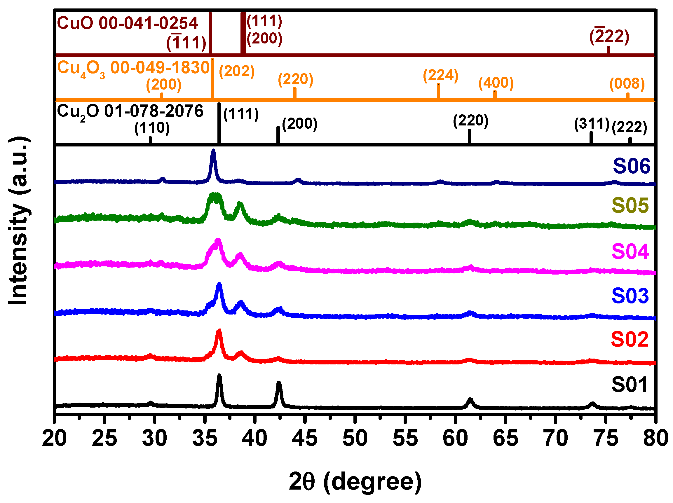
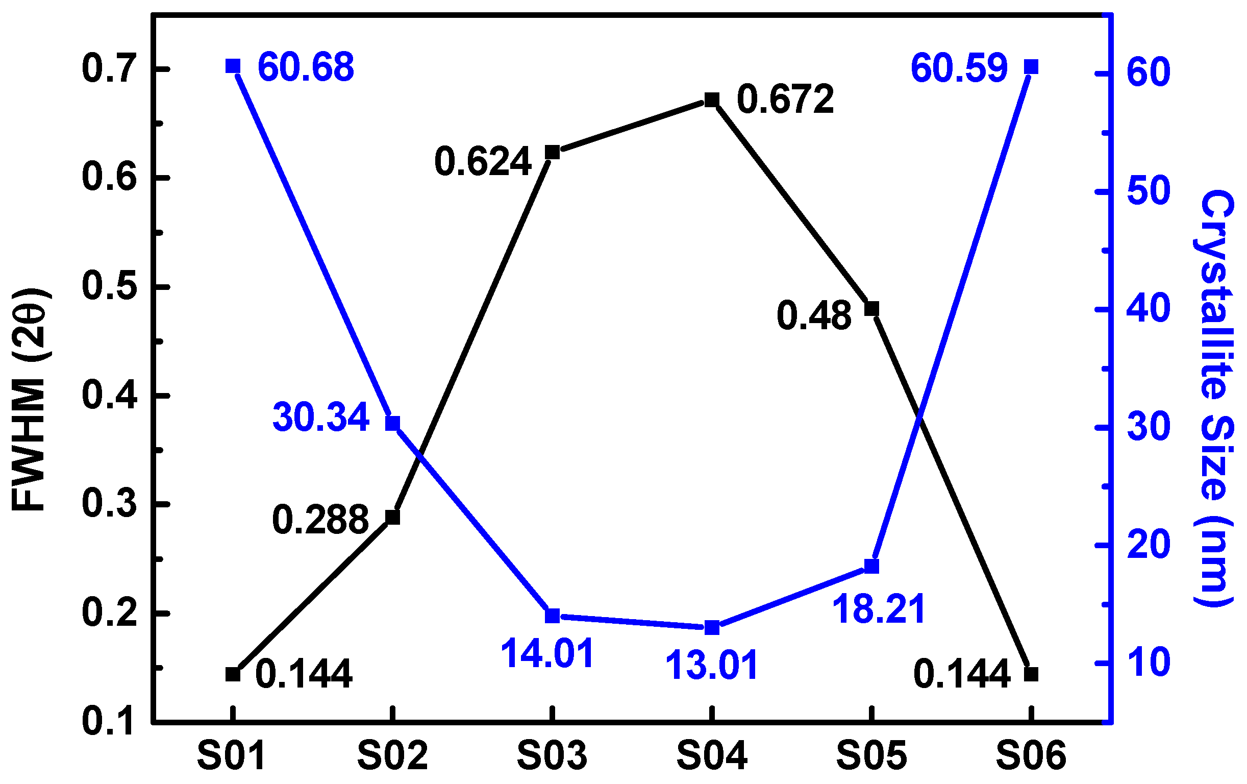
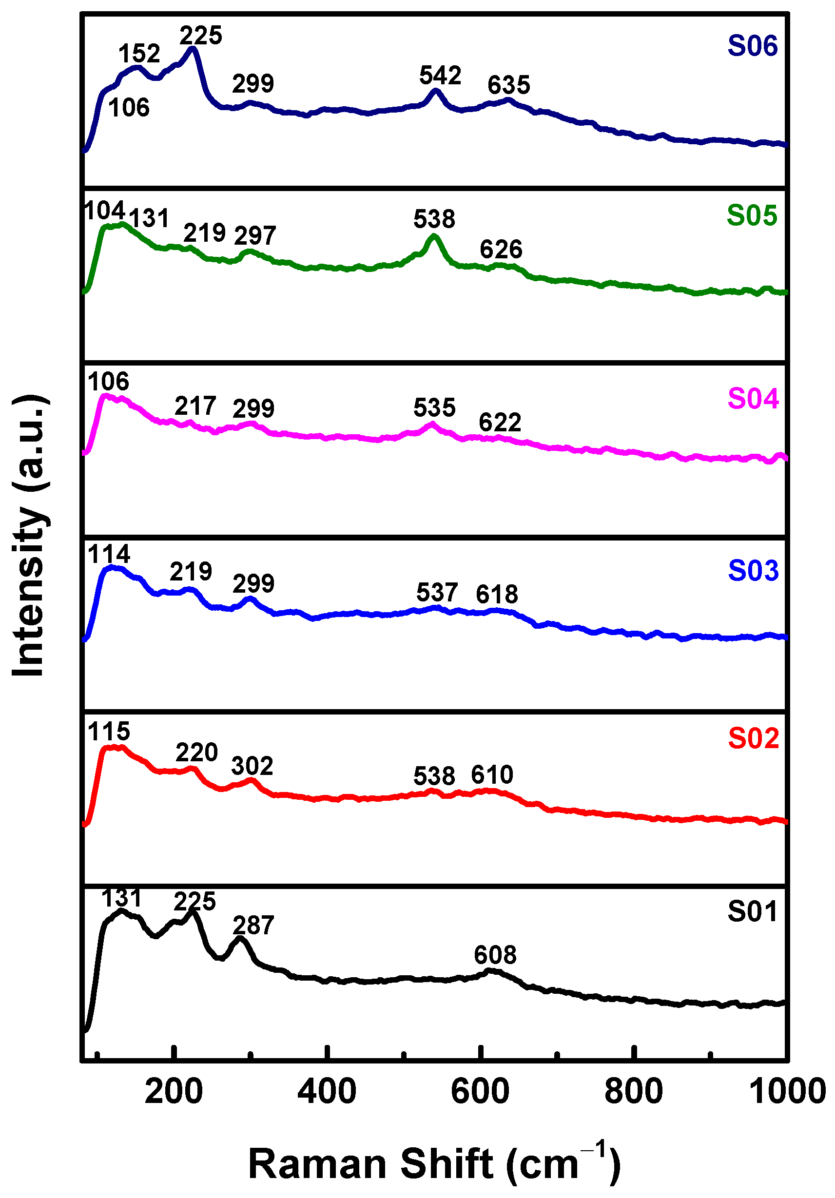
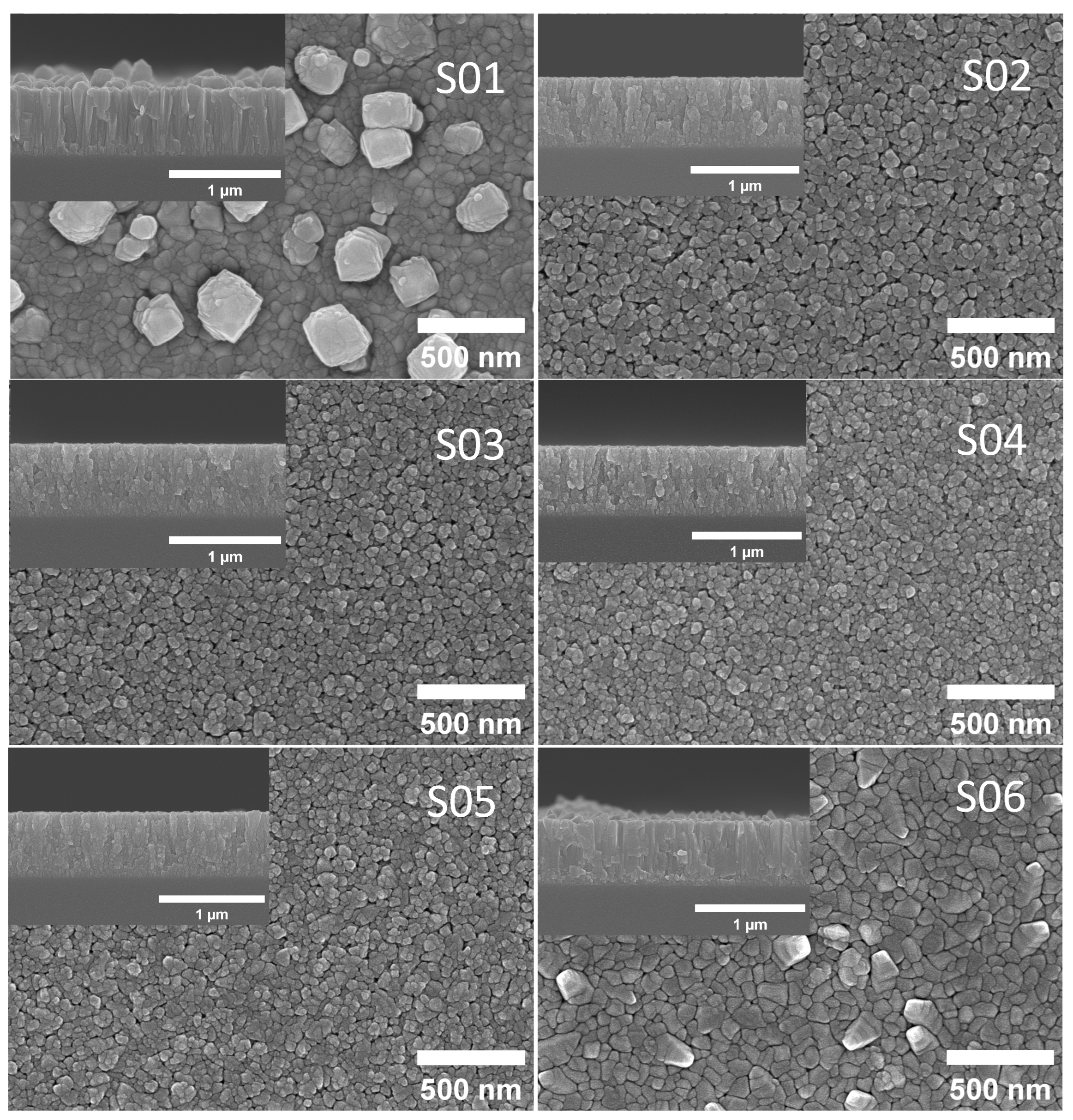
3.1. Structural Properties of Cu2O Thin Films

The crystal structure of the Cu2O thin films was confirmed through X-ray diffraction (XRD) analysis, and the corresponding results are presented in Figure 1. In Figure 1, the diffraction pattern of the Cu2O film grown by injecting only 20 sccm of Ar gas was indicated as S01. The preferential growth orientation of the S01 sample was the (111) plane, corresponding to a 2θ diffraction angle of 36.4°. The diffraction peak with the second strongest intensity was observed at 42.3°, and relatively weaker peaks were revealed at 29.6°, 61.4°, and 73.6°. The observed peaks correspond to the (110), (200), (220), and (311) planes, indicating that the Cu2O thin film was grown in a cubic crystal structure (ICDD No. 01-078-2076) [15].
The XRD patterns of Cu2O thin films sputtered at various mixed gas flow ratios (O2/Ar + O2) are presented from S02 to S06 samples. Compared to the S01 sample with an oxygen gas flow ratio of 0%, the intensity of all peaks representing the Cu2O crystalline structure in the S02 to S05 samples decreased as the flow ratio increased from 10% to 40%. In the XRD pattern of the S06 sample with an oxygen gas flow ratio of 50%, diffraction peaks corresponding to the (200), (202), (220), (224), (400), and (008) planes emerged, which had not been observed previously. These peaks precisely aligned with diffraction angles of 30.7°, 35.8°, 43.9°, 58.3°, 63.9°, and 77.2°, signifying the transformation of Cu2O to a Cu4O3 tetragonal structure (ICDD No. 00-049-1830) [17]. Additionally, we observed the coexistence of Cu2O and CuO phases in the S02 to S05 samples, while in the S06 sample, Cu4O3 and CuO phases were identified simultaneously.
The leftward shift of the main peak position was confirmed with the increase in oxygen content [9]. In the S01 sample, a single Cu2O phase is evident. From S02 to S05, both Cu2O and CuO phases coexist, and from S06 onward, a new phase of Cu4O3 emerges. For Cu4O3, reflections at (200), (202), (220), (224), (400), and (008) were observed, differing from the growth surfaces of CuO and Cu2O. The increase in oxygen content leads to the formation of Cu4O3 from Cu2O as the O content within Cu2O increases.
Figure 2 illustrates the full width at half maximum (FWHM) and crystal size calculated from the main XRD peaks. The calculated crystal size was observed to be 60.7 nm in pure argon, decreasing to 13 nm as the oxygen content increased and then gradually increasing again. The final crystal size measured 60.6 nm, indicating a reduction from the initial crystal size. Additionally, the FWHM of the XRD peaks decreased with increasing oxygen content, which signifies the influence of oxygen on the crystallite size and structural properties of the thin films. The XRD analysis indicates that the crystallographic properties of the Cu2O thin films are significantly influenced by the oxygen flow rate during deposition [18]. The transformation from Cu2O to Cu4O3 and the coexistence of multiple phases suggest that precise control of oxygen content is crucial for tailoring the properties of the films for specific applications. The observed changes in peak intensities and positions with varying oxygen flow rates provide valuable insights into the structural evolution of Cu2O thin films under different deposition conditions. The trends in FWHM and crystallite size further illustrate the impact of oxygen incorporation on the microstructural characteristics of the thin films.
The deposited Cu2O thin films were analyzed using Raman spectroscopy to determine the phase information. Figure 3 shows the Raman intensity of copper and the observed frequency as a function of Raman shift [18]. In the S01 sample, the Cu2O phase was identified with characteristic peaks at 225 cm−1, 287 cm−1, and 608 cm−1. The S02 to S04 samples exhibited a shift to the left in these peaks, indicating a mixed phase of Cu2O and CuO [19]. The S05 sample showed a mixed state of Cu4O3 and CuO, with peaks corresponding to both phases. In the S06 sample, the main peak of Cu4O3 is prominently visible, suggesting a dominant presence of this phase [20]. The observed Raman peaks and their shifts provide insights into the structural transitions occurring with varying oxygen flow rates during the film deposition. Specifically, the leftward shift in the Raman peaks for S02 to S04 samples suggests increasing oxidation, leading to the formation of CuO alongside Cu2O. The appearance of Cu4O3 peaks in the S05 and S06 samples indicates a further phase transformation with higher oxygen content. This also agrees with the XRD results, showing that CuO and Cu4O3 phases coexist with the Cu2O phase in thin film samples deposited under various oxygen flow rates.
The surface morphology and cross-sectional view of the Cu2O thin films were analyzed using field emission scanning electron microscopy (FE-SEM), as shown in Figure 4. S01 shows large, well-defined grains with a relatively smooth cross-sectional view. The surface morphology reveals uniformly distributed, faceted grains, indicating a high level of crystallinity. S02 exhibits a reduction in grain size compared to S01, with a more compact and uniform grain distribution. The cross-sectional view shows a dense film structure. S03 shows a further reduction in grain size, with the grains appearing smaller and more densely packed. The cross-sectional view continues to show a dense and uniform structure. S04 presents a similar morphology to S03, with small grains densely packed together. The cross-sectional image indicates a continued trend in a dense film structure. S05 shows slight coarsening of the grains, indicating a possible transition phase. The cross-sectional view remains dense but with some indications of changes in the film structure. S06 exhibits larger grains compared to S05, with a more irregular surface morphology. The cross-sectional view shows a denser and possibly more complex structure compared to the previous samples.
The SEM images reveal significant changes in the surface morphology and cross-sectional structure of the Cu2O thin films as the oxygen flow rate increases. The initial decrease in grain size and increase in density observed from S01 to S04 suggest that higher oxygen content promotes finer grain formation and more compact films. However, at higher oxygen flow rates, particularly in sample S06, the grains become larger and less uniform, indicating the onset of phase transformations and potential changes in the growth mechanisms. The initial smooth and dense structure observed in S01 transitions to a more irregular and complex morphology in S06, aligning with the XRD results that indicated phase changes and the coexistence of multiple phases in the higher oxygen content samples. These morphological changes are crucial as they directly impact the physical properties and potential applications of the Cu2O thin films. The control of grain size and uniformity through oxygen flow adjustments can tailor the films for specific electronic and optical applications, enhancing their functionality and performance.

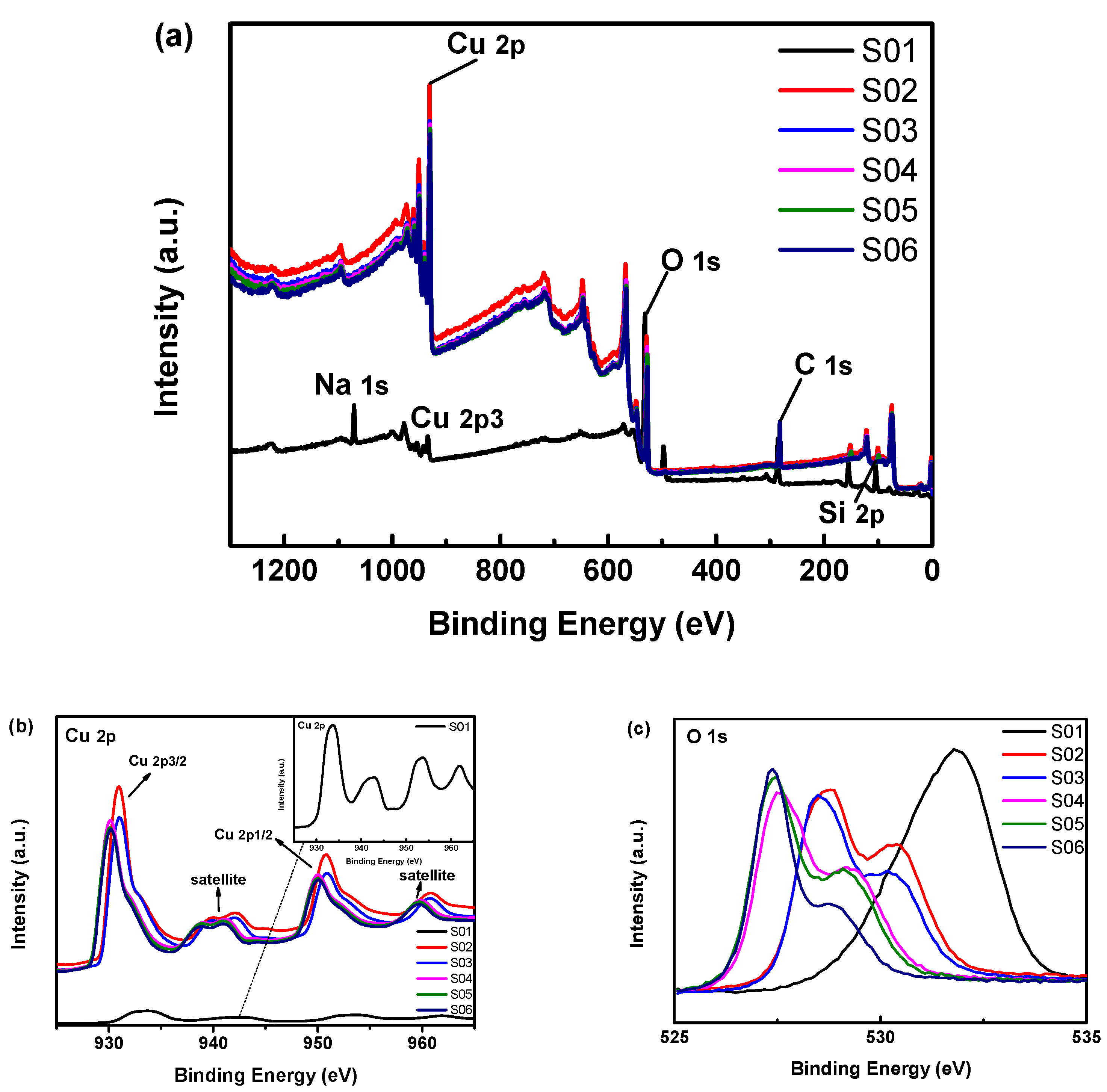
3.2. Compositional Properties of Cu2O Thin Films

As shown in Figure 5, the XPS spectra of Cu2O thin films deposited at various oxygen flow rates (S01 to S06) were analyzed to determine the chemical states of copper and oxygen. Figure 5a shows the full survey scan of all samples (S01 to S06), identifying the main elements present, including Cu, O, Na, C, and Si. Figure 5b focuses on the Cu 2p region of each sample, which is crucial for identifying the copper oxidation state. Figure 5b indeed displays satellite peaks around the Cu 2p region, which are typically indicative of the presence of Cu2+ species. The observation of these satellite peaks, including those with no or lower oxygen flow rates (such as S01 and S02), suggests that Cu2+ is present in varying degrees across all samples [21,22]. Figure 5c represents the O 1s region for each sample, which helps understand the oxygen chemical state and bonding. In the Cu 2p spectra, all samples exhibit prominent peaks around 933 eV and 953 eV, corresponding to the Cu 2p3/2 and Cu 2p1/2 binding energies, respectively [23]. The S01 sample, deposited with only argon gas, exhibits the relatively lowest intensity among all samples. As the oxygen flow rate increases, starting from the S02 sample, a significant increase in the intensity of the Cu 2p peaks is observed. The S02 sample, which has the lowest oxygen concentration among the oxygenated samples, shows the highest peak intensity. This suggests an increased presence of Cu ions due to the additional Cu plasma scattering [24]. However, as the oxygen concentration continues to increase from S03 to S06, a gradual decrease in the peak intensity of Cu 2p is observed. This decrease indicates a reduction in the surface concentration of Cu ions, likely due to the formation of more oxidized copper species (such as CuO or Cu4O3), which alter the surface chemistry [25]. The O 1s spectrum in Figure 5c also reveals a similar trend. For the S01 sample, the peak intensity is significantly lower compared to the oxygenated samples. As the oxygen flow rate increases in the S02 sample, the binding energy of O 1s decreases, indicating a shift in the chemical environment of oxygen atoms. The peak intensity of O 1s in the S02 sample is the highest among all samples. From S03 to S06, as the oxygen concentration further increases, the O 1s peak intensity decreases. This trend suggests a saturation point where additional oxygen does not significantly increase the oxygen content on the surface but may lead to the formation of more complex oxides, such as Cu4O3, as indicated by the XRD analysis.

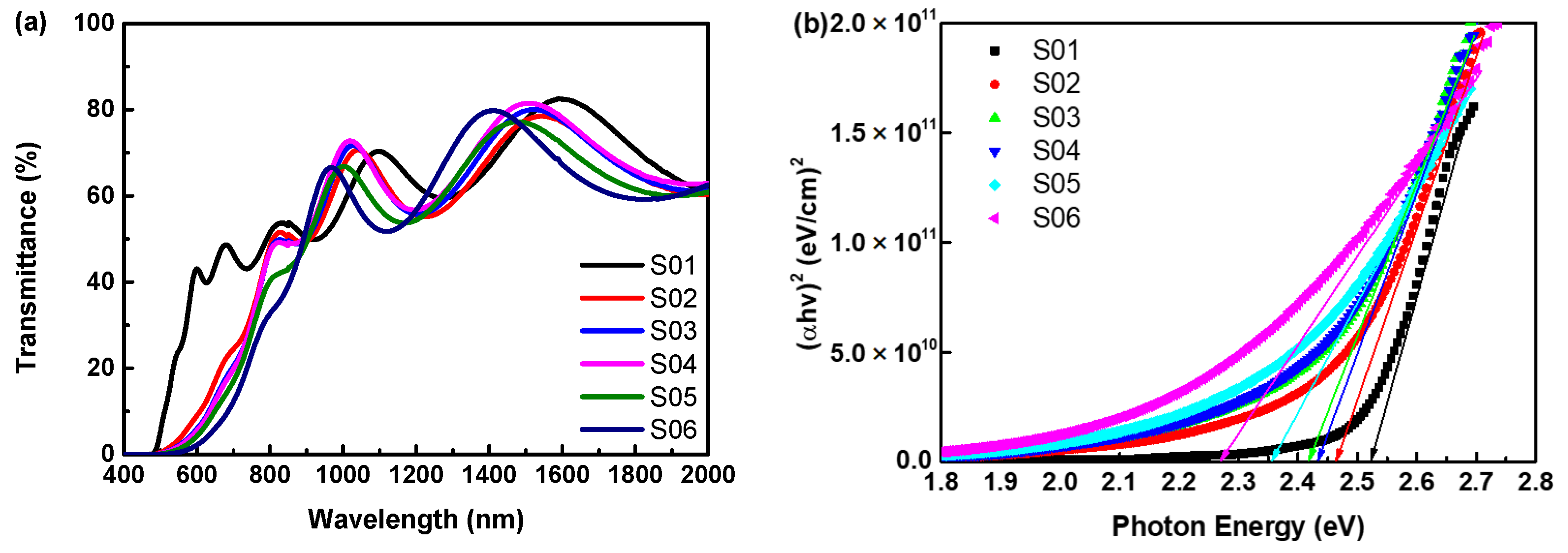
3.3. Optical Properties of Cu2O Thin Films

Figure 6 presents the UV-Vis-NIR spectroscopy results, showcasing the transmittance spectra and the optical band gap energies of Cu2O thin films deposited at various oxygen flow rates. The transmittance range of all samples in Figure 6a is approximately 400 nm to 2000 nm. The S01 sample deposited with argon gas alone exhibits the highest transmittance of 57% across the entire wavelength range. As the oxygen flow rate increases from S02 to S06, an overall decrease is observed in the transmittance of each sample, varying from 52% to 49%. This trend suggests that higher oxygen content in the deposition environment leads to films with reduced optical transparency. The transmittance spectra display several characteristic peaks and valleys, indicating interference effects and possible electronic transitions within the films. These features shift to the right with increasing oxygen flow rates, reflecting changes in film thickness, surface morphology, crystallographic, and compositional properties.
Figure 6b shows the optical band gap energy (Eg) of Cu2O thin films with variations in oxygen flow rates. The Eg was determined by applying Tauc’s plot, which extrapolates the linear portion of the (αhν)2 versus plot to the photon energy axis (x-axis) [26]. The intercept gives the value of the Eg. The S01 sample deposited with only argon gas shows the highest Eg, approximately 2.52 eV. This value is in good consistency with the typical band gap energy of Cu2O thin films [27]. As the oxygen flow rate further increased, the Eg of the Cu2O films decreased from 2.46 eV at S02 to 2.26 eV at S06. The trend in decreasing band gap energy with higher oxygen flow rates correlates well with the transmittance data, where higher oxygen content leads to films with poorer optical properties and lower transparency. This reduction in band gap indicates that the crystallinity of the Cu2O thin films deteriorates and the defect density and impurities increase [28]. These results align well with the structural and surface analyses provided by XRD and SEM, further confirming the critical role of oxygen in tailoring the properties of Cu2O thin films.

4. Conclusions

In this study, we systematically investigated the influence of varying oxygen flow rates on the structural, morphological, compositional, and optical properties of Cu2O thin films deposited by RF magnetron sputtering. Our comprehensive analysis through XRD, FE-SEM, XPS, and UV-Vis-NIR spectroscopy provides several key insights into the behavior of Cu2O films under different deposition conditions. XRD analysis confirmed that the crystal structure of the Cu2O films transitioned significantly with the introduction of oxygen. Initially, pure Cu2O films exhibited a cubic crystal structure. As the oxygen content increased, we observed the coexistence of Cu2O and CuO phases, eventually leading to the formation of a Cu4O3 tetragonal structure in the S06 sample. This phase transformation, accompanied by changes in diffraction peak intensities and positions, underscores the pivotal role of oxygen in dictating the crystallographic properties of the films. FE-SEM analysis revealed distinct changes in surface morphology and film density with varying oxygen flow rates. Higher oxygen content resulted in finer grain formation and more compact films up to S04, while further increasing the oxygen flow led to larger, less uniform grains, indicating phase transitions and altered growth mechanisms. The observed morphological evolution is consistent with the structural changes identified through XRD. XPS analysis highlighted the impact of oxygen flow on the chemical states of copper and oxygen in the films. The Cu 2p and O 1s spectra showed that increasing oxygen content initially enhanced the presence of Cu ions. This compositional shift aligns with the phase transformations observed in XRD. UV-Vis-NIR spectroscopy results demonstrated that increasing oxygen content reduced the optical transmittance and band gap energy of the Cu2O films. The highest transmittance and band gap energy was observed in the S01 sample deposited with only argon gas. As the oxygen flow rate increased, the transmittance decreased, and the band gap energy reduced, indicating a deterioration in crystallinity and an increase in defect density and impurities. These findings collectively emphasize the importance of oxygen flow rate control in tailoring the properties of Cu2O thin films. The ability to manipulate the structural, morphological, compositional, and optical characteristics through precise oxygen flow adjustments offers valuable insights for optimizing these films for specific electronic and optical applications. Future work could explore the detailed mechanisms behind the observed phase transformations and their impact on the functional properties of Cu2O-based devices, paving the way for enhanced performance in practical applications.

Author Contributions

Conceptualization, J.P. and D.H.; methodology, Y.-G.S. and C.-S.S.; validation, J.P. and D.H.; formal analysis, J.P. and Y.-G.S.; investigation, J.P. and D.H.; resources, C.-S.S. and D.H.; data curation, J.P.; writing—original draft preparation, J.P.; writing—review and editing, Y.-G.S. and D.H.; visualization, J.P. and D.H.; supervision, C.-S.S. and D.H.; project administration, D.H.; funding acquisition, C.-S.S. and D.H. All authors have read and agreed to the published version of the manuscript.

Funding

This work was supported by the National Research Foundation of Korea (NRF) grant funded by the Korean government (MSIT) (No. NRF-2018R1A5A1025594) and was supported by “Regional Innovation Strategy (RIS)” through the National Research Foundation of Korea (NRF) funded by the Ministry of Education (MOE) (No. 2023RIS-007).

Institutional Review Board Statement

Not applicable.

Informed Consent Statement

Not applicable.

Data Availability Statement

Data are contained within the article.

Conflicts of Interest

The authors declare no conflicts of interest.

References

  1. Jo, J.; Lenef, J.D.; Mashooq, K.; Trejo, O.; Dasgupta, N.P.; Peterson, R.L. Causes of the Difference between Hall Mobility and Field-Effect Mobility for p-Type RF Sputtered Cu2O Thin-Film Transistors. IEEE Trans. Electron. Devices 2020, 67, 5557–5563. [Google Scholar] [CrossRef]
  2. Sun, S.; Zhang, X.; Yang, Q.; Liang, S.; Zhang, X.; Yang, Z. Cuprous oxide (Cu2O) crystals with tailored architectures: A comprehensive review on synthesis, fundamental properties, functional modifications and applications. Prog. Mater. Sci. 2018, 96, 111–173. [Google Scholar] [CrossRef]
  3. Houng, B.; Wu, J.K.; Yeh, P.C.; Yeh, W.L.; Sun, C.K. Effect of Cu addition on the properties of the RF magnetron-sputtered Cu2O thin films. J. Electroceram. 2021, 45, 129–134. [Google Scholar] [CrossRef]
  4. Kardarian, K.; Nunes, D.; Maria Sberna, P.; Ginsburg, A.; Keller, D.A.; Vaz Pinto, J.; Deuermeier, J.; Anderson, A.Y.; Zaban, A.; Martins, R.; et al. Effect of Mg doping on Cu2O thin films and their behavior on the TiO2/Cu2O heterojunction solar cells. Sol. Energy Mater. Sol. Cells 2016, 147, 27–36. [Google Scholar] [CrossRef]
  5. Дёмин В, Г.; Brungardt, M.V.; Goncharova, E.A.; Fedorov, L.Y.; Karpov, I.V.; Ushakov, A.V. Investigation of the effect of oxygen partial pressure on the phase composition of copper oxide nanoparticles by vacuum arc synthesis. Tech. Phys. 2022, 67, 2410. [Google Scholar]
  6. Al-Kuhaili, M.F. Characterization of copper oxide thin films deposited by the thermal evaporation of cuprous oxide (Cu2O). Vacuum 2008, 82, 623–629. [Google Scholar] [CrossRef]
  7. Ungeheuer, K.; Marszalek, K.W.; Mitura-Nowak, M.; Jelen, P.; Perzanowski, M.; Marszalek, M.; Sitarz, M. Cuprous Oxide Thin Films Implanted with Chromium Ions-Optical and Physical Properties Studies. Int. J. Mol. Sci. 2022, 23, 8358. [Google Scholar] [CrossRef]
  8. Liau, L.C.-K.; Tang, C.-H. Effect of a Cu2O buffer layer on the efficiency in p-Cu2O/ZnO hetero-junction photovoltaics using electrochemical deposition processing. J. Appl. Electrochem. 2022, 52, 1459–1467. [Google Scholar] [CrossRef]
  9. Patwary, M.A.M.; Saito, K.; Guo, Q.; Tanaka, T. Influence of oxygen flow rate and substrate positions on properties of Cu-oxide thin films fabricated by radio frequency magnetron sputtering using pure Cu target. Thin Solid. Films 2019, 675, 59–65. [Google Scholar] [CrossRef]
  10. Reddy, A.S.; Uthanna, S.; Reddy, P.S. Properties of dc magnetron sputtered Cu2O films prepared at different sputtering pressures. Appl. Surf. Sci. 2007, 253, 5287–5292. [Google Scholar] [CrossRef]
  11. Dolai, S.; Dey, R.; Das, S.; Hussain, S.; Bhar, R.; Pal, A.K. Cupric oxide (CuO) thin films prepared by reactive d.c. magnetron sputtering technique for photovoltaic application. J. Alloys Compd. 2017, 724, 456–464. [Google Scholar] [CrossRef]
  12. Wee, S.H.; Huang, P.S.; Lee, J.K.; Goyal, A. Heteroepitaxial Cu2O thin film solar cell on metallic substrates. Sci. Rep. 2015, 5, 16272. [Google Scholar] [CrossRef] [PubMed]
  13. Kim, H.-S.; Kumar, M.D.; Park, W.-H.; Patel, M.; Kim, J. Cu4O3-based all metal oxides for transparent photodetectors. Sens. Actuators A Phys. 2017, 253, 35–40. [Google Scholar] [CrossRef]
  14. Patwary, M.A.M.; Ho, C.Y.; Saito, K.; Guo, Q.; Yu, K.M.; Walukiewicz, W.; Tanaka, T. Effect of oxygen flow rate on properties of Cu4O3 thin films fabricated by radio frequency magnetron sputtering. J. Appl. Phys. 2020, 127, 085302. [Google Scholar] [CrossRef]
  15. Patwary, M.A.M.; Saito, K.; Guo, Q.; Tanaka, T.; Man Yu, K.; Walukiewicz, W. Nitrogen Doping Effect in Cu4O3 Thin Films Fabricated by Radio Frequency Magnetron Sputtering. Phys. Status Solidi (b) 2019, 257, 1900363. [Google Scholar] [CrossRef]
  16. Cruz Almazán, M.A.; Vigueras Santiago, E.; López, R.; Hernández López, S.; Castrejón Sánchez, V.H.; Esparza, A.; Encarnación Gómez, C. Cu4O3 thin films deposited by non-reactive rf-magnetron sputtering from a copper oxide target. Rev. Mex. De Física 2021, 67, 495–499. [Google Scholar]
  17. Rahmat, R.; Heryanto, H.; Ilyas, S.; Fahri, A.N.; Mutmainna, I.; Rahmi, M.H.; Tahir, D. The relation between structural, optical, and electronic properties of composite CuO/ZnO in supporting photocatalytic performance. Desalination Water Treat. 2022, 270, 289–301. [Google Scholar] [CrossRef]
  18. Purusottam-Reddy, B.; Sivajee-Ganesh, K.; Jayanth-Babu, K.; Hussain, O.M.; Julien, C.M. Microstructure and supercapacitive properties of rf-sputtered copper oxide thin films: Influence of O2/Ar ratio. Ionics 2015, 21, 2319–2328. [Google Scholar] [CrossRef]
  19. Solache-Carranco, H.; Juarez-Diaz, G.; Galvan-Arellano, M.; Martinez-Juarez, J.; Romero-Paredes, R.G.; Pena-Sierra, R. Raman scattering and photoluminescence studies on Cu2O. In Proceedings of the 5th International Conference on Electrical Engineering, Computing Science and Automatic Control, Mexico City, Mexico, 12–14 November 2008. [Google Scholar]
  20. Jagadish, K.A.; Kekuda, D. Thermal annealing effect on phase evolution, physical properties of DC sputtered copper oxide thin films and transport behavior of ITO/CuO/Al Schottky diodes. Appl. Phys. A Mater. Sci. Process 2024, 130, 315. [Google Scholar] [CrossRef]
  21. Hsu, Y.-K.; Yu, C.-H.; Chen, Y.-C.; Lin, Y.-G. Synthesis of novel Cu2O micro/nanostructural photocathode for solar water splitting. Electrochim. Acta 2013, 105, 62–68. [Google Scholar] [CrossRef]
  22. Pawar, S.M.; Kim, J.; Inamdar, A.I.; Woo, H.; Jo, Y.; Pawar, B.S.; Cho, S.; Kim, H.; Im, H. Multi-functional reactivelysputtered copper oxide electrodes for supercapacitor and electrocatalyst in direct methanol fuel cell applications. Sci. Rep. 2016, 6, 21310. [Google Scholar] [CrossRef] [PubMed]
  23. Luo, L.; Kang, Y.; Yang, J.C.; Zhou, G. Effect of oxygen gas pressure on orientations of Cu2O nuclei during the initial oxidation of Cu(100), (110) and (111). Surf. Sci. 2012, 606, 1790–1797. [Google Scholar] [CrossRef]
  24. Ghodselahi, T.; Vesaghi, M.A.; Shafiekhani, A.; Baghizadeh, A.; Lameii, M. XPS study of the Cu@Cu2O core-shell nanoparticles. Appl. Surf. Sci. 2008, 255, 2730–2734. [Google Scholar] [CrossRef]
  25. Poulston, S.; Parlett, P.M.; Stone, P.; Bowker, M. Surface Oxidation and Reduction of CuO and Cu2O Studied Using XPS and XAES. Surf. Interface Anal. 1998, 24, 811–820. [Google Scholar] [CrossRef]
  26. Messaoudi, O.; Assaker, I.B.; Gannouni, M.; Souissi, A.; Makhlouf, H.; Bardaoui, A.; Chtourou, R. Structural, morphological and electrical characteristics of electrodeposited Cu2O: Effect of deposition time. Appl. Surf. Sci. 2016, 366, 383–388. [Google Scholar] [CrossRef]
  27. Wang, Y.; Miska, P.; Pilloud, D.; Horwat, D.; Mücklich, F.; Pierson, J.F. Transmittance enhancement and optical band gap widening of Cu2O thin films after air annealing. J. Appl. Phys. 2014, 115, 073505. [Google Scholar] [CrossRef]
  28. Alajlani, Y.; Placido, F.; Barlow, A.; Chu, H.O.; Song, S.; Ur Rahman, S.; De Bold, R.; Gibson, D. Characterisation of Cu2O, Cu4O3, and CuO mixed phase thin films produced by microwave-activated reactive sputtering. Vacuum 2017, 144, 217–228. [Google Scholar] [CrossRef]
Figure 1. XRD patterns of Cu2O thin films deposited at various oxygen flow rates.
Coatings 14 00930 g001
Figure 2. FWHM and crystallite size of Cu2O thin films as a function of oxygen flow rate.
Coatings 14 00930 g002
Figure 3. Raman spectra of Cu2O thin films deposited at various oxygen flow rates.
Coatings 14 00930 g003
Figure 4. Surface and cross-sectional FE-SEM images of Cu2O thin films deposited at various oxygen flow rates.
Coatings 14 00930 g004
Figure 5. XPS spectra of Cu2O thin films deposited at various oxygen flow rates: (a) the full survey scan of all samples (S01 to S06), (b) Cu 2p region for each sample, and (c) O 1s region for each sample.
Coatings 14 00930 g005
Figure 6. UV-Vis-NIR spectroscopy results of Cu2O thin films deposited at various oxygen flow rates: (a) the transmittance spectra and (b) the optical band gap.
Coatings 14 00930 g006
Disclaimer/Publisher’s Note: The statements, opinions and data contained in all publications are solely those of the individual author(s) and contributor(s) and not of MDPI and/or the editor(s). MDPI and/or the editor(s) disclaim responsibility for any injury to people or property resulting from any ideas, methods, instructions or products referred to in the content.

