
Self-Assembled Pd Nanocomposites into a Monolayer for Enhanced Sensing Performance

Abstract
:1. Introduction
2. Materials and Methods
2.1. Synthesis Process
2.2. Surface Characterization
2.3. SERS Experiment
2.4. Simulation Conditions
Principle of Extinction Properties
2.5. XRD Analysis
3. Results and Discussion
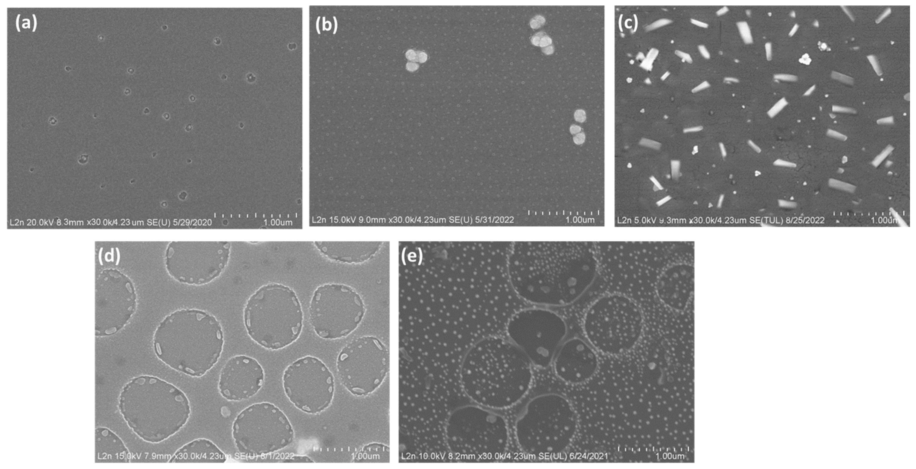
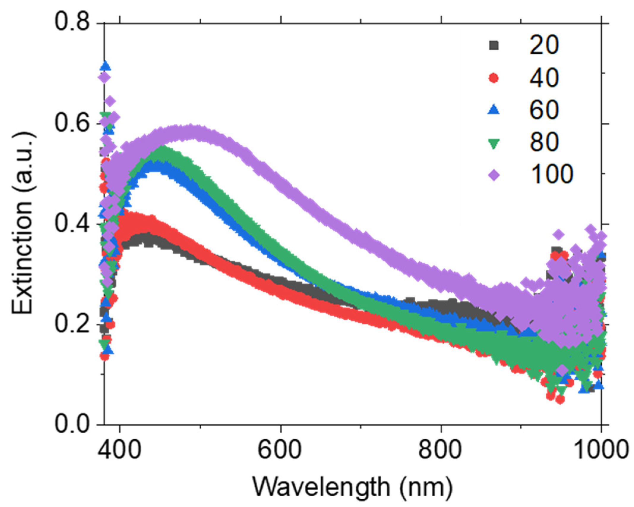
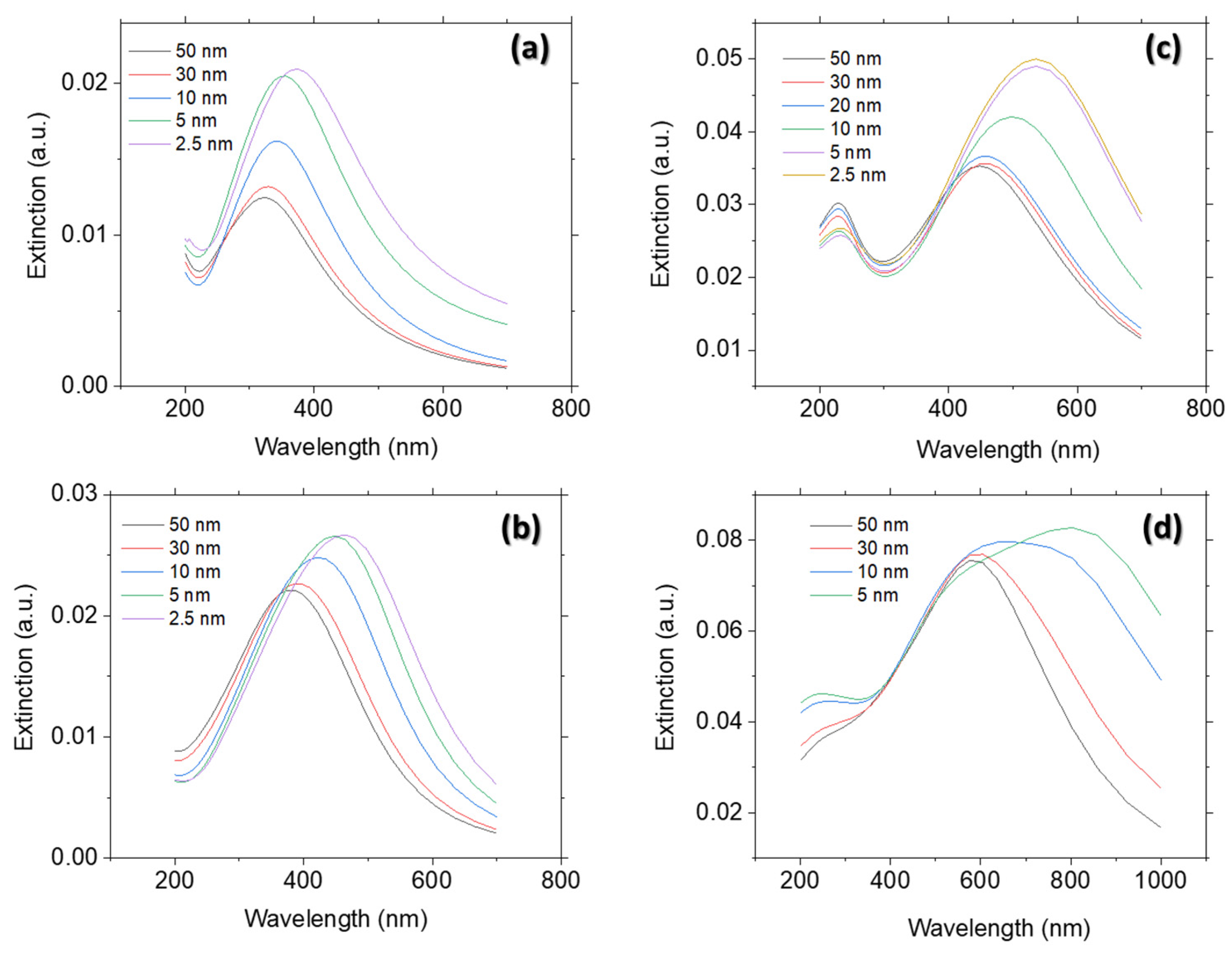
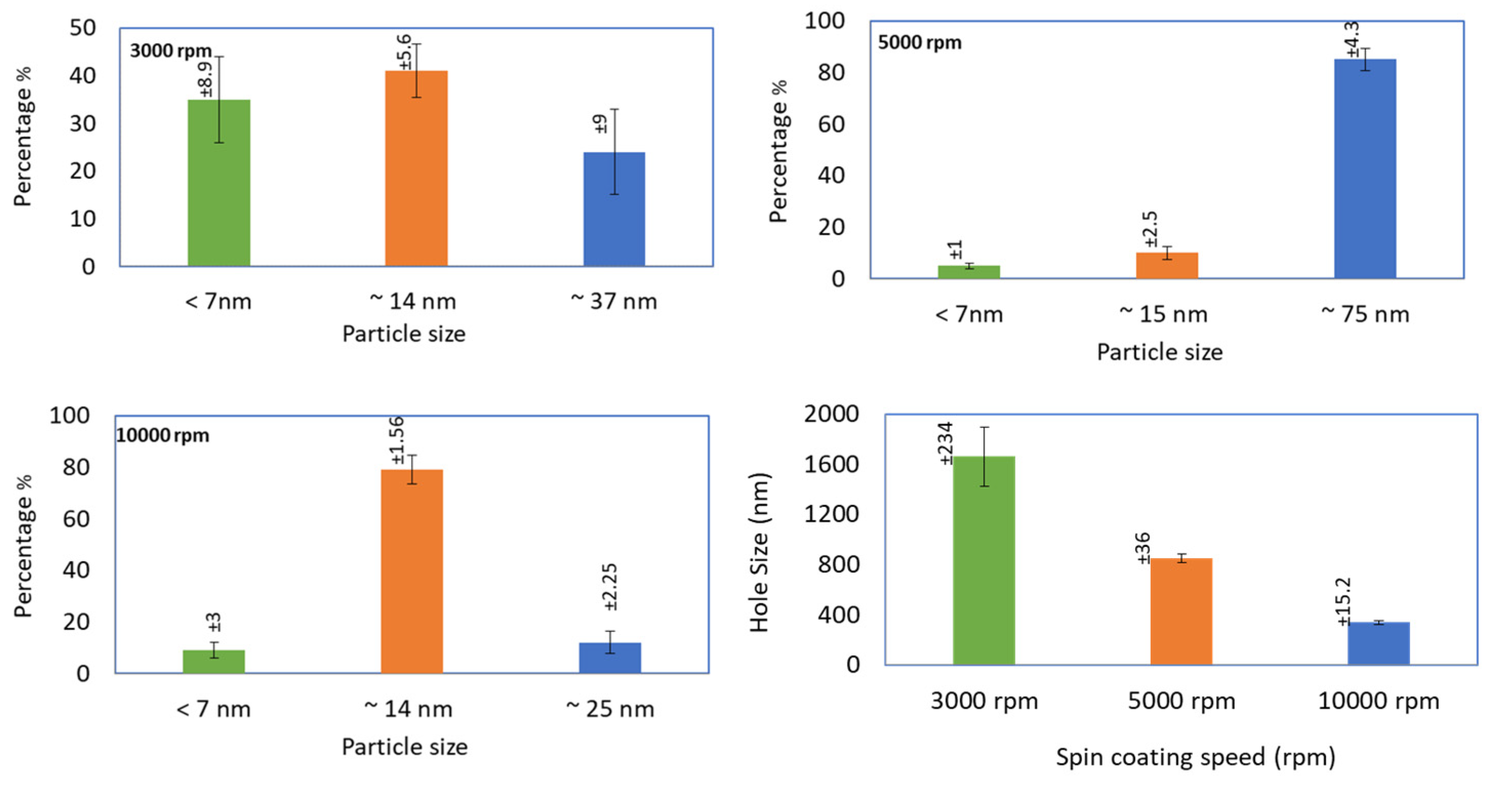
3.1. Adjusting Pd Precursor Concentration
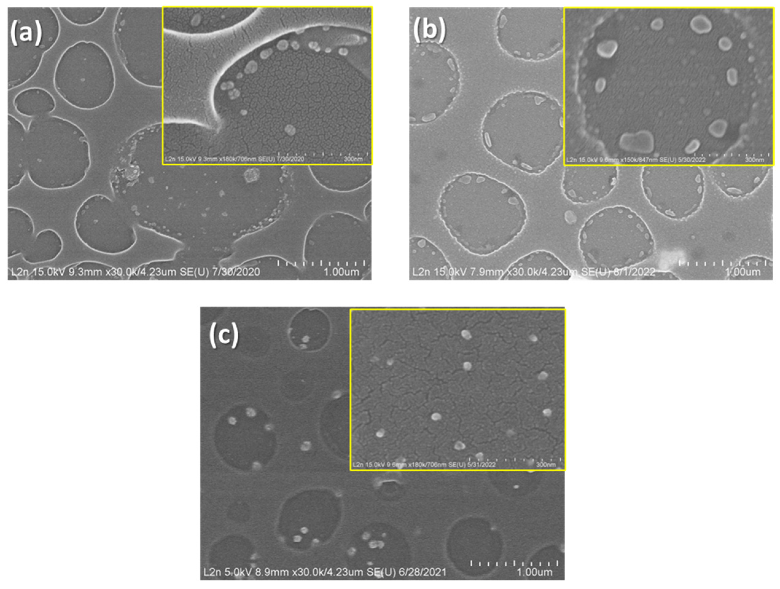
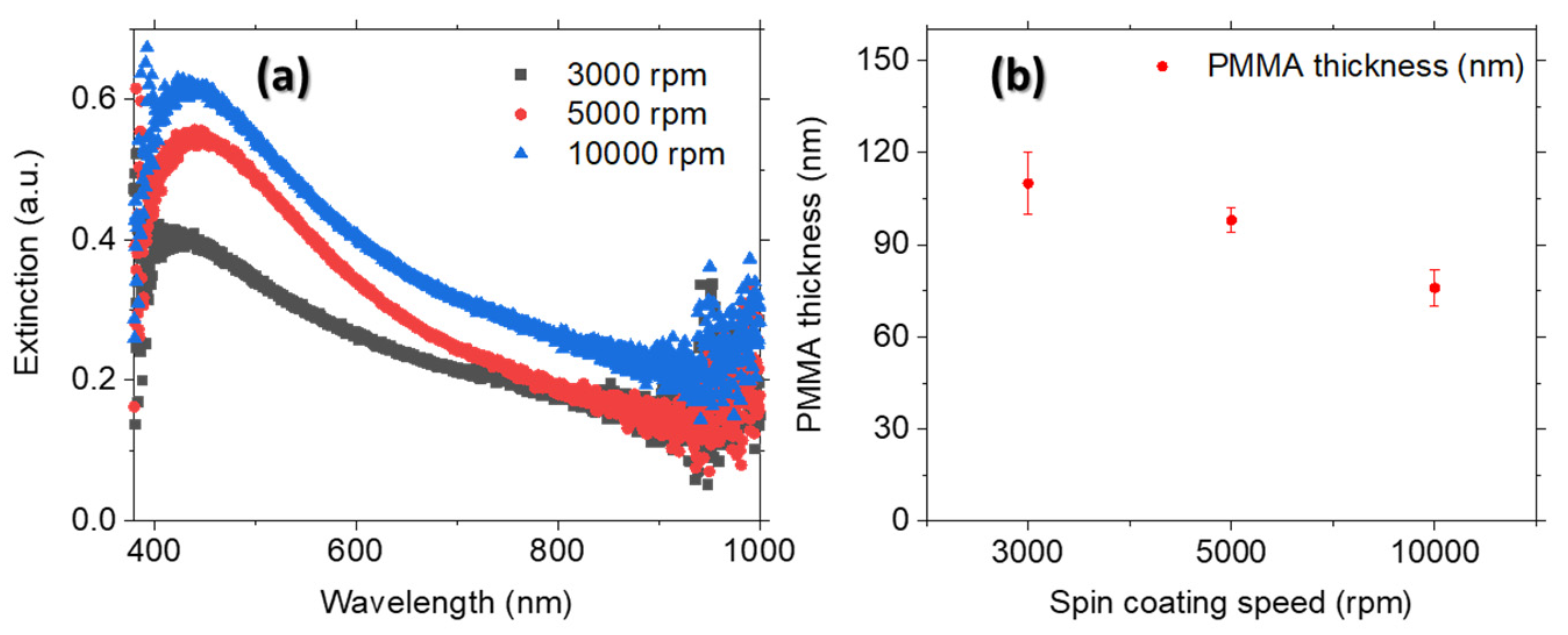
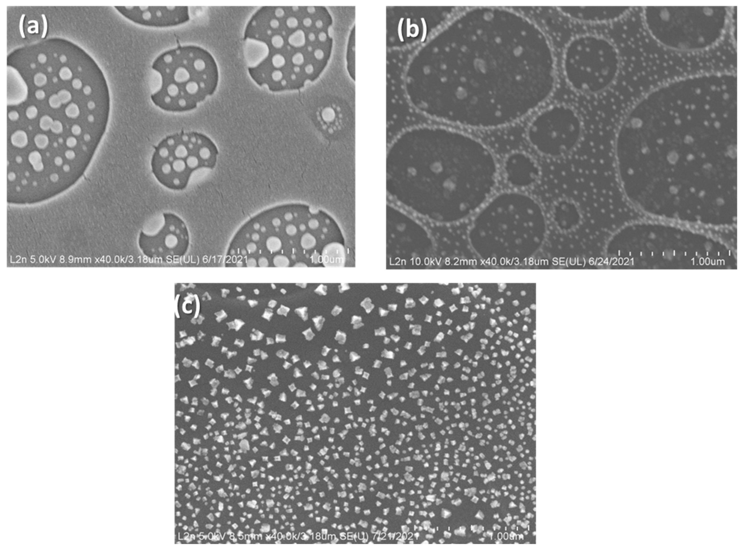
3.2. Solvent Evaporation Rate (ER) Mediated PdNPs Synthesis at High Precursor Concentrations
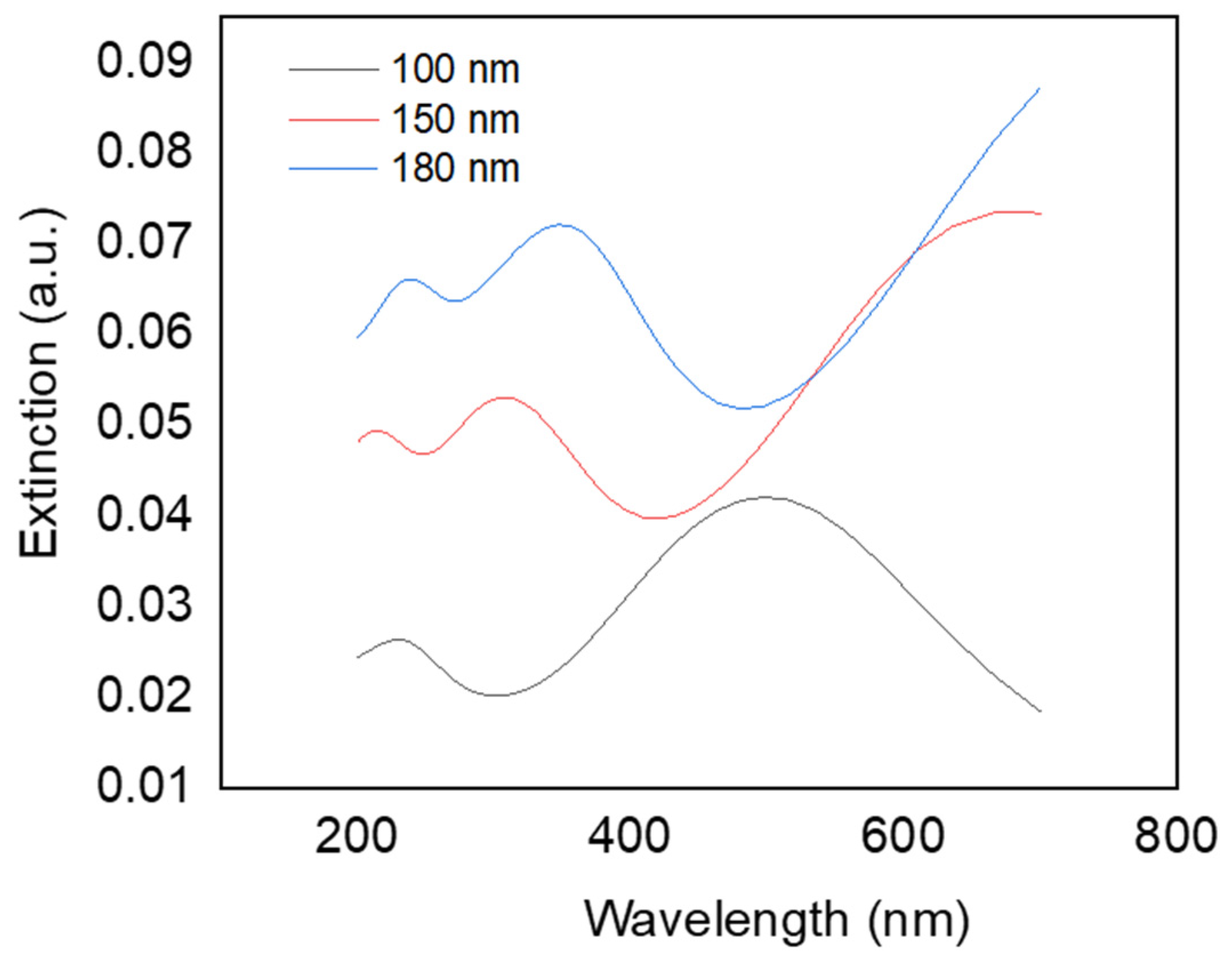
3.3. SERS Performance
4. Conclusions
Author Contributions
Funding
Institutional Review Board Statement
Informed Consent Statement
Data Availability Statement
Conflicts of Interest
References
- Fan, H.; Yang, K.; Boye, D.M.; Sigmon, T.; Malloy, K.J.; Xu, H.; López, G.P.; Brinker, C.J. Self-assembly of ordered, robust, three-dimensional gold nanocrystal/silica arrays. Science 2004, 304, 567–571. [Google Scholar] [CrossRef] [PubMed]
- Collier, C.; Vossmeyer, T.; Heath, A.J. Nanocrystal superlattices. Annu. Rev. Phys. Chem. 1998, 49, 371–404. [Google Scholar] [CrossRef] [PubMed]
- Rechberger, W.; Hohenau, A.; Leitner, A.; Krenn, J.; Lamprecht, B.; Aussenegg, F. Optical properties of two interacting gold nanoparticles. Opt. Commun. 2003, 220, 137–141. [Google Scholar] [CrossRef]
- Gunnarsson, L.; Rindzevicius, T.; Prikulis, J.; Kasemo, B.; Käll, M.; Zou, S.; Schatz, G.C. Confined plasmons in nanofabricated single silver particle pairs: Experimental observations of strong interparticle interactions. J. Phys. Chem. B 2005, 109, 1079–1087. [Google Scholar] [CrossRef] [PubMed]
- Jain, P.K.; Huang, W.; El-Sayed, M.A. On the universal scaling behavior of the distance decay of plasmon coupling in metal nanoparticle pairs: A plasmon ruler equation. Nano Lett. 2007, 7, 2080–2088. [Google Scholar] [CrossRef]
- Su, K.-H.; Wei, Q.-H.; Zhang, X.; Mock, J.; Smith, D.R.; Schultz, S. Interparticle coupling effects on plasmon resonances of nanogold particles. Nano Lett. 2003, 3, 1087–1090. [Google Scholar] [CrossRef]
- Koenderink, A.F.; de Waele, R.; Prangsma, J.C.; Polman, A. Experimental evidence for large dynamic effects on the plasmon dispersion of subwavelength metal nanoparticle waveguides. Phys. Rev. B 2007, 76, 201403. [Google Scholar] [CrossRef]
- Zou, S.; Schatz, G.C. Narrow plasmonic/photonic extinction and scattering line shapes for one and two dimensional silver nanoparticle arrays. J. Chem. Phys. 2004, 121, 12606–12612. [Google Scholar] [CrossRef] [PubMed]
- Elghanian, R.; Storhoff, J.J.; Mucic, R.C.; Letsinger, R.L.; Mirkin, C.A. Selective colorimetric detection of polynucleotides based on the distance-dependent optical properties of gold nanoparticles. Science 1997, 277, 1078–1081. [Google Scholar] [CrossRef] [PubMed]
- Sonnichsen, C.; Reinhard, B.M.; Liphardt, J.; Alivisatos, A.P. A molecular ruler based on plasmon coupling of single gold and silver nanoparticles. Nat. Biotechnol. 2005, 23, 741–745. [Google Scholar] [CrossRef]
- Warburton, R.J.; Schäflein, C.; Haft, D.; Bickel, F.; Lorke, A.; Karrai, K.; Garcia, J.M.; Schoenfeld, W.; Petroff, P.M. Optical emission from a charge-tunable quantum ring. Nature 2000, 405, 926–929. [Google Scholar] [CrossRef] [PubMed]
- Rabaud, W.; Saminadayar, L.; Mailly, D.; Hasselbach, K.; Benoit, A.; Etienne, B. Persistent currents in mesoscopic connected rings. Phys. Rev. Lett. 2001, 86, 3124. [Google Scholar] [CrossRef] [PubMed]
- Mailly, D.; Chapelier, C.; Benoit, A. Experimental observation of persistent currents in GaAs-AlGaAs single loop. Phys. Rev. Lett. 1993, 70, 2020. [Google Scholar] [CrossRef] [PubMed]
- Nielsch, K.; Wehrspohn, R.; Barthel, J.; Kirschner, J.; Gösele, U.; Fischer, S.; Kronmüller, H. Hexagonally ordered 100 nm period nickel nanowire arrays. Appl. Phys. Lett. 2001, 79, 1360–1362. [Google Scholar] [CrossRef]
- Winzer, M.; Kleiber, M.; Dix, N.; Wiesendanger, R. Fabrication of nano-dot-and nano-ring-arrays by nanosphere lithography. Appl. Phys. Rev. 1996, 63, 617–619. [Google Scholar] [CrossRef]
- Liu, S.-D.; Yang, Z.; Liu, R.-P.; Li, X.-Y. High sensitivity localized surface plasmon resonance sensing using a double split nanoring cavity. J. Phys. Chem. C 2011, 115, 24469–24477. [Google Scholar] [CrossRef]
- Jiang, H.; Sabarinathan, J. Effects of coherent interactions on the sensing characteristics of near-infrared gold nanorings. J. Phys. Chem. C 2010, 114, 15243–15250. [Google Scholar] [CrossRef]
- Sun, S.; Zeng, H.; Robinson, D.B.; Raoux, S.; Rice, P.M.; Wang, S.X.; Li, G. Monodisperse MFe2O4 (M = Fe, Co, Mn) nanoparticles. J. Am. Chem. Soc. 2004, 126, 273–279. [Google Scholar] [CrossRef] [PubMed]
- Kim, M.W.; Ku, P.-C. The metal-clad semiconductor nanoring laser and its scaling properties. Opt. Express 2011, 19, 3218–3225. [Google Scholar] [CrossRef]
- Castano, F.; Ross, C.; Frandsen, C.; Eilez, A.; Gil, D.; Smith, H.I.; Redjdal, M.; Humphrey, F. Metastable states in magnetic nanorings. Phys. Rev. B 2003, 67, 184425. [Google Scholar] [CrossRef]
- Wu, C.; Zhu, H.; Dai, J.; Yan, W.; Yang, J.; Tian, Y.; Wei, S.; Xie, Y. Room-Temperature Ferromagnetic Silver Vanadium Oxide (Ag1.2V3O8): A Magnetic Semiconductor Nanoring Structure. Adv. Funct. Mater. 2010, 20, 3666–3672. [Google Scholar] [CrossRef]
- Wen, Z.; Wei, H.; Han, X. Patterned nanoring magnetic tunnel junctions. Appl. Phys. Lett. 2007, 91, 122511. [Google Scholar] [CrossRef]
- Xia, Y.; Yang, P.; Sun, Y.; Wu, Y.; Mayers, B.; Gates, B.; Yin, Y.; Kim, F.; Yan, H. One-dimensional nanostructures: Synthesis, characterization, and applications. Adv. Mater. 2003, 15, 353–389. [Google Scholar] [CrossRef]
- Möller, M.; Spatz, J.P.; Roescher, A. Gold nanoparticles in micellar poly (styrene)-b-poly (ethylene oxide) films—Size and interparticle distance control in monoparticulate films. Adv. Mater. 1996, 8, 337–340. [Google Scholar] [CrossRef]
- Zhang, J.; Liu, Y.; Ke, Y.; Yan, H. Periodic square-like gold nanoparticle arrays templated by self-assembled 2D DNA nanogrids on a surface. Nano Lett. 2006, 6, 248–251. [Google Scholar] [CrossRef] [PubMed]
- Sharma, J.; Chhabra, R.; Liu, Y.; Ke, Y.; Yan, H. DNA-templated self-assembly of two-dimensional and periodical gold nanoparticle arrays. Angew. Chem. 2006, 118, 744–749. [Google Scholar] [CrossRef]
- Li, M.; Zhang, H.; Zhang, J.; Wang, C.; Han, K.; Yang, B. Easy preparation and characterization of highly fluorescent polymer composite microspheres from aqueous CdTe nanocrystals. J. Colloid. Interface Sci. 2006, 300, 564–568. [Google Scholar] [CrossRef] [PubMed]
- Chehadi, Z.; Alkees, N.; Bruyant, A.; Toufaily, J.; Girardon, J.-S.; Capron, M.; Dumeignil, F.; Hamieh, T.; Bachelot, R.; Jradi, S. Plasmonic enhanced photocatalytic activity of semiconductors for the degradation of organic pollutants under visible light. Mater. Sci. Semicond. Process. 2016, 42, 81–84. [Google Scholar] [CrossRef]
- Jiang, N.; Zhuo, X.; Wang, J. Active plasmonics: Principles, structures, and applications. Chem. Rev. 2017, 118, 3054–3099. [Google Scholar] [CrossRef]
- Li, J.F.; Huang, Y.F.; Ding, Y.; Yang, Z.L.; Li, S.B.; Zhou, X.S.; Fan, F.R.; Zhang, W.; Zhou, Z.Y.; Wu, D.Y.; et al. Shell-isolated nanoparticle-enhanced Raman spectroscopy. Nature 2010, 464, 392–395. [Google Scholar] [CrossRef]
- Li, L.; Hutter, T.; Steiner, U.; Mahajan, S. Single molecule SERS and detection of biomolecules with a single gold nanoparticle on a mirror junction. Analyst 2013, 138, 4574–4578. [Google Scholar] [CrossRef] [PubMed]
- Khanafer, M.; Issa, A.; Akil, S.; Hamieh, T.; Adam, P.-M.; Jradi, S. A general strategy to incorporate a wide range of metallic salts into ring-like organized nanostructures via polymer self-assembly. RSC Adv. 2016, 6, 102843–102852. [Google Scholar] [CrossRef]
- Omar, R.; Naciri, A.E.; Jradi, S.; Battie, Y.; Toufaily, J.; Mortada, H.; Akil, S. One-step synthesis of a monolayer of monodisperse gold nanocubes for SERS substrates. J. Mater. Chem. C 2017, 5, 10813–10821. [Google Scholar] [CrossRef]
- Kralchevsky, P.; Denkov, N.; Paunov, V.; Velev, O.; Ivanov, I.; Yoshimura, H.; Nagayama, K. Formation of two-dimensional colloid crystals in liquid films under the action of capillary forces. J. Condens. Matter Phys. 1994, 6, A395. [Google Scholar] [CrossRef]
- Zhang, L.; Bai, Y.; Shang, Z.; Zhang, Y.; Mo, Y. Experimental and theoretical studies of Raman spectroscopy on 4-mercaptopyridine aqueous solution and 4-mercaptopyridine/Ag complex system. J. Raman Spectrosc. 2007, 38, 1106–1111. [Google Scholar] [CrossRef]
- Khanafer, M.; Izquierdo-Lorenzo, I.; Akil, S.; Louarn, G.; Toufaily, J.; Hamieh, T.; Adam, P.M.; Jradi, S. Silver Nanoparticle Rings of Controllable Size: Multi-Wavelength SERS Response and High Enhancement of Three Pyridine Derivatives. ChemistrySelect 2016, 1, 1201–1206. [Google Scholar] [CrossRef]
- Fahes, A.; En Naciri, A.; Navvabpour, M.; Jradi, S.; Akil, S. Self-assembled Ag nanocomposites into ultra-sensitive and reproducible large-area SERS-Active opaque substrates. Nanomaterials 2021, 11, 2055. [Google Scholar] [CrossRef] [PubMed]
- Omar, R.; Naciri, A.E.; Fahes, A.; Jradi, S.; Issa, A.; Kuznetsov, D.; Shur, V.; Zelenovskiy, P.; Battie, Y.; Akil, S. Precise control of the size and gap between gold nanocubes by surface-based synthesis for high SERS performance. Soft Matter 2020, 16, 1857–1865. [Google Scholar] [CrossRef] [PubMed]
- Akil, S.; Omar, R.; Kuznetsov, D.; Shur, V.; En Naciri, A.; Jradi, S. Advanced Large-Scale Nanofabrication Route for Ultrasensitive SERS Platforms Based on Precisely Shaped Gold Nanostructures. Nanomaterials 2021, 11, 1806. [Google Scholar] [CrossRef] [PubMed]
- Fahes, A.; Naciri, A.E.; Shoker, M.B.; Akil, S. Self-assembly-based integration of Ag@Au oligomers and core/shell nanoparticles on polymer chips for efficient sensing devices. Soft Matter 2023, 19, 321–330. [Google Scholar] [CrossRef]
- Yu, Y.; Zhao, Y.; Huang, T.; Liu, H. Shape-controlled synthesis of palladium nanocrystals by microwave irradiation. Pure Appl. Chem. 2009, 81, 2377–2385. [Google Scholar] [CrossRef]
- Yin, J.; Zhang, L.; Jiao, T.; Zou, G.; Bai, Z.; Chen, Y.; Zhang, Q.; Xia, M.; Peng, Q. Highly efficient catalytic performances of nitro compounds and morin via self-assembled MXene-Pd nanocomposites synthesized through self-reduction strategy. Nanomaterials 2019, 9, 1009. [Google Scholar] [CrossRef] [PubMed]


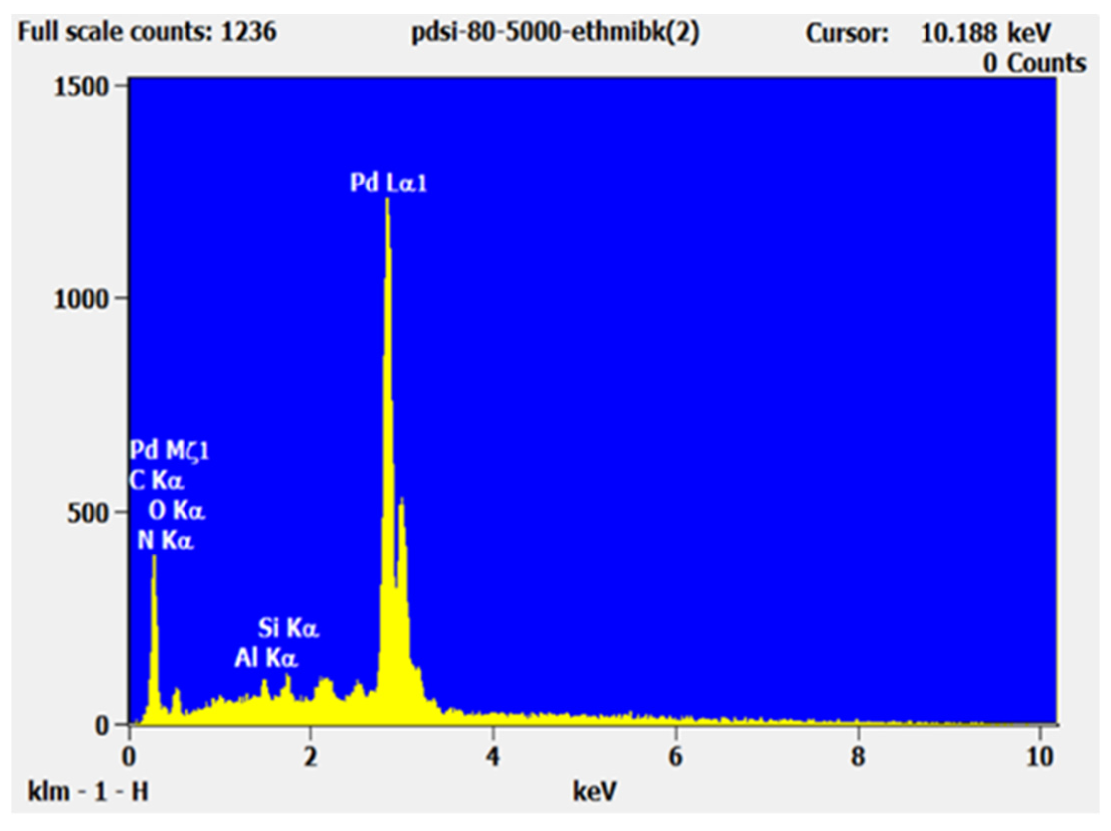
| Element Line | Net Counts | Weight % | Weight Error | Atom% | Atom % Error | Formula |
|---|---|---|---|---|---|---|
| C K | 423 | 5.7 | 0.23 | 20.6 | 1.8 | C |
| N K | 35 | 1.9 | 1.2 | 6 | 7.2 | N |
| O K | 151 | 6.5 | 0.7 | 17.7 | 4 | O |
| Si K | 1693 | 18.1 | 0.4 | 28 | 1.2 | Si |
| Pd L | 2294 | 67.7 | 2.2 | 27.6 | 1.8 | Pd |
| Total | 100 | 100 | ||||
| C K | 423 | 5.7 | 0.2 | 20.6 | 1.8 | C |
| Spin Coating Speed (rpm) | LSPR Band (nm) | ISERS/INORMAL |
|---|---|---|
| 3000 | 440 | 20 |
| 5000 | 465 | 25 |
| 10,000 | 455 | 33 |
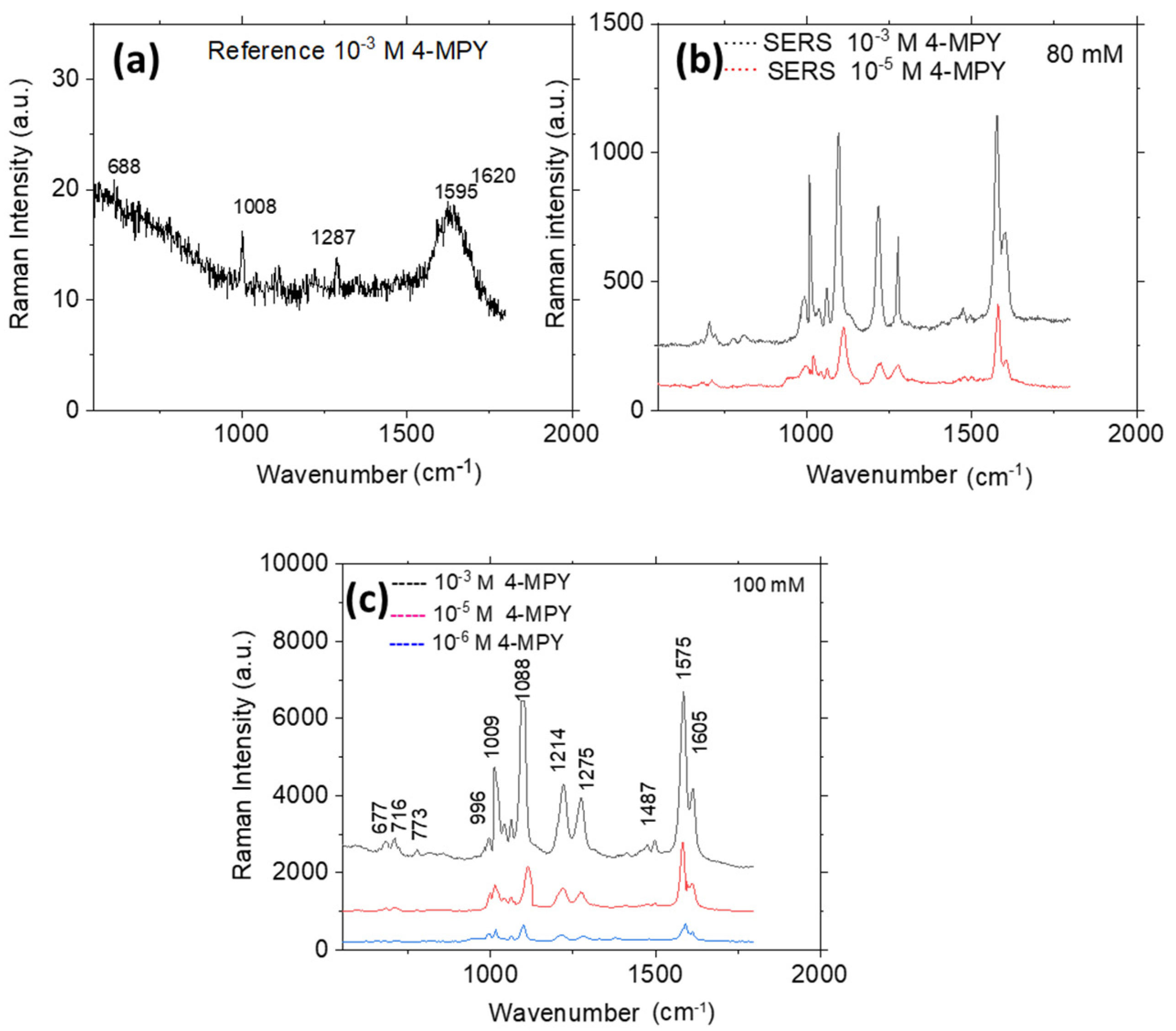
| Raman | SERS | Plane | Assignment |
|---|---|---|---|
429 645 688 721 781 1003 1042 1053 1117 1215 1225 1252 1287 1467 1488 1500 1595 1620 Str = stretching; bend = bending; def = deformation; wag = wagging; Sciss = scissoring; breath = breathing. | 425 677 701 716 773 812 996 1009 1032 1051 1088 1214 1275 1450 1487 1575 1605 | Out Out Out In Out In Out Out Out Out Out Out In In In In In Out In In In In In In In In In | Wag C2H8, C5H10 Wag C1H7, C4H9 Wag N-H Str R Def R, wag N-H Str R, str C-S Def C-H Wag C1H7, C2H8 Wag C4H9, C5H10 Def N-H+ Wag C-H Wag C-H Ring breath Trigonal ring breath Def R, bend C-H, N-H Trigonal ring breath, str C-S Sciss C-H Bend C-H Sciss C-H Bend C1H7, C5H10, N-H Def R, bend C-H Bend C-H in the same direction Trigonal ring breath, be C-H Def R, bend C-H, N-H, str C-N Wag C-H Str C@C with deprotonated nitrogen Str C@C with protonated nitrogen |
Disclaimer/Publisher’s Note: The statements, opinions and data contained in all publications are solely those of the individual author(s) and contributor(s) and not of MDPI and/or the editor(s). MDPI and/or the editor(s) disclaim responsibility for any injury to people or property resulting from any ideas, methods, instructions or products referred to in the content. |
© 2024 by the authors. Licensee MDPI, Basel, Switzerland. This article is an open access article distributed under the terms and conditions of the Creative Commons Attribution (CC BY) license (https://creativecommons.org/licenses/by/4.0/).
Share and Cite
Navvabpour, M.; Adam, P.-M.; Jradi, S.; Akil, S. Self-Assembled Pd Nanocomposites into a Monolayer for Enhanced Sensing Performance. Coatings 2024, 14, 934. https://doi.org/10.3390/coatings14080934
Navvabpour M, Adam P-M, Jradi S, Akil S. Self-Assembled Pd Nanocomposites into a Monolayer for Enhanced Sensing Performance. Coatings. 2024; 14(8):934. https://doi.org/10.3390/coatings14080934
Chicago/Turabian StyleNavvabpour, Mohammad, Pierre-Michel Adam, Safi Jradi, and Suzanna Akil. 2024. "Self-Assembled Pd Nanocomposites into a Monolayer for Enhanced Sensing Performance" Coatings 14, no. 8: 934. https://doi.org/10.3390/coatings14080934