Abstract
Phototransistors are three-terminal photodetectors that usually have a higher photocurrent gain than photodiodes due to the amplification of the gate electrode. In this work, a broad spectral phototransistor based on copper phthalocyanine (CuPc) and a Cs3Bi2I9 (CBI) heterojunction is fabricated by the full vacuum evaporation method. Due to the complementary UV–visible absorption of CuPc and CBI, the device exhibits superior performance under three different types of visible light illumination. The experimental results show that the structure of the organic/perovskite heterojunction active layer has the characteristics of good compatibility and a simple process. Meanwhile, by utilizing the superior light-absorption characteristics of perovskite materials and the strong exciton dissociation efficiency of a hetero-type heterojunction interface, the CuPc/CBI-PT exhibits a higher photoresponsivity, photosensitivity, specific detection rate, and lower operating voltage than the CuPc reference device. The stability test shows that the CuPc/CBI-PT can still obtain a 0.73 A/W photoresponsivity under 660 nm light illumination after being stored in the air for 360 h without any packaging. This indicates that the organic/perovskite heterojunction PT may be a good choice for the preparation of high-performance photodetectors.
1. Introduction
Photodetectors can be divided into ultraviolet [1,2], visible [3], and infrared detectors [4,5] according to the different working wavelengths, which are widely used in many fields such as civil and military. Among these, broad spectral visible light detectors are suitable as receivers for visible light wireless communication systems and have many applications in future artificial intelligence scenarios such as smart homes, smart cities, and the Internet of Things [6,7]. In the image sensor, the most important component is the photodetector with high sensitivity, whose performance determines the imaging quality of the image sensor [8]. Photodetectors mainly include photodiodes [9] and photosensitive field-effect transistors (phototransistors, PTs) [2,5,10]. Among these photodetectors, the PTs can magnify the photocurrent by its transconductance and also have the function of optical signal switching and optical signal amplifying. It has a high gain and good signal-to-noise ratio and has broad application prospects [5,11].
The PT has a structure similar to that of a thin-film transistor (TFT), consisting of three electrodes (gate, source, and drain), a gate insulation layer, and an active layer. The difference between the PT and TFT is that the functional layer is made of photosensitive materials, so the device not only has the traditional field-effect characteristics but also the channel current will be significantly amplified under light illumination due to the photoconduction and photovoltaic effects [12,13]. Since the first PT was reported [14], after more than 20 years of research on PTs, a series of high-performance inorganic compounds [15], organic small molecules [16], polymers [17], quantum dots [18], and perovskite [19] photosensitive materials have been synthesized. A variety of PTs using planar heterojunctions [20], bulk heterojunctions [21], hybrid heterojunctions [22], and vertical structures [23] have been reported, and the performances of PTs have been greatly improved.
Copper phthalocyanine (CuPc) is a common organic small-molecule-conjugated photosensitive material with high hole mobility, a high absorption coefficient to visible light, and good stability. There are many reports on CuPc-based PTs [10,24]. In addition, perovskite is a type of high-performance photoelectric material that has been extensively studied in recent years. Perovskite not only has a high absorption coefficient, high carrier mobility, and long luminous life but also has a long diffusion length, which has been widely used in solar cells [25], light-emitting diodes [26], sensors [27], and lasers [28]. Zou et al. reported a vertical PT composed of a single-crystalline MAPbBr3 perovskite, which exhibits excellent photoresponse performance with a photoresponsivity (R) of 16 A/W and a high detectivity of 1014 Jones [29]. Sun et al. reported CH3NH3PbI3-based FETs, which show a high R of 1 A/W and photosensitivity of 18000%, respectively [30]. In contrast, all-inorganic halide perovskite has better stability because it uses inorganic components to replace the organic functional groups in organic–inorganic perovskite. Cs3Bi2I9 (CBI) is an all-inorganic halide perovskite-like material where Cs3+ replaces organic groups, and Bi2+ substitutes for Pb2+, thus making it more environmentally friendly. In this paper, combining the advantages of the above two functional materials, PTs based on a CuPc/CBI planar heterojunction (CuPc/CBI-PT) are proposed, and all functional layers of PTs in this work are prepared by using the vacuum evaporation method [31,32].
Compared with the CuPc single-layer reference devices (CuPc-PT) and visible photodetectors reported in the recent literature [33,34,35,36], the optical detection performances of CuPc/CBI-PT for visible light have been significantly improved, which are mainly due to the efficient light absorption of 400–550 nm by CBI and the promotion of exciton dissociation by the CuPc/CBI heterojunction interface. The results show that the organic/perovskite heterojunction is a good choice for the preparation of phototransistors.
2. Materials and Methods
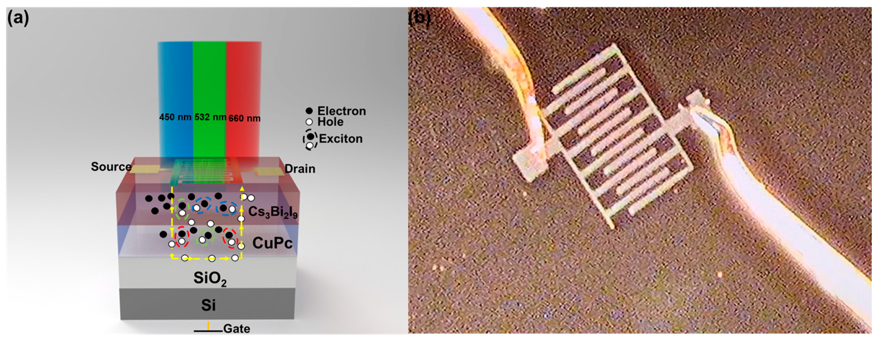
In this work, all devices adopt the structure of bottom-gate top-contact, as shown in Figure 1. A heavily doped n-type silicon (0.03 Ω·cm) was used as the substrate, and a 500 nm SiO2 layer was grown by the thermal oxidation method as the gate insulation layer. Cesium iodide (CsI, purity > 98%) was purchased from Xi’an Yuri Solar Co., LTD., and bismuth iodide (BiI3, purity > 98%) and copper phthalocyanine (CuPc, purity > 98%) were purchased from TCI (Shanghai) Development Co., Ltd. (Shanghai, China). After repeated ultrasonic cleaning with acetone, ethanol, and deionized water, the wafers were blown dry with N2 and placed in a plasma cleaner for 15 min before being immediately sent to the evaporation chamber. All functional layers were prepared by vacuum evaporation under 5×10⁻⁴ Pa. First, a 50 nm thick CuPc film was deposited on SiO2, and a 35 nm thick CBI layer was then prepared by alternating the evaporation of CsI and BiI3 at a certain thickness. The evaporation rate of the two materials was controlled at a 1:1.1 ratio by adjusting the evaporation power, which is monitored by a quartz crystal oscillator. Finally, 50 nm thick gold films were thermally evaporated as source/drain electrodes through a shadow mask with a channel length and width of 4800 µm and 25 µm and an effective channel area (A) of 12 mm2.

Figure 1.
(a) Schematic diagram of device structure and working principle; (b) photo of devices being tested.
The Detax XT surface profiler was used to measure the film’s thickness. X-ray diffraction (XRD) patterns of samples were obtained at room temperature using a Panaco Empyrean XRD instrument. The light absorptions of the samples were measured with the Shimazu UV 3600 Plus spectrophotometer. Lasers with wavelengths of 450 nm, 532 nm, and 660 nm were used as visible light sources, and dimmers with different transmittance were used to achieve different incident powers. The Agilent B1500A semiconductor device tester and Lakeshore TTPX vacuum probe station were used to test the photoelectric characteristics of the devices.
3. Results
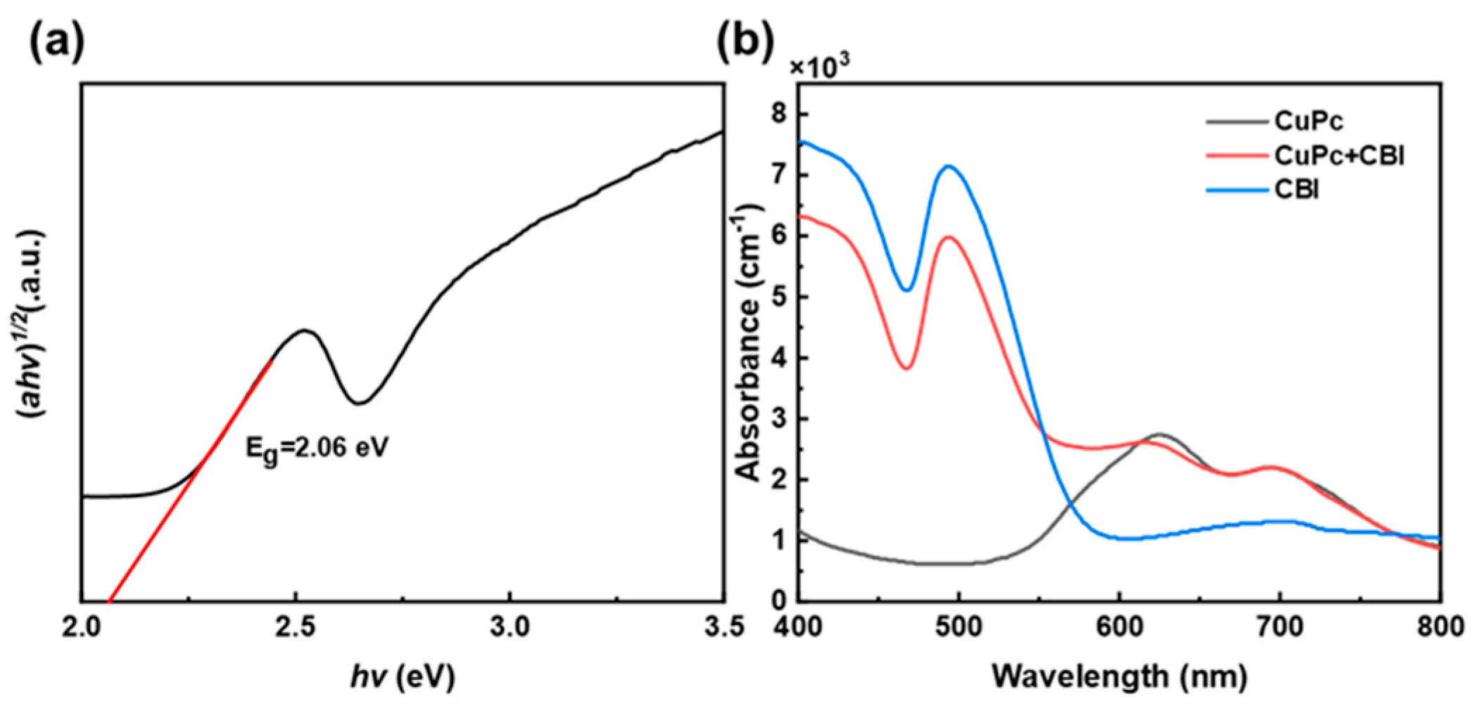
The band gap of the CBI was determined following the Tauc relation for an indirect band gap to plot hυ vs. (αhυ) 1/2 and to extrapolate the linear part to the x-axis, as Figure 2a illustrates [37].
where α is the absorption coefficient, hν is the photon energy, Eg is the optical band gap, and F is the fitting parameter. The band gap of the Cs3Bi2I9 film is 2.06 eV, which is consistent with the previous reports [38]. The band gap around 2 eV with a reasonable absorption coefficient is suitable for tandem solar cells and UV–Vis photodetectors.
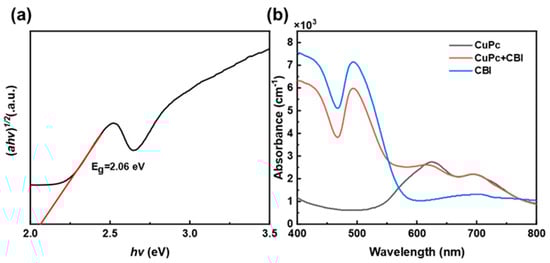
Figure 2.
(a) The hυ vs. (αhυ)1/2 relationship of CBI, and (b) the UV–VIS absorption spectra of thin films.
It can be seen from Figure 2b that the light absorption of CuPc and CBI is complementary in the visible range (400–780 nm), which is more conducive to the preparation of a wide spectrum of photodetectors.
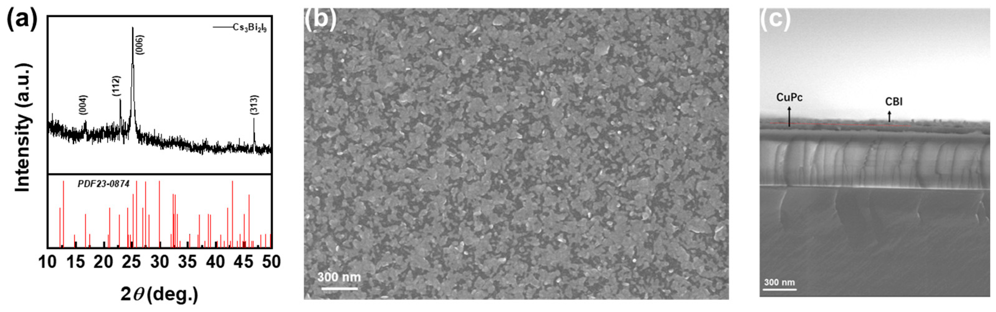
As shown in Figure 3a, the XRD pattern of the 35 nm Cs3Bi2I9 film deposited on a Si/SiO2 substrate by dual source co-evaporation shows that the diffraction peaks at 16.6°, 22.5°, 25.1°, and 46.2° are matched to the crystal faces of (004), (105), (006), and (209), respectively. It is consistent with the characteristic peak of the CBI reported in the various pieces of literature [39]. The diffraction peak of 2θ at 25.1° is the sharest, indicating that the sample has the highest growth degree in the preferred orientation of the (006) crystal plane and shows high crystallization. The surface SEM photo of the sample in Figure 3b shows that the CBI film prepared on the surface of CuPc is polycrystalline and uniform; the grain size of the CBI is about 30–50 nm. The cross-section SEM photo (Figure 3c) further shows a clear layered structure of the CuPc/CBI heterojunction.
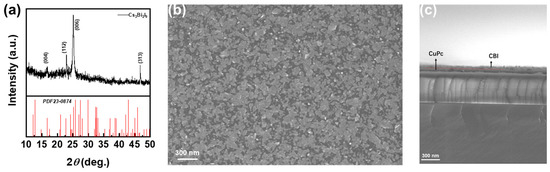
Figure 3.
(a) XRD pattern of Cs3Bi2I9 films prepared by evaporation. (b) Surface SEM photos of CuPc/CBI heterojunction films and (c) cross-section SEM photos of CuPc/CBI heterojunction films.
Figure 4a,b shows the output characteristics of the two devices under dark conditions. Compared with the CuPc-PT, the saturated output currents of the CuPc/CBI-PT are relatively smaller under the same bias conditions. In other words, the dark current of the heterojunction device was suppressed. In fact, according to the definition of photosensitivity (P) (Equation (2)), this may be beneficial for increasing the P of OPT.

Figure 4.
Output characteristics of (a) CuPc/CBI-PT and (b) CuPc-PT; (c) transfer characteristics of devices.
Figure 4c shows the transfer characteristics of the two devices under dark conditions. Obviously, the CuPc/CBI-PT has the lower dark currents.
According to the current–voltage equation of the field-effect transistor in the saturation region:
The calculated field-effect mobility of the CuPc/CBI-PT is 3.83 × 10⁻⁵ cm2/Vs, which is only 60% of the CuPc-PT (6.43 × 10⁻⁵ cm2/Vs). The CuPc-PT is a depletion-mode MOS, whose channel has been formed when at Vgs = 0 V, and the threshold voltage (Vth) is 11.98 V. Meanwhile, the Vth of the CuPc/CBI-PT moves towards the negative gate voltage, and it can be turned off at 3 V bias. This also provides low operating voltage conditions for achieving high P.
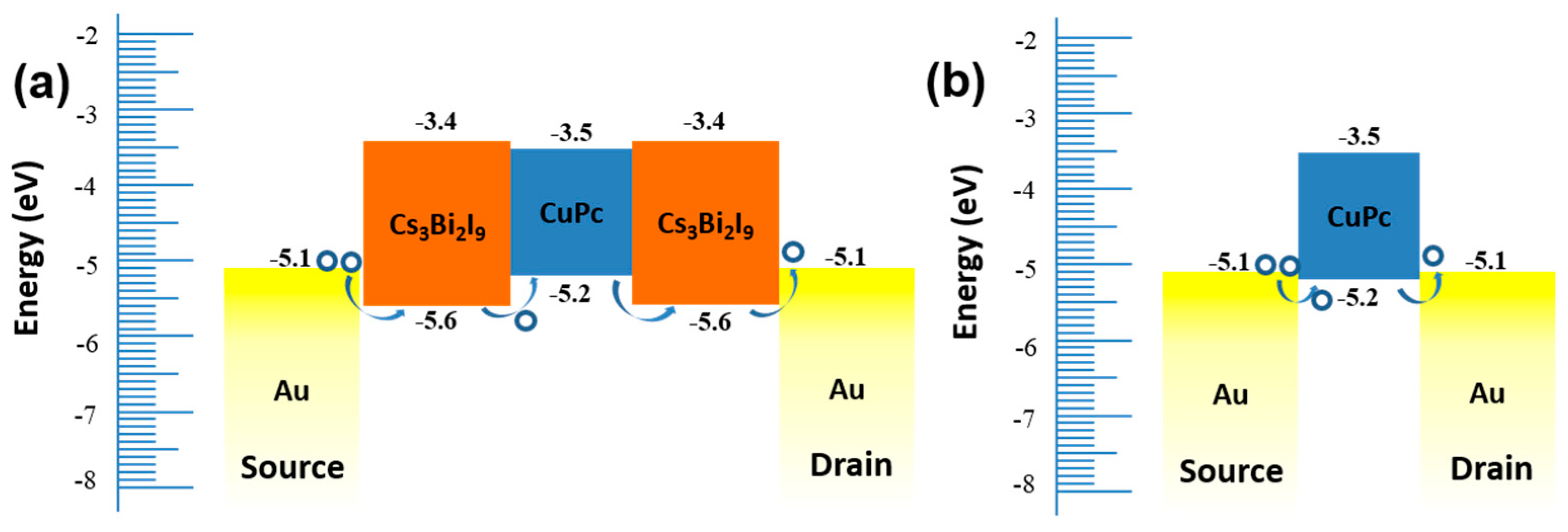
Figure 5 is a schematic diagram of the energy band in which carriers (holes) of the two devices are transported from the source to the drain. Due to the insertion of the CBI between the gold (Au) source/drain electrodes and CuPc in the CuPc/CBI-PT, there exists a large potential barrier (0.4–0.5 eV) for the injection of holes from the source electrode and the transmission from CuPc to CBI, which should be the main reason for suppressing the Idark and lowing down the opening voltage of the device.
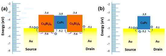
Figure 5.
Energy band diagrams of (a) CuPc/CBI-PT and (b) CuPc-PT.
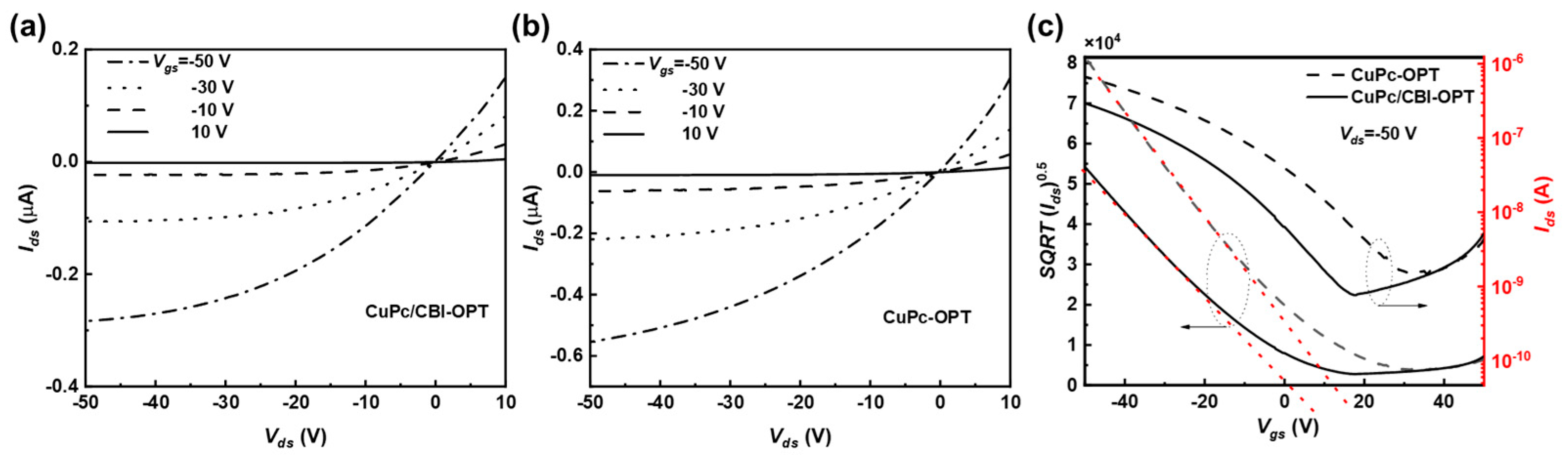
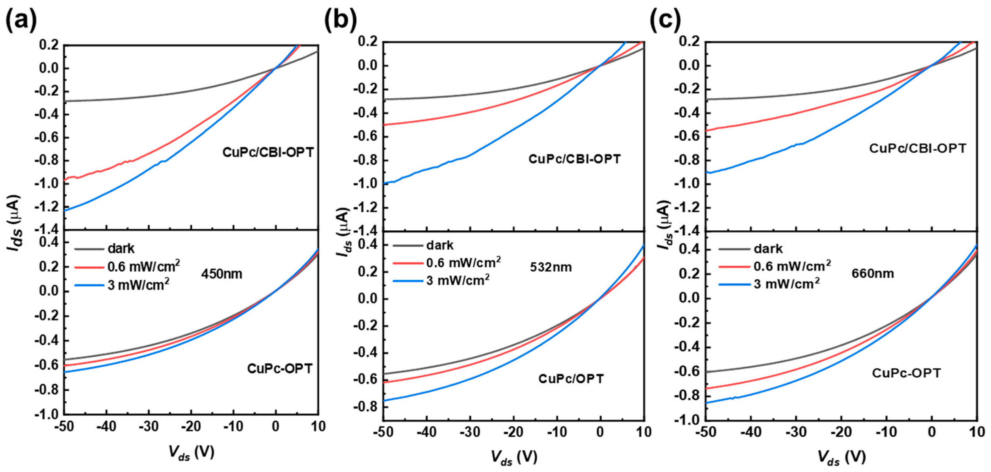
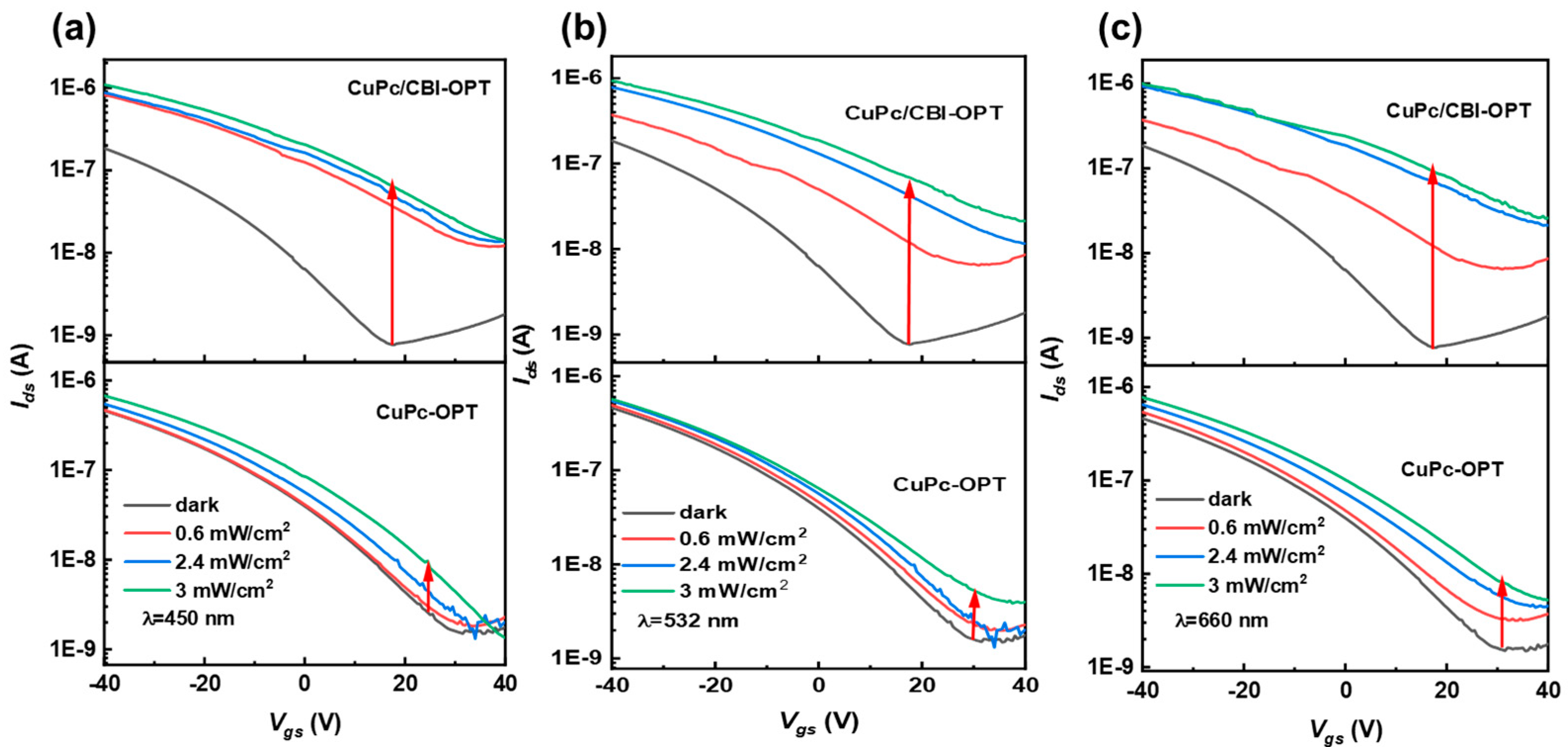
Figure 6 shows the light output characteristics of the two devices under different light illumination. In the bottom-gate top-contact structure PTs (Figure 1), light as the fourth “electrode” of the PT, in addition to gate, source, and drain, can play a similar role as the gate in regulating the output current of the PT [40]. As shown in Figure 6, under light illumination, whether 450 nm, 532 nm, or 660 nm, the CuPc/CBI-PT has more significant photosensitive characteristics than the CuPc-PT when Vgs = −50 V. In addition, the photocurrents of the CuPc/CBI-PT under 450 nm were greater than under 532 nm and 660 nm in the same bias conditions, which may be because the CuPc/CBI heterojunction film has a higher absorption coefficient at 450 nm. Conversely, the absorption of CuPc film under 450 nm is lower than that at 660 nm; thus, the CuPc-PT has a slightly better light response to 660 nm light illumination. (As shown in Figure 2b).
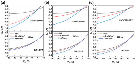
Figure 6.
Light output characteristics of the two devices under (a) 450 nm, (b) 532 nm, and (c) 660 nm light illumination (Vgs = −50 V).
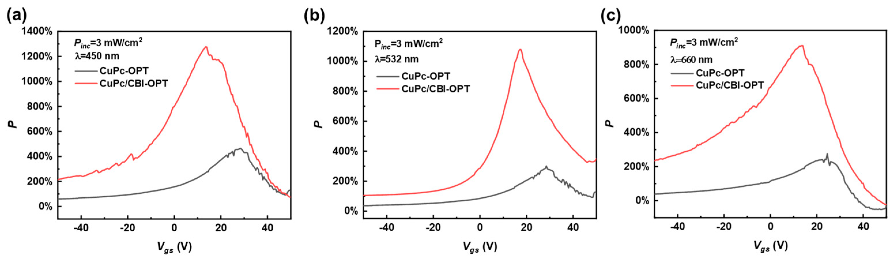
It can be seen from the red arrows of Figure 7 that the CuPc/CBI-PT has a significantly higher light/dark current ratio than the CuPc-PT. Further, by comparing the photosensitivity of the two devices at different gate voltages (as show in Figure 8), we can see that the Pmax of the CuPc/CBI-PT reaches 1277% @ Vgs = 13.5 V, while that of the CuPc-PT reaches 461% @ 28.0 V under 450 nm light illumination. The Pmax of the CuPc/CBI-PT reaches 1077% @ Vgs = 17.5 V, while that of the CuPc-PT reaches 300% @ 28.0 V under 532 nm light illumination. The Pmax of the CuPc/CBI-PT reaches 910% @ Vgs = 13.5 V, while that of the CuPc-PT reaches 277% @ 24.5 V under 660 nm light illumination. Obviously, the operating voltage of the CuPc/CBI-PT achieving the Pmax is also significantly smaller than that of the CuPc-PT. This indicates that the CuPc/CBI-PTs are able to operate at a lower bias voltage. As shown in Table 1, after illumination, the mobility of both devices is improved, which is attributed to the effect of reducing the electrode/active layer interface barrier caused by photogenerated carrier aggregation [41]. The mobility of CuPc/CBI-PT is ~3 times higher under light illumination than in the dark, while that of CuPc-PT is only 1.24–1.37 times. This shows that CuPc/CBI-PT has a better photogenerated carrier transport ability. Obviously, compared with CuPc-PT, the photoelectric performances of CuPc/CBI-PT have been greatly improved. We speculate that the reason is due to the photoinduced barrier-lowering effect in addition to the suppression of the dark current of the device by the interfacial barrier introduced by the inserted CBI between the Au source/drain and CuPc [41]. After illumination, the barrier height of the source/CBI interface and CBI/CuPc interface will be reduced, which will be more conducive to the transport of photogenerated carriers in heterojunction devices, thereby improving the photocurrent and further increasing the photosensitivity of the device.
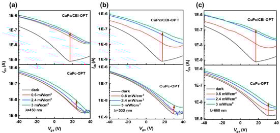
Figure 7.
Light transfer characteristics of the two devices under (a) 450 nm, (b) 532 nm, and (c) 660 nm light illumination (Vgs = −50 V).

Figure 8.
Relations between the photosensitivity and the gate voltage of the two devices under (a) 450 nm, (b) 532 nm, and (c) 660 nm light illumination.

Table 1.
The mobility of two devices under light and dark conditions.
The working principle of the CuPc/CBI-PT under light illumination is shown in Figure 1a, where the CBI and CuPc absorb the photons emitted by the light source at 450 nm, 532 nm, and 660 nm, respectively, to produce bound electron–hole pairs (excitons). According to the PT-related literature reports [21,42], excitons are more easily dissociated at positions with strong electric fields, such as the electrode/active layer and heterojunction interfaces. Under negative gate bias, the holes in the CuPc converge to the side close to SiO2 to form a channel. Both the photogenerated carriers and the carriers injected from the source should theoretically pass through the CBI to the CuPc channel layer. The photogenerated holes follow the route shown in Figure 1a, while the electrons are captured by defect states such as traps in the CuPc. The photogenerated holes participate in the transmission of the hole current in the channel and contribute to the drain output current under light illumination.
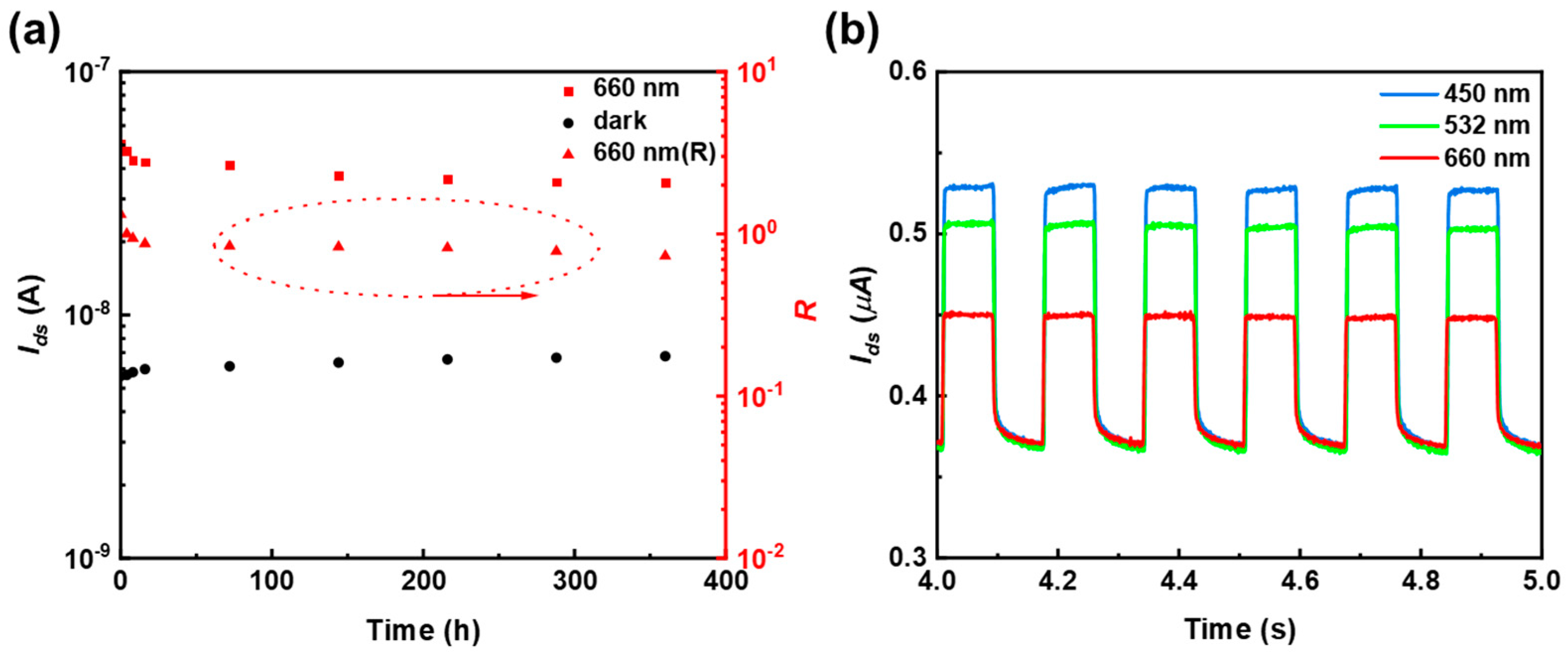
Finally, we monitored the stability of the CuPc/CBI-PTs for 360 h. As shown in Figure 9a, the dark current of the device increases from the initial 5.6 nA to 6.7 nA, and the photocurrent decays from the initial 50 nA to 35 nA under 660 nm light illumination. After the devices were stored in the air for 360 h (temperature 18–26 °C; humidity 40%–85%), the photoresponsivity (R) of the device still reached 0.73 A/W, which is 55% of the initial value, and tends to be stable, which indicates that the CuPc/CBI-PT has good stability. Photoresponsivity is defined as the ratio of the photocurrent (Iph) to the effective optical power received by the device channel [21,23]:
where Popt is the optical power density of the incident light.
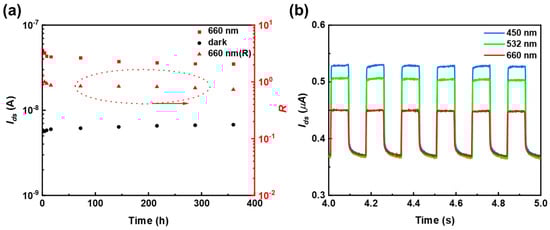
Figure 9.
(a) Stability testing of the CuPc/CBI-PT. (b) Current–time relationship under three different wavelength light illuminations.
Figure 9b shows the optical switching characteristics of the CuPc/CBI-PT device under three different wavelength light illuminations. The frequency of the chopper is 10 Hz. Under the conditions of 0.5 mW/cm2 and Vgs = Vds = −50 V, the device has the highest photocurrent gain under 450 nm illumination, medium under 532 nm illumination, and the lowest photocurrent gain under 660 nm illumination, which is consistent with the previous discussion on the light output characteristics (Figure 6). This is related to the absorption intensity of CuPc/CBI heterojunction films to different wavelengths of light (Figure 2b). According to Figure 9b, we can also obtain the response time of the CuPc/CBI-PT, which is about 3 ms at the rising edge and 7 ms at the falling edge. Finally, it can be seen from Table 2 that compared with the performance of visible light detectors reported in recent years, we believe that the maximum R and D* of the CuPc/CBI-PT have reached relatively high levels.
Table 2.
Performance parameters of visible PT in recent years.
4. Conclusions
In this work, a phototransistor based on a CuPc/CBI heterojunction was introduced. This device utilizes the complementary light-absorption characteristics of CuPc and CBI to achieve a wide optical spectrum response from UV to the visible region (−750 nm). By comparing with the reference device CuPc-PT, we find that the photoelectric performances of CuPc/CBI-PT were greatly improved. Through the analysis of the energy band and the working principle of devices, we speculate that the CuPc/CBI-PT has the following four advantages: 1. The complementary optical absorption bands of CuPc and CBI are used to increase the detection spectrum bandwidth of the device. 2. The high mobility of CuPc as a channel layer is suitable for carrier transport. 3. Interfacial barriers formed by the insertion of the CBI can effectively inhibit the dark current while the photocurrent is not affected, which is conducive to improving photoelectric performances. 4. The interfacial electric field of the heterojunction is beneficial to exciton dissociation and improves the exciton dissociation’s efficiency. At last, the CuPc/CBI-PT was stored in the air for 360 h without packaging, and its dark current only increased by 19.6%, and the photoresponsivity decreased by 45%, still reaching 0.73 A/W. This is still better than many visible light detectors reported in recent years [33,34,35,36] and even reaches a level similar to the current commercial α-si detectors (1 A/W). The results show that the CuPc/CBI-PT prepared by the full evaporation method provides a new choice for the realization of high-performance photodetectors with a simple process.
Author Contributions
Conceptualization, Y.W. and B.Y.; validation, Y.W., Y.C., X.Z. and B.J.; formal analysis, Y.W., X.Z. and B.J.; investigation, X.P. and B.Y.; resources, Q.Y. and B.Y.; data curation, Y.C.; writing—original draft preparation, Y.W.; writing—review and editing, X.P. and B.Y.; visualization, Y.W.; supervision, B.Y.; project administration, B.Y. All authors have read and agreed to the published version of the manuscript.
Funding
This work was supported by the Zhejiang Province Public Welfare Technology Application Research Project (Grant No. LGG21F050001) and the Science and Technology Planning Project of Shaoxing City (No. 2023B41006).
Institutional Review Board Statement
Not applicable.
Informed Consent Statement
Not applicable.
Data Availability Statement
Data are contained within the article.
Conflicts of Interest
Author Qing Yu was employed by the company United Nova Technology Co., Ltd.. The remaining authors declare that the research was conducted in the absence of any commercial or financial relationships that could be construed as a potential conflict of interest.
References
- Hou, Q.; Liu, K.; Chen, X.; Yang, J.; Ai, Q.; Cheng, Z.; Zhu, Y.; Li, B.; Liu, L.; Shen, D. Effects of Mg Component Ratio on Photodetection Performance of MgGa2O4 Solar-Blind Ultraviolet Photodetectors. Phys. Status Solidi (RRL) Rapid Res. Lett. 2022, 16, 2200137. [Google Scholar] [CrossRef]
- Wang, Z.; Liu, J.; Liu, X.; Jin, J.; Liu, H.; Peng, K.; Peng, Z.; Wei, H.; Chu, W.; Fan, W.; et al. Template-Guided C8-BTBT/MAPbBr3/C8-BTBT Heterostructures for Broadband Bipolar Phototransistors. Adv. Mater. Interfaces 2022, 9, 2102344. [Google Scholar] [CrossRef]
- Wang, J.; Xu, H.; He, D.; Wang, H.; Kang, Y.; Pei, Y.; Jiang, C.; Li, W.; Xiao, X. Modulating the Photoresponse Performance of Two-Dimensional GeSe Photodetectors in Visible Region by Ion Irradiation. Adv. Electron. Mater. 2023, 9, 2300177. [Google Scholar] [CrossRef]
- Xu, H.; Li, J.; Leung, B.H.K.; Poon, C.C.Y.; Ong, B.S.; Zhang, Y.; Zhao, N. A high-sensitivity near-infrared phototransistor based on an organic bulk heterojunction. Nanoscale 2013, 5, 11850–11855. [Google Scholar] [CrossRef] [PubMed]
- Shi, J.; Wang, Y.; Yao, B.; Chen, Y.; Yu, Q.; Lv, X.; Liu, S.; Li, Y.; Zhang, T.; He, G.; et al. High-Performance Flexible Near-Infrared-II Phototransistor Realized by Combining the Optimized Charge-Transfer-Complex/Organic Heterojunction Active Layer and Gold Nanoparticle Modification. IEEE Trans. Electron Devices 2024, 71, 3714–3721. [Google Scholar] [CrossRef]
- Farid, S.M.; Saleh, M.Z.; Elbadawy, H.M.; Elramly, S.H. Novel unipolar optical modulation techniques for enhancing visible light communication systems performance. IEEE Access 2022, 10, 67925–67939. [Google Scholar] [CrossRef]
- Li, M.; Xu, J.P.; Zhu, K.; Shi, S.; Zhang, Q.; Bu, Y.; Chen, J.; Xu, J.; Zheng, Q.; Su, Y.; et al. The fabrication of a self-powered CuInS2/TiO2 heterojunction photodetector and its application in visible light communication with ultraviolet light encryption. J. Mater. Chem. C 2021, 9, 14613–14622. [Google Scholar] [CrossRef]
- Sun, T.; Chen, T.; Chen, J.; Lou, Q.; Liang, Z.; Li, G.; Lin, X.; Yang, G.; Zhou, H. High-performance p-i-n perovskite photodetectors and image sensors with long-term operational stability enabled by a corrosion-resistant titanium nitride back electrode. Nanoscale 2023, 15, 7803–7811. [Google Scholar] [CrossRef] [PubMed]
- Basir, A.; Alzahrani, H.; Sulaiman, K.; Muhammadsharif, F.F.; Abdullah, S.M.; Mahmoud, A.Y.; Bahabry, R.R.; Alsoufi, M.S.; Bawazeer, T.M.; Ab Sani, S.F. A novel self-powered photodiode based on solution-processed organic TPD:Alq3 active layer. Mater. Sci. Semicond. Process. 2021, 131, 105886. [Google Scholar] [CrossRef]
- Feng, G.; Zhu, M.; Lin, X.; Xu, L.; Gao, X. Preparation of a CuPc Organic Phototransistor and Research on its Dynamic Photoelectric Properties. J. Electron. Mater. 2022, 51, 133–140. [Google Scholar] [CrossRef]
- Wang, H.; Liu, S.; Li, Y.; Yue, X.; Shen, Y.; Xu, H.; Xu, H.; Tan, Y.; Zeng, L.; Yao, B.; et al. Near-infrared-II photodetection realized by introducing organic-inorganic charge-transfer-complex photosensitive material into pentacene phototransistor. Org. Electron. 2019, 77, 105500. [Google Scholar] [CrossRef]
- Kim, H.; Hagfeldt, A. Photoinduced Lattice Symmetry Enhancement in Mixed Hybrid Perovskites and Its Beneficial Effect on the Recombination Behavior. Adv. Opt. Mater. 2019, 7, 1801512. [Google Scholar] [CrossRef]
- Mansouri, S.; Jouilia, A.; Dere, A.; El Mir, L.; Al-Sehemi, A.G.; Al-Ghamdi, A.; Şerbetçi, Z.; Yakuphanoglu, F. Photoconduction and photovoltaic effects in Pentacene based on thin film organic phototransistor. J. Mater. Electron. Devices 2019, 1, 11–18. [Google Scholar]
- Narayan, K.S.; Kumar, N. Light responsive polymer field-effect transistor. Appl. Phys. Lett. 2001, 79, 1891–1893. [Google Scholar] [CrossRef]
- Zhang, H.; Zhang, Y.; Song, X.; Yu, Y.; Cao, M.; Che, Y.; Wang, J.; Yang, J.; Dai, H.; Zhang, G.; et al. High performance PbSe colloidal quantum dot vertical field effect phototransistors. Nanotechnology 2016, 27, 425204. [Google Scholar] [CrossRef]
- Lee, C.; Kim, H.; Kim, Y. Short-Wave Infrared-Sensing Organic Phototransistors with a Triarylamine-Based Polymer Doped with a Lewis Acid-Type Small Molecule. ACS Appl. Mater. Interfaces 2021, 13, 19064–19071. [Google Scholar] [CrossRef]
- Ma, L.; Li, Z.; Chen, B.; Xue, P.; Wang, Z.; Wu, Y.; Zhan, X.; Liu, Y.; Chen, X. The Impact of Benzothiadiazole on the Optoelectronic Performance of Polymer/PC71BM Blend Films and Their Application in NIR Phototransistors. Adv. Electron. Mater. 2022, 8, 2101297. [Google Scholar] [CrossRef]
- Yang, Z.; Lin, S.; Liu, J.; Zheng, K.; Lu, G.; Ye, B.; Huang, J.; Zhang, Y.; Ye, Y.; Guo, T.; et al. High performance phototransistors with organic/quantum dot composite materials channels. Org. Electron. 2020, 78, 105565. [Google Scholar] [CrossRef]
- Hong, S.; Choi, S.H.; Park, J.; Yoo, H.; Oh, J.Y.; Hwang, E.; Yoon, D.H.; Kim, S. Sensory Adaptation and Neuromorphic Phototransistors Based on CsPb(Br1–xIx)3 Perovskite and MoS2 Hybrid Structure. ACS Nano 2020, 14, 9796–9806. [Google Scholar] [CrossRef]
- Chen, Z.; Sheleg, G.; Shekhar, H.; Tessler, N. Structure-Property Relation in Organic-Metal Oxide Hybrid Phototransistors. ACS Appl. Mater. Interfaces 2020, 12, 15430–15438. [Google Scholar] [CrossRef]
- Peng, Y.; Lv, W.; Yao, B.; Fan, G.; Chen, D.; Gao, P.; Zhou, M.; Wang, Y. High performance near infrared photosensitive organic field-effect transistors realized by an organic hybrid planar-bulk heterojunction. Org. Electron. 2013, 14, 1045–1051. [Google Scholar] [CrossRef]
- Yang, S.; Li, J.; Song, P.; Guo, N.; Liu, J.; Ye, X.; Cai, H.; Ni, J.; Zhang, J. Investigation of 3D and 2D/3D heterojunction perovskite-based phototransistors. Appl. Phys. Lett. 2022, 120, 263501. [Google Scholar] [CrossRef]
- Chen, Q.; Lai, D.; He, L.; Yan, Y.; Li, E.; Liu, Y.; Zeng, H.; Chen, H.; Guo, T. High-Performance Vertical Organic Phototransistors Enhanced by Ferroelectrics. ACS Appl. Mater. Interfaces 2021, 13, 1035–1042. [Google Scholar] [CrossRef] [PubMed]
- Feng, G.; Zhu, M.; Ge, Q.; Gao, X.; Zhao, Y. Preparation and operating characteristics analysis of high-speed iron phthalocyanine organic phototriode. Semicond. Sci. Technol. 2022, 37, 105008. [Google Scholar] [CrossRef]
- Heo, J.H.; Choi, Y.K.; Koh, C.W.; Woo, H.Y.; Im, S.H. Semitransparent FAPbI3−xBrx Perovskite Solar Cells Stable under Simultaneous Damp Heat (85 °C/85%) and 1 Sun Light Soaking. Adv. Mater. Technol. 2019, 4, 1800390. [Google Scholar] [CrossRef]
- Chowdhury, F.A.; Pradhan, B.; Ding, Y.; Towers, A.; Gesquiere, A.J.; Tetard, L.; Thomas, J. Perovskite Quantum Dot-Reduced Graphene Oxide Superstructure for Efficient Photodetection. ACS Appl. Mater. Interfaces 2020, 12, 45165–45173. [Google Scholar] [CrossRef] [PubMed]
- Son, A.G.; Krivogina, E.V.; Romanov, N.V.; Presnyakov, M.Y.; Shapovalov, S.S.; Kozyukhin, S.A. CsPbI3 Perovskite Nanoparticles: Room-Temperature Synthesis and Optical Study. Russ. J. Inorg. Chem. 2019, 64, 1587–1591. [Google Scholar] [CrossRef]
- Cegielski, P.J.; Giesecke, A.L.; Neutzner, S.; Porschatis, C.; Gandini, M.; Schall, D.; Perini, C.A.R.; Bolten, J.; Suckow, S.; Kataria, S.; et al. Monolithically Integrated Perovskite Semiconductor Lasers on Silicon Photonic Chips by Scalable Top-Down Fabrication. Nano Lett. 2018, 18, 6915–6923. [Google Scholar] [CrossRef] [PubMed]
- Zou, Y.; Shi, Y.; Wang, B.; Liu, M.; An, J.; Zhang, N.; Qi, L.; Yu, W.; Li, D.; Li, S. Electrical and Optoelectrical Dual-Modulation in Perovskite-Based Vertical Field-Effect Transistors. ACS Photonics 2022, 10, 2280–2289. [Google Scholar] [CrossRef]
- Sun, Y.; Teng, C.; Xie, D.; Qian, L.; Sun, M. Photomodulated Hysteresis Behaviors in Perovskite Phototransistors with Ultra-Low Operating Voltage. J. Phys. Chem. C 2017, 121, 11665–11671. [Google Scholar] [CrossRef]
- Patel, J.B.; Wright, A.D.; Lohmann, K.B.; Peng, K.; Xia, C.Q.; Ball, J.M.; Noel, N.K.; Crothers, T.W.; Wong-Leung, J.; Snaith, H.J.; et al. Light Absorption and Recycling in Hybrid Metal Halide Perovskite Photovoltaic Devices. Adv. Energy Mater. 2020, 10, 1903653. [Google Scholar] [CrossRef]
- Khazaee, M.; Sardashti, K.; Sun, J.-P.; Zhou, H.; Clegg, C.; Hill, I.G.; Jones, J.L.; Lupascu, D.C.; Mitzi, D.B. A Versatile Thin-Film Deposition Method for Multidimensional Semiconducting Bismuth Halides. Chem. Mater. 2018, 30, 3538–3544. [Google Scholar] [CrossRef]
- Yu, Y.; Zhang, Y.; Zhang, Z.; Zhang, H.; Song, X.; Cao, M.; Che, Y.; Dai, H.; Yang, J.; Wang, J.; et al. Broadband Phototransistor Based on CH3NH3PbI3 Perovskite and PbSe Quantum Dot Heterojunction. J. Phys. Chem. Lett. 2017, 8, 445–451. [Google Scholar] [CrossRef] [PubMed]
- Kim, B.J.; Park, S.; Kim, T.Y.; Jung, E.Y.; Hong, J.-A.; Kim, B.-S.; Jeon, W.; Park, Y.; Kang, S.J. Improving the photoresponsivity and reducing the persistent photocurrent effect of visible-light ZnO/quantum-dot phototransistors via a TiO2 layer. J. Mater. Chem. C 2020, 8, 16384–16391. [Google Scholar] [CrossRef]
- Sadhasivam, S.; Gunasekaran, A.; Anbarasan, N.; Mukilan, M.; Jeganathan, K. Topotactic transition of Pb0.99Bi0.01I2 into CH3NH3Pb0.99Bi0.01I3 on TiO2 for high-performance visible light perovskite photodetector. Mater. Lett. 2020, 276, 128155. [Google Scholar] [CrossRef]
- Ramachandran, A.A.; Krishnan, B.; Avellaneda, D.A.; Palma, M.I.M.; Martinez, J.A.A.; Shaji, S. Development of lead-free Cu2BiI5 rudorffite thin films for visible light photodetector application. Appl. Surf. Sci. 2021, 564, 150438. [Google Scholar] [CrossRef]
- Alanazi, T.I.; Alenazi, R.A.; El Sayed, A.M. Tuning the band gap, optical, mechanical, and electrical features of a bio-blend by Cr2O3/V2O5 nanofillers for optoelectronics and energy applications. Sci. Rep. 2024, 14, 12537. [Google Scholar] [CrossRef] [PubMed]
- Mariyappan, P.; Pandian, M.G.M.; Chowdhury, T.H.; Babu, S.M.; Subashchandran, S. Investigations on the stability of the ambient processed bismuth based lead-free A3Bi2I9 (A = MA; Cs) perovskite thin-films for optoelectronic applications. Mater. Sci. Eng. B 2023, 297, 116706. [Google Scholar] [CrossRef]
- Li, W.; Liu, Y.; Gao, Y.; Ji, Z.; Fu, Y.; Zhao, C.; Mai, W. Tunneling-assisted highly sensitive and stable lead-free Cs3Bi2I9 perovskite photodetectors for diffuse reflection imaging. J. Mater. Chem. C 2021, 9, 1008–1013. [Google Scholar] [CrossRef]
- Piao, J.; Wu, J.; Ye, Z.; Zhang, H.; Li, J.; Liu, P.; Wang, H.; Cao, Z.; Wang, Y. Effective integration of a MOSFET phototransistor to a GaN LED for UV sensing. Opt. Lett. 2022, 47, 3572–3575. [Google Scholar] [CrossRef]
- Yao, B.; Li, Y.; Fang, Z.; Tan, Y.; Liu, S.; Peng, Y.; Xu, H. Investigation of the source-drain electrodes/the active layer contact-effect on the performance of organic phototransistor. Synth. Met. 2017, 233, 58–62. [Google Scholar] [CrossRef]
- Luo, X.; Li, Y.; Lv, W.; Zhao, F.; Sun, L.; Peng, Y.; Wen, Z.; Zhong, J.; Zhang, J. Position-dependent performance of copper phthalocyanine based field-effect transistors by gold nanoparticles modification. Nanotechnology 2015, 26, 035201. [Google Scholar] [CrossRef] [PubMed]
Disclaimer/Publisher’s Note: The statements, opinions and data contained in all publications are solely those of the individual author(s) and contributor(s) and not of MDPI and/or the editor(s). MDPI and/or the editor(s) disclaim responsibility for any injury to people or property resulting from any ideas, methods, instructions or products referred to in the content. |
© 2024 by the authors. Licensee MDPI, Basel, Switzerland. This article is an open access article distributed under the terms and conditions of the Creative Commons Attribution (CC BY) license (https://creativecommons.org/licenses/by/4.0/).