Article

Interface and Size Effects of Amorphous Si/Amorphous Silicon Oxynitride Multilayer Structures on the Photoluminescence Spectrum

1
Chaozhou Branch of Chemistry and Chemical Engineering Guangdong Laboratory, Chaozhou 521041, China
2
School of Materials Science and Engineering, Hanshan Normal University, Chaozhou 521041, China
3
Department of Physics and Electrical Engineering, Hanshan Normal University, Chaozhou 521041, China
*
Authors to whom correspondence should be addressed.
Coatings 2024, 14(8), 977; https://doi.org/10.3390/coatings14080977
Submission received: 26 June 2024 / Revised: 30 July 2024 / Accepted: 1 August 2024 / Published: 2 August 2024

Abstract

:
A room-temperature photoluminescence (PL) study of amorphous Si/amorphous silicon oxynitride multilayer films prepared by plasma-enhanced chemical vapor deposition is reported. The PL peak position can be tuned from 800 nm to 660 nm by adjusting the oxygen/nitride ratio in the a-SiOxNy:H sublayer. The Fourier transform infrared (FTIR) absorption spectra indicate that the shift of the PL peak position is accompanied by an increase in the Si-O-Si absorption peak’s intensity, which induces the structural disorder at the interface, resulting in an increase in band gap energy. The effects of size on the photoluminescence spectrum have been studied. As a result, it has been observed that the addition of oxygen atoms introduces a large number of localized states at the interface, causing a blue shift in the emission peak position. With an increase in oxygen atoms, the localized states tend to saturate, and the quantum phenomenon caused by the a-Si sublayer becomes more pronounced. It is found that, as the thickness of the a-Si sublayer decreases, the increase in the [O/N] ratio is more likely to cause an increase in disordered states, leading to a decrease in luminescence intensity. For a-Si/a-SiOxNy:H samples with thinner a-Si sublayers, an appropriate value of [O/N] is required to achieve luminescence enhancement. When the value of [O/N] is one, the enhanced luminescence is obtained. It is also suggested that the PL originates from the radiative recombination in the localized states’ T3- level-related negatively charged silicon dangling bond in the band tail of the a-Si:H sublayer embedded in an a-Si/a-SiOxNy:H multilayer structure.

1. Introduction

In today’s optoelectronic industry, semiconductor silicon materials occupy a very important position. In order to further develop and achieve the integration of electrical and optical components on a single chip, research on the optoelectronic properties of silicon materials based on mature silicon integration processes is a hot topic. However, for bulk silicon as a luminescent material, due to its indirect transition characteristics in carrier transport, phonon assistance is required during carrier recombination, resulting in low luminescence efficiency [1]. According to the reports, it has been found that by changing the microstructures and dimensions of materials, such as superlattice structures, ultra-thin films, or quantum dots, the luminescence characteristics of silicon materials can be improved, resulting in enhanced luminescence and color-tunable photoluminescence [2,3]. Therefore, due to the superior electrical and optical properties exhibited by low-dimensional silicon materials, they are considered to have significant value in the application of silicon-based optoelectronic devices and have attracted widespread attention. In particular, multilayer structures such as Si/SiO2 [4,5,6,7,8] and Si/SiNx [9,10,11] were introduced to accurately control the size, position, and density of Si nanocrystals. Although several explanations were put forward to explain the photoluminescence (PL) in the low-dimensional silicon materials, like defect states, spatial confinement, and carrier quantum confinement, the origin of PL is still a matter of debate. In recent years, with lots of research on silicon-based thin films [12,13,14,15,16], optical properties such as the refractive index and band gap value of amorphous silicon nitride oxide (a-SiOxNy:H) thin films have been effectively controlled by changing the oxygen/nitride ratio, giving them potential applications in optoelectronic integration fields such as optical fibers and waveguides. Compared to Si/SiO2 and Si/SiNx multilayer materials, the barrier of a-Si/a-SiOxNy:H films is easier to adjust by changing the oxygen/nitride ratio, which is beneficial for studying the effects of carrier space and quantum confinement.
The aim of this work was to study the effect of the interface between different a-SiOxNy:H barriers and a-Si wells on photoluminescence spectra. The experimental results show that interfaces play an important role in photoluminescence spectra. The quantum confinement effect, due to the multilayer structure, was also studied by changing the thickness of the well. A blue shift in the luminescence energy and a general increase in luminescence intensity were observed as the well thickness was decreased from 4 nm to 1.5 nm.

2. Experiment

A series of amorphous Si/silicon oxynitride multilayers were deposited on silicon substrate using a very-high-frequency plasma-enhanced chemical vapor deposition (VHF-PECVD) system. In the experiment, the deposition temperature, excitation frequency, and power were 250 °C, 40.68 MHz, and 30 W, respectively. The back vacuum was pumped to 4 × 10⁻⁴ Pa by a molecular pump. Then, a mixture of pure silane and hydrogen gas was introduced to deposit an a-Si sublayer (well layer) with a pressure of 60 Pa. The a-SiOxNy:H sublayer (barrier layer) was deposited using a mixture of silane, ammonia, and oxygen gas, and the gas pressure was maintained at 18 Pa. By changing the time of deposition and flow rate of the reactive gases, 8-period a-Si/a-SiOxNy:H multilayer structures were prepared, as shown in Table 1. The multilayer film with Si sublayers of 4, 3, 2, and 1.5 nm in thickness was deposited in order to study the carrier quantum confinement effect on photoluminescence. In order to distinguish the photoluminescence from an a-Si sublayer or an a-SiOxNy:H sublayer, a-SiOxNy:H films with thicknesses of 80 nm were also prepared using the same deposition parameters as the multilayer structures. The microstructures of the samples were revealed through Raman scattering and cross-section transmission electron microscopy (TEM). The Raman results demonstrated that the multilayer structure was amorphous. The chemical bonding behavior was analyzed by means of a Fourier transform infrared (FTIR) spectrophotometer. Ultraviolet–visible transmittance measurements were carried out to analyze the optical band gap of the multilayer structure. Photoluminescence measurements were carried out on a Jobin Yvon fluorolog-3 spectrophotometer at room temperature. The excitation source was a 450 W xenon lamp, from which monochromatic light was selected using a grating monochromator and associated filters. All the PL spectra were excited with 325 nm radiation, and all the spectra were corrected for the spectral response of the instrument.

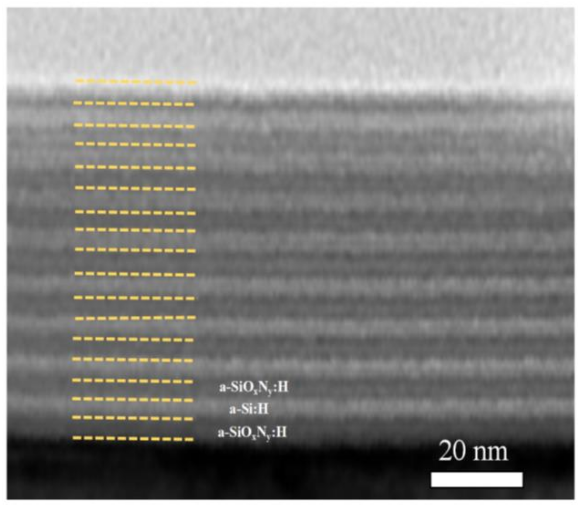
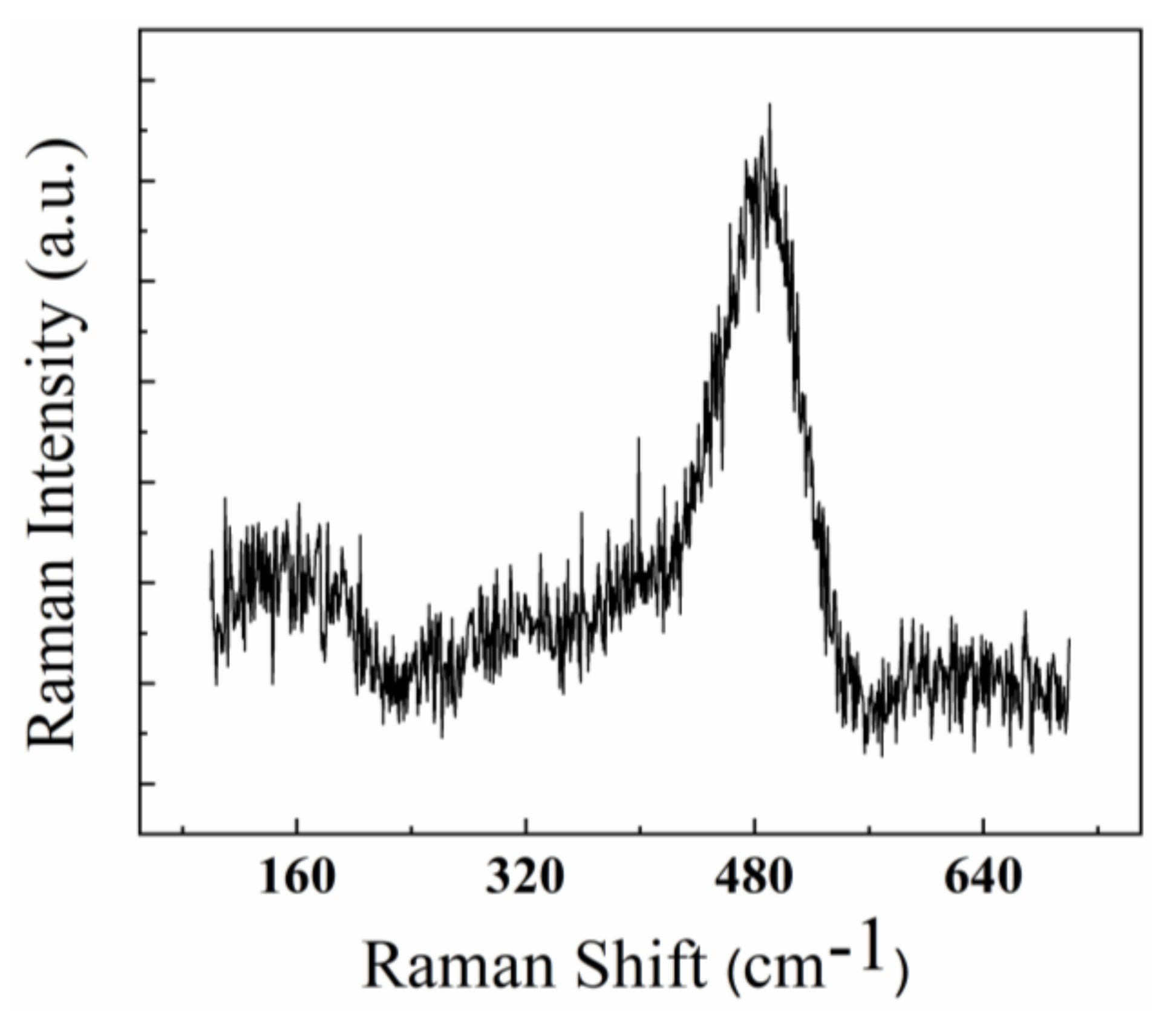
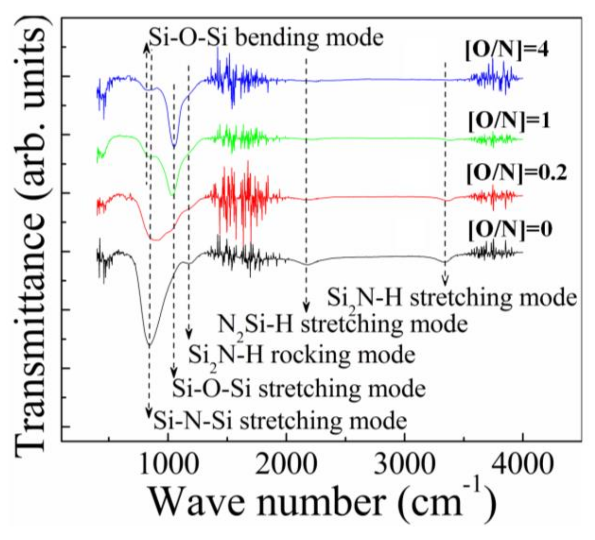
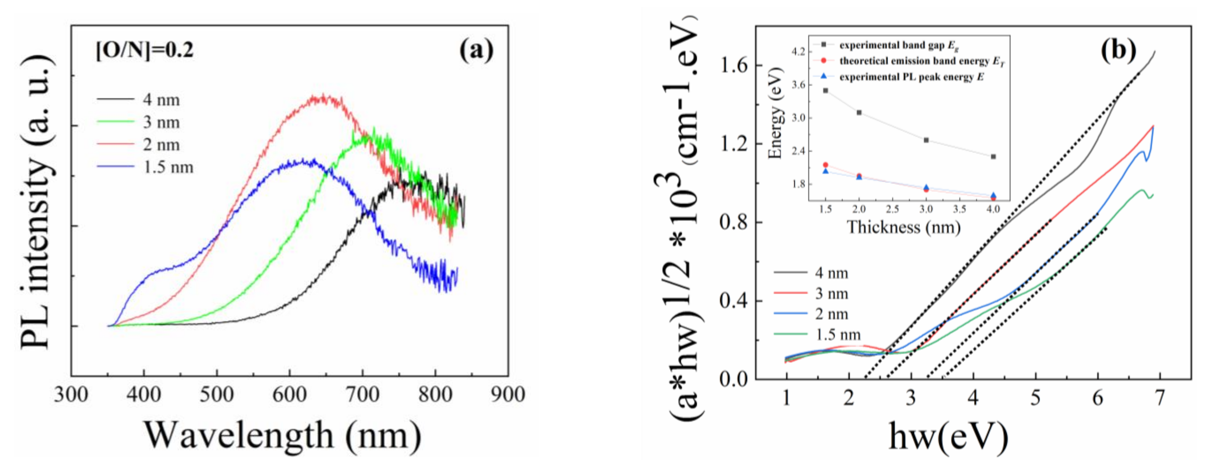
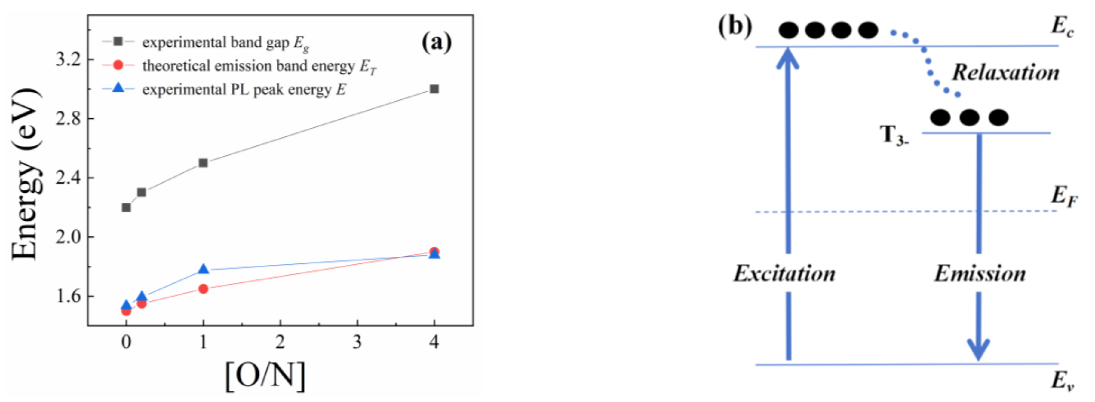
3. Results and Discussion

In order to visually observe the structure of the sample, the cross-section TEM micrographs of the multilayer structures were measured. In Figure 1, the micrograph of an eight-period a-Si/a-SiOxNy:H multilayer film with a 4 nm a-Si:H layer and a 4 nm a-SiOxNy:H layer when the oxygen/nitride ratio ([O/N]) is 0.2 in the a-SiOxNy:H sublayer (sample B) is given as a representative. It can be seen that the a-Si:H sublayer (well layer) with a thickness of 4 nm and the a-SiOxNy:H sublayer (barrier layer) with a thickness of 4 nm can be clearly characterized. Meanwhile, as shown in Figure 2, the transverse–acoustic vibration mode (160 cm−1) and transverse–optical vibration mode (480 cm−1) of Raman spectra for amorphous silicon are obtained, which indicate that the structures of these samples are a-Si/a-SiOxNy:H multilayer structures.
For multilayer samples with a 4 nm a-Si:H layer and a 4 nm a-SiOxNy:H layer, the room-temperature PL spectra with different values of [O/N] are shown in Figure 3I. The strong and stable red–orange PL from the multilayer films could be seen by the naked eye when the samples were illuminated with 325 nm radiation. Photographs of the PL from the multilayer films with different values of [O/N] are presented in the inset of Figure 3I. As shown in Figure 3I, the peak position and intensity of the PL strongly depend on the value of [O/N]. When the [O/N] ratio is zero, the multilayer sample with the a-SiNy:H barrier shows a broad PL spectrum peaking at 800 nm with a full width at half maximum (FWHM) near 240 nm, corresponding to the half-width of 0.51 eV in photon energy. The peak position of the PL spectra from the samples with an a-SiOxNy:H barrier varies from 800 nm to 660 nm with an increase in the oxygen/nitride ratio ([O/N]) in the a-SiOxNy:H sublayer. Figure 3II shows the integrated PL intensity and the PL peak positions as a function of the oxygen/nitride ratio ([O/N]) in the barrier layer. The intensity of PL from the samples increases first and then decreases with an increase in the [O/N] ratio.
It should be noted that the barrier materials used in the multilayer structures are the a-SiOxNy:H films. The PL from a-SiOxNy:H films has been reported by several authors, so it is necessary to analyze whether the luminescence of a-Si/a-SiOxNy: H multilayer films originates from the a-Si sublayer or the a-SiOxNy: H sublayer. For this purpose, PL measurements for the a-SiOxNy:H films were also taken. Figure 3III shows the PL spectra of the a-SiOxNy:H films with different values of [O/N], which were used as the barrier layer in multilayer samples. As shown in Figure 3III, all the a-SiOxNy:H films show the PL peaking at 390 nm. We notice that no distinct PL peaks were observed in the range of 750 nm to 650 nm for a-SiOxNy:H films, whereas the peak position of PL from the a-Si/a-SiOxNy:H multilayer samples varied in this range. Therefore, we conclude that the PL spectra from multilayer films shown in Figure 3I are not attributed to luminescent emission from the a-SiOxNy:H sublayer. The results shown in Figure 3I indicate that the interface between the barrier layer (a-SiOxNy:H) and the well layer (a-Si) plays an important role in the light emission of the a-Si/a-SiOxNy:H multilayer samples. When the oxygen/nitride ratio ([O/N]) in the barrier increases gradually, the PL peak position shifts from 800 nm to 660 nm.
In order to examine the local bonding configurations in a-Si/a-SiOxNy:H multilayer films, the FTIR spectra were measured. For a-Si/a-SiOxNy:H multilayer films with a 4 nm a-Si:H layer and a 4 nm a-SiOxNy:H layer, the FTIR spectra with different values of [O/N] are shown in Figure 4. It can be seen that, when the [O/N] ratio is zero, the Si–N-Si stretching mode, Si2N–H rocking mode, N2Si-H stretching mode, and Si2N–H stretching mode observed at ~837 cm−1, ~1176 cm−1, ~2169 cm−1, and ~3343 cm−1, respectively, can be obtained. With an increase in the [O/N] ratio, the Si-O-Si bending mode and Si-O-Si stretching mode observed at ~816 cm−1 and ~1052 cm−1 become stronger, and the N-related vibration peaks become weaker. These results indicate that, as the [O/N] ratio increases, the influence of Si-O-Si bonding on the interfacial properties of multilayer films becomes significant. As discussed in the PL spectra shown in Figure 3I, the PL peak position shifts from 800 nm to 660 nm as the [O/N] ratio increases, which indicates that the PL is affected by the Si-O-Si bonds.
The room-temperature photoluminescence results are shown in Figure 5a for a-Si/a-SiOxNy:H multilayer films with different a-Si layer thicknesses when the [O/N] ratio is 0.2 in the a-SiOxNy:H sublayer. It can be seen that, when the a-Si layer thickness is 4 nm, the peak of PL is at about 780 nm. As the a-Si layer thickness decreases, the blue shift of PL can be obtained. When the a-Si layer thickness is 1.5 nm, the peak of PL shifts to 620 nm. From these results, it can be demonstrated that the light emission is dominated by the a-Si:H sublayer. Moreover, the reasons for the blue shift of PL are further investigated by the optical transmittance in the UV–visible range. In Figure 5b, the experimental band gap (Eg) evaluated using a Tauc plot [17] and the peak energy of PL (E) are shown. It can be observed that the experimental band gap (Eg) increases with the decrease in the thickness of the a-Si:H sublayer. According to the reports [18], the blue shift of Eg should be caused by the quantum confinement effect in the a-Si:H sublayer. From Figure 5b, it can also be noted that, for all samples, the value of PL energy E is smaller than that of the band gap, which implies that the origin of light emission should be caused by the recombination of electrons and holes in the band tail of the a-Si:H sublayer. According to the reports [19], the origin of PL in the a-Si/a-SixNy:H multilayer has been discussed, and it is related to electronic transitions between the T3-level and the valence band. The value of emission band energy ET can be expressed approximately as ET = Eg/2 + 0.4, where Eg is the experimental band gap of multilayer films. In Figure 5b, the energy of ET is given. It can be seen that the energy of ET is compatible with the PL peak energy E, indicating that the origin of PL in a-Si:H/a-SiOxNy:H multilayer films is related to the T3−level of the silicon dangling bond. In Figure 6b, a level diagram for the silicon dangling bond of the a-Si:H film is given. Ec and Ev represent the edge of the conduction and valance bands, respectively. EF is the Fermi level in approximately the middle of the band gap. T3− is the negatively charged silicon dangling bond. The effective correlation energy between EF and T3− is approximately 0.4 eV.
In order to further investigate the mechanism of light emission for the a-Si:H/a-SiOxNy:H multilayer films with a 4 nm a-Si:H layer and a 4 nm a-SiOxNy:H layer, the [O/N] ratio dependence of the experimental PL peak energy E, experimental band gap Eg, and theoretical emission band energy ET are given in Figure 6a. It is shown that there is a similar change tendency for Eg and E as the [O/N] ratio increases, which implies that the blue shift of the band gap may be related to the Si-O-Si bonds, as discussed with FTIR. It has been reported that, for a–SiNx:H and a–SiCx:H films [20], the band gap energy will increase as the nitrogen or carbon content increases, and this will lead to a blue shift of Eg. As a result, for a-Si:H/a-SiOxNy:H multilayer films with different kinds of barrier materials, when increasing the oxygen/nitride ratio ([O/N]), the nitrogen and/or oxygen alloying induces structural disorder at the interface, resulting in an increase in the width of the localized states, which leads to an increase in the band gap energy. Meanwhile, it can be seen that the energy of ET is compatible with the PL peak energy E when there is an increase in the oxygen/nitride ratio ([O/N]), which indicates that the origin of the PL of multilayer samples is still related to the T3− level of the silicon dangling bond. Consequently, it can be suggested that, in a-Si:H/a-SiOxNy:H multilayer films, the electrons in the a-Si:H sublayer can be excited by high-energy photons (325 nm) to a highly excited-state energy level and then relax to the T3−level by emitting phonons, before radiatively recombining with holes at the valence band accompanied by light emission, as shown in Figure 6b.
As discussed above, for multilayer films of a-Si/a-SiOxNy:H, the properties of PL will be influenced by the thickness of the sublayer and the oxygen/nitride ratio ([O/N]) in the barrier material, and the nitrogen and/or oxygen alloying induces structural disorder at the interface, resulting in an increase in the width of the localized states. In order to further investigate the luminescent properties of a-Si/a-SiOxNy:H multilayer films, the PL spectra of the multilayer samples with different thicknesses of the a-Si sublayer as a function of the oxygen/nitride ratio ([O/N]) are measured. Figure 7a–d give the PL spectra of the multilayer samples with different thicknesses of the a-Si sublayer under different [O/N] ratios. The PL peak positions and integrated PL intensity, as functions of the [O/N] ratio in the barrier layer for samples with different a-Si sublayer thicknesses, are also shown in Figure 7e,f. It can be found that, for all samples with different [O/N] ratios, the blue shift of PL peak energy arises from the decrease in a-Si:H thickness. As shown in Figure 7e, it can be seen that, upon increasing the oxygen/nitride ratio ([O/N]), the PL peak position shifts towards lower wavelengths. And the blue shift of the PL peak occurs at a faster rate when the [O/N] ratio is small. As the [O/N] ratio gradually increases, the shift of the peak position gradually becomes smoother. Meanwhile, for samples with a larger [O/N] ratio, the influence of a-Si sublayer thickness on the shift of the luminescence peak position becomes significant. The results indicate that the addition of oxygen atoms introduces a large number of localized states at the interface, causing a blue shift in the emission’s peak position. With the increase in oxygen atoms, the localized states gradually tend to saturate, and the quantum phenomenon caused by the change in sublayer thickness becomes more pronounced. Figure 7e gives the integrated PL intensity as a function of the [O/N] ratio for samples with different a-Si sublayer thicknesses. It can be seen that, when the thickness of the a-Si sublayer is 4 nm, the intensity of PL can be enhanced by increasing the [O/N] ratio, and, when the [O/N] ratio becomes larger, the intensity of PL begins to weaken, which indicates that localized states caused by oxygen atoms not only introduce more luminescent centers but also increase the disorder at the interface, leading to a decrease in luminescent intensity. At the same time, it can be seen that, when the thickness of the a-Si sublayer decreases to 3 nm and 2 nm, as the [O/N] ratio increases, the intensity of PL first decreases, then increases, and then decreases. When the thickness of the a-Si sublayer is further reduced (to 1.5 nm), the intensity of PL decreases continuously as the [O/N] ratio increases. As a result, this indicates that, as the thickness of the a-Si sublayer decreases, the increase in the [O/N] ratio is more likely to cause an increase in disordered states, leading to a decrease in luminescence intensity. For a-Si/a-SiOxNy:H multilayer films with a thinner a-Si sublayer, an appropriate value of [O/N] is required to achieve luminescence enhancement; here, the appropriate value of [O/N] is one.
In a-Si-based materials, one usually considers the delocalized state (extended state) and the band tail state (weakly localized state) in the light absorption and emission processes [21]. It is well known that a blue shift of the optical absorption edge energy is due to the quantum confinement of carriers in a-Si multilayer structures. Since the band edge shifts to higher energy with a decrease in the a-Si sublayer thickness, the blue shift of the band tail state also occurs. When electrons and holes are excited to higher-energy states, and then due to the thermalization process, photo-generated carriers relax to the states of the band tails. Radiative recombination then occurs in those states. Thus, we speculate that the recombination of electrons and holes in the band tail of an a-Si:H sublayer embedded in an a-Si/a-SiOxNy:H multilayer structure may be responsible for the emission of PL from multilayer structures. We also notice that the barrier material plays an important role in the light emission of the multilayer structure. By adjusting the oxygen/nitride ratio ([O/N]) in the barrier layer, the PL peak position can be tuned from 800 nm to 660 nm. This could be because the nitrogen and/or oxygen alloying induces structural disorder at the interface, leading to an increase in the band gap energy. The localized states caused by oxygen atoms not only increase the disorder at the interface but also introduce more luminescent centers, leading to an increase in luminescent intensity. The increase in the [O/N] ratio will introduce the localized states related to silicon dangling bonds, which are responsible for the luminescence in a-Si/a-SiOxNy:H multilayer samples, as discussed in Figure 6b.

4. Conclusions

The PL characteristics of a-Si/a-silicon oxynitride multilayer films fabricated using a VHF-PECVD system have been studied. The interface between the a-SiOxNy:H barrier layer and the a-Si well layer and the thickness of the a-Si well layer play important roles in light emission. By changing the oxygen/nitride ratio (O/N) of the barrier layer, the PL peak position can be tuned from 800 nm (1.55 eV) to 660 nm (1.88 eV). With a decrease in the a-Si well layer thickness, a blue shift in the luminescence energy and optical absorption edge energy is observed. The interface and size dependence of the PL spectrum can be explained by the radiative recombination of carriers localized in the band tail state of the a-Si layer. It is found that the localized states caused by increasing the [O/N] ratio not only increase disorder at the interface but also introduce more luminescent centers, leading to an increase in luminescent intensity. For a-Si/a-SiOxNy:H samples with thinner a-Si sublayers, an appropriate value of [O/N] is required to achieve luminescence enhancement; here, the appropriate value of [O/N] is one.

Author Contributions

C.S. and X.W. conceived and designed the experiments; X.W. and J.S. performed the experiments; X.W. supervised this article. All authors have read and agreed to the published version of the manuscript.

Funding

This work was supported by the Self-innovation Research Funding Project of Hanjiang Laboratory (HJL202202A008) and University-enterprise Collaborative Innovation Center for Big Health Industry (2022 Hybribio Special Project–0002/b22088).

Institutional Review Board Statement

Not applicable.

Informed Consent Statement

Not applicable.

Data Availability Statement

Data are contained within the article.

Conflicts of Interest

The authors declare no conflicts of interest.

References

  1. Pavesi, L.; Dal Negro, L.; Cazzanelli, M.; Pucker, G.; Gaburro, Z.; Prakash, G.C.; Franzo, G.; Priolo, F. Optical gain in silicon nanocrystals. Natures 2001, 4293, 162–173. [Google Scholar] [CrossRef]
  2. Meng, L.; Li, S.; Chen, H.; Lei, M.; Yu, G.; Wen, P.; Fu, J.; Jiang, S.; Zong, H.; Li, D.; et al. In-situ fabricated amorphous silicon quantum dots embedded in silicon nitride matrix: Photoluminescence control and electroluminescence device fabrication. J. Lumin. 2023, 261, 119913. [Google Scholar] [CrossRef]
  3. Hegedüs, N.; Balázsi, K.; Balázsi, C. Silicon Nitride and Hydrogenated Silicon Nitride Thin Films: A Review of Fabrication Methods and Applications. Materials 2021, 14, 5658. [Google Scholar] [CrossRef] [PubMed]
  4. Tuan, N.T.; Thu, V.V.; Trung, D.Q.; Tu, N.; Tran, M.T.; Duong, P.H.; Anh, T.X.; Hong, N.T.; Loan, P.K.; Tam, T.T.H.; et al. Huy, On the origin of photoluminescence enhancement of Si nanocrystals on silica glass template and Si/SiO2 superlattice. Phys. B Condens. Matter 2023, 662, 414970. [Google Scholar] [CrossRef]
  5. Dey, P.P.; Khare, A. Fabrication of luminescent a-Si: SiO2 structures by direct irradiation of high power laser on silicon surface. Appl. Surf. Sci. 2014, 307, 77–85. [Google Scholar] [CrossRef]
  6. Bonilla, R.S.; Al-Dhahir, I.; Yu, M.; Hamer, P.; Altermatt, P.P. Altermatt, Charge fluctuations at the Si-SiO2 interface and its effect on surface recombination in solar cells. Sol. Energy Materials Sol. Cells 2020, 215, 110649. [Google Scholar] [CrossRef]
  7. Sondhi, K.; Sharangpani, R.; Tirukkonda, R.; Nag, J.; Guo, X.-C.; Gribelyuk, M.A.; Makala, R.S.; Kanakamedala, S. Extending area selective deposition of ruthenium onto 3D SiO2-Si multilayer stacks. J. Vac. Sci. Technol. A 2023, 41, 050402. [Google Scholar] [CrossRef]
  8. González-Flores, K.E.; Frieiro, J.L.; Horley, P.; Pérez-García, S.A.; Palacios-Huerta, L.; Moreno, M.; López-Vidrier, J.; Hernández, S.; Garrido, B.; Morales-Sánchez, A. Ultraviolet, visible and near infrared photoresponse of SiO2/Si/SiO2 multilayer system into a MOS capacitor. Mater. Sci. Semicond. Process. 2021, 134, 106009. [Google Scholar] [CrossRef]
  9. Torchynska, T.; Khomenkova, L.; Slaoui, A. Modification of light emission in si-rich silicon nitride films versus stoichiometry and excitation light energy. J. Electron. Mat. 2018, 47, 3927–3933. [Google Scholar] [CrossRef]
  10. Liu, Q.; Chen, X.; Li, H.; Guo, Y.; Song, J.; Zhang, W.; Song, C.; Huang, R.; Lin, Z. Effect of Thermal Annealing on the Photoluminescence of Dense Si Nanodots Embedded in Amorphous Silicon Nitride Films. Micromachines 2021, 12, 354. [Google Scholar] [CrossRef] [PubMed]
  11. Tiour, F.; Benyahia, B.; Brihi, N.; Sari, A.; Mahmoudi, B.; Manseri, A.; Guenda, A. Opto-structural properties of Si-rich SiNx with different stoichiometry. Appl. Phys. A 2020, 126, 59. [Google Scholar] [CrossRef]
  12. Xu, W.; Tang, H.; Zhang, Q.; Zhou, N.; Shen, Y. Room-temperature deposition of low H-content SiNx/SiNxOy thin films using a specially designed PECVD system. Surf. Coatings Technol. 2020, 402, 126506. [Google Scholar] [CrossRef]
  13. Hang, L.; Liu, W.; Xu, J.; Yang, C.; Zhou, S. Effects of various substrate materials on microstructural and optical properties of amorphous silicon oxynitride thin films deposited by plasma-enhanced chemical vapor deposition. Thin Solid Films 2020, 709, 138186. [Google Scholar] [CrossRef]
  14. Hegedüs, N.; Balázsi, C.; Kolonits, T.; Olasz, D.; Sáfrán, G.; Serényi, M.; Balázsi, K. Investigation of the RF Sputtering Process and the Properties of Deposited Silicon Oxynitride Layers under Varying Reactive Gas Conditions. Materials 2022, 15, 6313. [Google Scholar] [CrossRef] [PubMed]
  15. Zhang, P.; Zhang, L.; Wu, Y.; Wang, S.; Ge, X. High photoluminescence quantum yields generated from N-Si-O bonding states in amorphous silicon oxynitride films: Erratum. Optics Express 2022, 30, 40626. [Google Scholar] [CrossRef] [PubMed]
  16. Ma, H.P.; Lu, H.L.; Yang, J.H.; Li, X.X.; Wang, T.; Huang, W.; Yuan, G.J.; Komarov, F.; Zhang, D. Measurements of microstructural, chemical, optical, and electrical properties of silicon-oxygen-nitrogen films prepared by plasma-enhanced atomic layer deposition. Nanomaterials 2018, 8, 1008. [Google Scholar] [CrossRef] [PubMed]
  17. Nakajima, A.; Sugita, Y.; Kawamura, K.; Tomita, H.; Yok, N. Oyama, Microstructure and optical absorption properties of Si nanocrystals fabricated with low-pressure chemical-vapor deposition. J. Appl. Phys. 1996, 80, 4006–4011. [Google Scholar] [CrossRef]
  18. Singh, J. Effective mass of charge carriers in amorphous semiconductors and its applications. J. Non-Cryst. Solids 2002, 299–302, 444–448. [Google Scholar]
  19. Song, C.; Huang, R.; Wang, X.; Guo, Y.Q.; Song, J. Tunable red light emission from a-Si: H/a-SiNx multilayers. Opt. Materials Express 2013, 3, 664–670. [Google Scholar] [CrossRef]
  20. Kato, H.; Kashio, N.; Ohki, Y.; Seol, K.S.; Noma, T. Band-tail photoluminescence in hydrogenated amorphous silicon oxynitride and silicon nitride films. J. Appl. Phys. 2003, 93, 239–244. [Google Scholar] [CrossRef]
  21. Wang, M.; Xie, M.; Ferraioli, L.; Yuan, Z.; Li, D.; Yang, D.; Pavesi, L. Light emission properties and mechanism of low-temperature prepared amorphous SiNx films. I. Room-temperature band tail states photoluminescence. J. Appl. Phys. 2008, 104, 083504. [Google Scholar] [CrossRef]
Figure 1. Cross-section TEM image of a-Si/a-SiOxNy:H multilayer film with 4 nm a-Si:H layer and 4 nm a-SiOxNy:H layer when [O/N] ratio is 0.2 (the interface between a-Si layer and a-SiOxNy:H layer is indicated by dotted line).
Coatings 14 00977 g001
Figure 2. Raman spectra of the a-Si/a-SiOxNy:H multilayer film with 4 nm a-Si:H layer and 4 nm a-SiOxNy:H layer when [O/N] ratio is 0.2.
Coatings 14 00977 g002
Figure 3. (I) PL spectra of the a-Si/a-SiOxNy:H multilayer samples with different values of [O/N]. (II) The integrated PL intensity and the PL peak positions as a function of [O/N] ratio in the barrier layer (arrows are used to indicate the coordinates corresponding to the data). (III) PL spectra of the a-SiOxNy:H films with different values of [O/N], which were used as the barrier layer in the multilayer structure.
Coatings 14 00977 g003
Figure 4. FTIR spectra of the a-Si/a-SiOxNy:H multilayer samples with different values of [O/N].
Coatings 14 00977 g004
Figure 5. (a) PL spectra of the a-Si/a-SiOxNy:H multilayer films with different a-Si sublayer thickness. (b) Tauc plots of the a-Si/a-SiOxNy:H multilayer films with different a-Si sublayer thickness. The inset presents the a-Si:H sublayer thickness dependence of the experimental band gap Eg, theoretical emission band energy ET, and experimental PL peak energy E.
Coatings 14 00977 g005
Figure 6. (a) The [O/N] ratio dependence of the experimental band gap Eg, theoretical emission band energy ET, and experimental PL peak energy E. (b) Schematic energy band diagram of the a-Si:H sublayer. The defect state T3−level of the silicon dangling bond and the exciton recombination processes are illustrated in the diagram.
Coatings 14 00977 g006
Figure 7. PL spectra of the a-Si/a-SiOxNy:H multilayer samples with different a-Si sublayer thickness. (a) [O/N] = 0. (b) [O/N] = 0.2. (c) [O/N] = 1. (d) [O/N] = 4. (e) The PL peak positions as a function of [O/N] ratio in the barrier layer for samples with different a-Si sublayer thickness. (f) The integrated PL intensity as a function of [O/N] ratio in the barrier layer for samples with different a-Si sublayer thickness.
Coatings 14 00977 g007
Table 1. Experimental parameters used to deposit a-Si/a-SiOxNy:H multilayer films.
SampleSiOxNy:H Sublayera-Si Sublayer
SiH4
(sccm)
NH3
(sccm)
O2
(sccm)
[O/N]Thickness
(nm)
SiH4
(sccm)
H2
(sccm)
Thickness
(nm)
A2.515-041.51604
B2.5151.50.241.51604
C2.5105141.51604
D2.5510441.51604
E2.515-041.51603
F2.515-041.51602
G2.515-041.51601.5
H2.5151.50.241.51603
I2.5151.50.241.51602
J2.5151.50.241.51601.5
K2.5105141.51603
L2.5105141.51602
M2.5105141.51601.5
N2.5510441.51603
O2.5510441.51602
P2.5510441.51601.5
Disclaimer/Publisher’s Note: The statements, opinions and data contained in all publications are solely those of the individual author(s) and contributor(s) and not of MDPI and/or the editor(s). MDPI and/or the editor(s) disclaim responsibility for any injury to people or property resulting from any ideas, methods, instructions or products referred to in the content.

