
Study of Grain Boundary: From Crystallization Engineering to Machine Learning


Abstract
1. Introduction
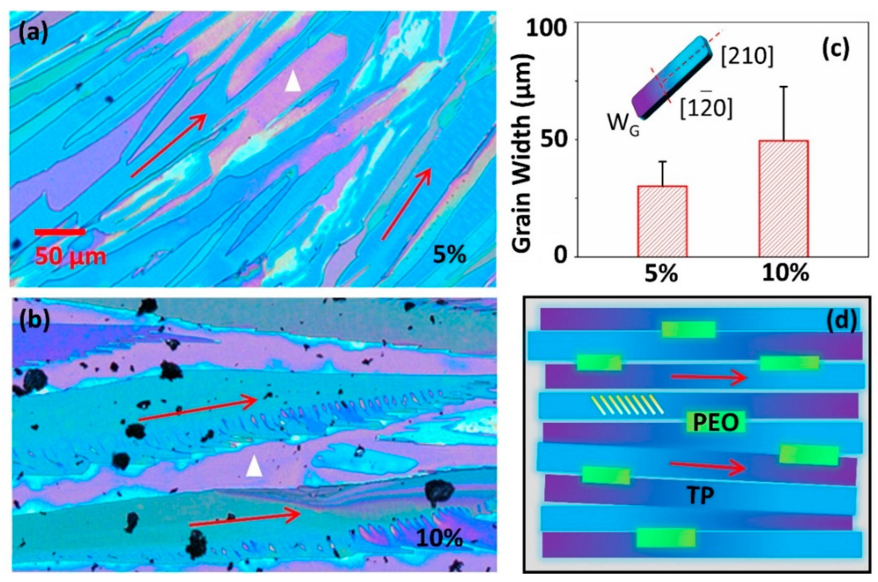
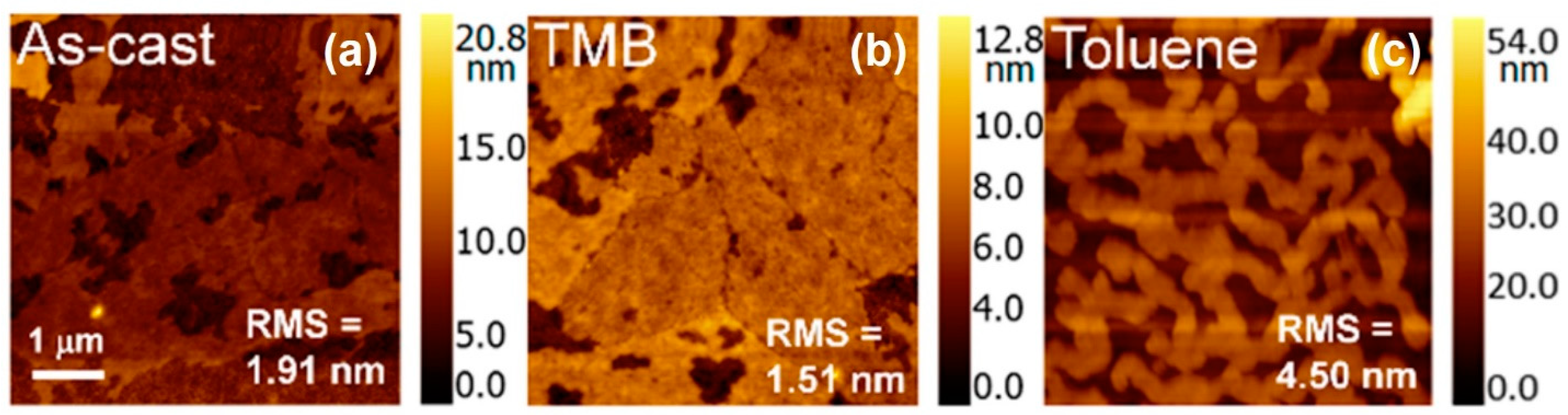
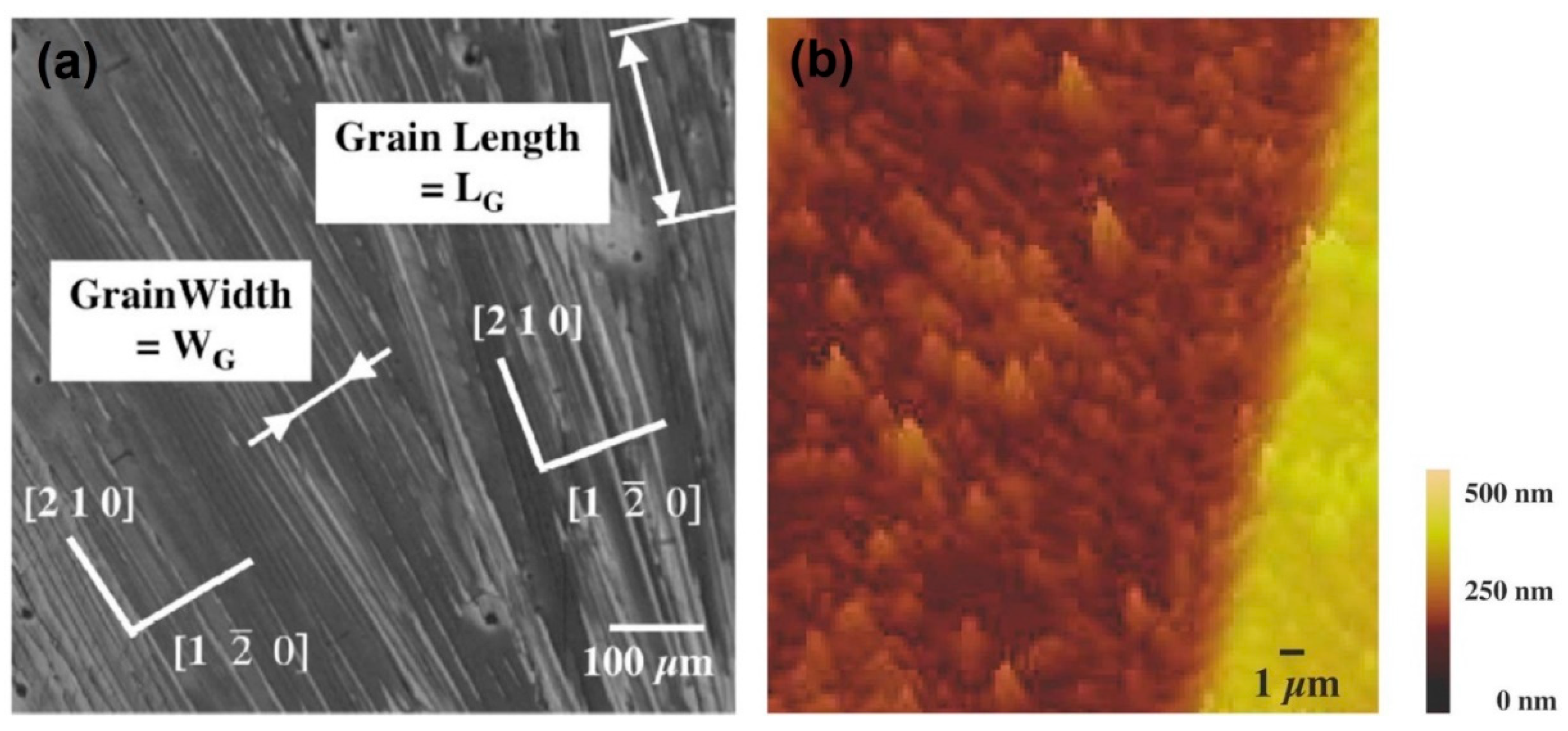
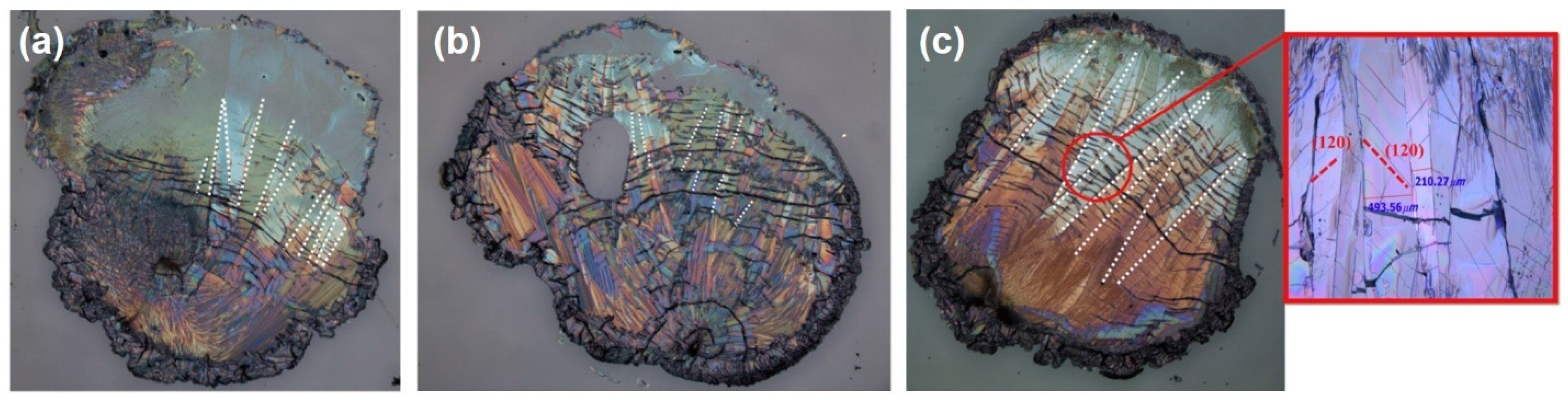
2. Crystallization Engineering in Grain Boundaries
3. Machine Learning in Grain Boundaries
4. Conclusions
Author Contributions
Funding
Institutional Review Board Statement
Informed Consent Statement
Data Availability Statement
Conflicts of Interest
References
- Shen, T.; Zhou, H.; Liu, X.; Fan, Y.; Mishra, D.D.; Fan, Q.; Yang, Z.; Wang, X.; Zhang, M.; Li, J. Wettability Control of Interfaces for High-Performance Organic Thin-Film Transistors by Soluble Insulating Polymer Films. ACS Omega 2020, 5, 10891–10899. [Google Scholar] [CrossRef] [PubMed]
- Hadipour, A. Utilizing Metal Oxide Thin Films for Device Engineering of Solution-Processed Organic Multi-Junction Solar Cells. Coatings 2024, 14, 525. [Google Scholar] [CrossRef]
- Foggiatto, A.L.; Takeichi, Y.; Ono, K.; Suga, H.; Takahashi, Y.; Fusella, M.A.; Dull, J.T.; Rand, B.P.; Kutsukake, K.; Sakurai, T. Study of local structure at crystalline rubrene grain boundaries via scanning transmission X-ray microscopy. Org. Electron. 2019, 74, 315–320. [Google Scholar] [CrossRef]
- Kondo, M.; Kajitani, T.; Uemura, T.; Noda, Y.; Ishiwari, F.; Shoji, Y.; Araki, T.; Yoshimoto, S.; Fukushima, T.; Sekitani, T. Highly-ordered Triptycene Modifier Layer Based on Blade Coating for Ultraflexible Organic Transistors. Sci. Rep. 2019, 9, 9200. [Google Scholar] [CrossRef]
- Manaka, T.; Matsubara, K.; Abe, K.; Iwamoto, M. Direct Observation of Anisotropic Carrier Transport in Organic Semiconductor by Time-Resolved Microscopic Optical Second-Harmonic Imaging. Appl. Phys. Express 2013, 6, 101601. [Google Scholar] [CrossRef]
- Benzarti, Z.; Khalfallah, A. Recent Advances in the Development of Thin Films. Coatings 2024, 14, 878. [Google Scholar] [CrossRef]
- He, Z.; Asare-Yeboah, K.; Bi, S. Advances in Charge Carrier Mobility of Diketopyrrolopyrrole-Based Organic Semiconductors. Coatings 2024, 14, 1080. [Google Scholar] [CrossRef]
- Kim, K.; Lee, Z.; Regan, W.; Kisielowski, C.; Crommie, M.F.; Zettl, A. Grain Boundary Mapping in Polycrystalline Graphene. ACS Nano 2011, 5, 2142–2146. [Google Scholar] [CrossRef]
- Park, J.-S.; Walsh, A. Modeling Grain Boundaries in Polycrystalline Halide Perovskite Solar Cells. Annu. Rev. Condens. Matter Phys. 2021, 12, 95–109. [Google Scholar] [CrossRef]
- Wang, L.; Chen, S.; Li, W.; Wang, K.; Lou, Z.; Shen, G. Grain-Boundary-Induced Drastic Sensing Performance Enhancement of Polycrystalline-Microwire Printed Gas Sensors. Adv. Mater. 2019, 31, 1804583. [Google Scholar] [CrossRef]
- Zhang, J.; Xu, L.; Han, Y.; Zhao, L.; Xiao, B. New perspectives on the grain boundary misorientation angle dependent intergranular corrosion of polycrystalline nickel-based 625 alloy. Corros. Sci. 2020, 172, 108718. [Google Scholar] [CrossRef]
- Zhao, D.; Chen, J.; Wang, B.; Wang, G.; Chen, Z.; Yu, J.; Guo, X.; Huang, W.; Marks, T.J.; Facchetti, A. Engineering Intrinsic Flexibility in Polycrystalline Molecular Semiconductor Films by Grain Boundary Plasticization. J. Am. Chem. Soc. 2020, 142, 5487–5492. [Google Scholar] [CrossRef] [PubMed]
- Luan, D.; Wang, Y.; Li, M.; Chen, J. The grain boundary effect on shock induced spallation of polycrystalline uranium. Int. J. Mech. Sci. 2022, 228, 107491. [Google Scholar] [CrossRef]
- Dmitriev, A.I.; Nikonov, A.Y.; Shugurov, A.R.; Panin, A.V. The Role of Grain Boundaries in Rotational Deformation in Polycrystalline Titanium under Scratch Testing. Phys. Mesomech. 2019, 22, 365–374. [Google Scholar] [CrossRef]
- Perrin, A.E.; Schuh, C.A. Stabilized Nanocrystalline Alloys: The Intersection of Grain Boundary Segregation with Processing Science. Annu. Rev. Mater. Res. 2021, 51, 241–268. [Google Scholar] [CrossRef]
- Ming, K.; Li, L.; Li, Z.; Bi, X.; Wang, J. Grain boundary decohesion by nanoclustering Ni and Cr separately in CrMnFeCoNi high-entropy alloys. Sci. Adv. 2019, 5, eaay0639. [Google Scholar] [CrossRef]
- Utt, D.; Stukowski, A.; Albe, K. Grain boundary structure and mobility in high-entropy alloys: A comparative molecular dynamics study on a Σ11 symmetrical tilt grain boundary in face-centered cubic CuNiCoFe. Acta Mater. 2020, 186, 11–19. [Google Scholar] [CrossRef]
- Zhao, H.; De Geuser, F.; Kwiatkowski da Silva, A.; Szczepaniak, A.; Gault, B.; Ponge, D.; Raabe, D. Segregation assisted grain boundary precipitation in a model Al-Zn-Mg-Cu alloy. Acta Mater. 2018, 156, 318–329. [Google Scholar] [CrossRef]
- Devaraj, A.; Wang, W.; Vemuri, R.; Kovarik, L.; Jiang, X.; Bowden, M.; Trelewicz, J.R.; Mathaudhu, S.; Rohatgi, A. Grain boundary segregation and intermetallic precipitation in coarsening resistant nanocrystalline aluminum alloys. Acta Mater. 2019, 165, 698–708. [Google Scholar] [CrossRef]
- Fan, T.; Ruan, Z.; Lin, L.; Liu, X.; Luo, H. First-Principles Study of Physical Properties of (110) Symmetric Small-Angle Tilting Grain Boundary with Full Dislocation in Aluminum. Coatings 2024, 14, 1533. [Google Scholar] [CrossRef]
- Xing, W.; Kalidindi, A.R.; Amram, D.; Schuh, C.A. Solute interaction effects on grain boundary segregation in ternary alloys. Acta Mater. 2018, 161, 285–294. [Google Scholar] [CrossRef]
- Jang, H.-S.; Lee, B.-J. Effects of Zn on 〈c + a〉 slip and grain boundary segregation of Mg alloys. Scr. Mater. 2019, 160, 39–43. [Google Scholar] [CrossRef]
- Fischer, D.; Zagorac, D.; Küster, K.; Schön, J.C. Synthesis of Two Structurally Different MgO Films Containing Dioxygen Species: Dioxygen Embedded at Grain Boundaries, and as Components of a Superfilled Rock Salt Structure. Coatings 2024, 14, 1563. [Google Scholar] [CrossRef]
- Xin, R.; Liu, Z.; Sun, Y.; Wang, H.; Guo, C.; Ren, W.; Liu, Q. Understanding common grain boundary twins in Mg alloys by a composite Schmid factor. Int. J. Plast. 2019, 123, 208–223. [Google Scholar] [CrossRef]
- Zhou, X.; Li, X.; Lu, K. Size Dependence of Grain Boundary Migration in Metals under Mechanical Loading. Phys. Rev. Lett. 2019, 122, 126101. [Google Scholar] [CrossRef] [PubMed]
- Zheng, H.; Li, X.-G.; Tran, R.; Chen, C.; Horton, M.; Winston, D.; Persson, K.A.; Ong, S.P. Grain boundary properties of elemental metals. Acta Mater. 2020, 186, 40–49. [Google Scholar] [CrossRef]
- Phung, N.; Al-Ashouri, A.; Meloni, S.; Mattoni, A.; Albrecht, S.; Unger, E.L.; Merdasa, A.; Abate, A. The Role of Grain Boundaries on Ionic Defect Migration in Metal Halide Perovskites. Adv. Energy Mater. 2020, 10, 1903735. [Google Scholar] [CrossRef]
- Hou, Q.; Zhou, S.; Wei, Y.; Caro, J.; Wang, H. Balancing the Grain Boundary Structure and the Framework Flexibility through Bimetallic Metal–Organic Framework (MOF) Membranes for Gas Separation. J. Am. Chem. Soc. 2020, 142, 9582–9586. [Google Scholar] [CrossRef]
- Yu, S.; Siegel, D.J. Grain Boundary Softening: A Potential Mechanism for Lithium Metal Penetration through Stiff Solid Electrolytes. ACS Appl. Mater. Interfaces 2018, 10, 38151–38158. [Google Scholar] [CrossRef]
- Liang, H.; Zhang, L.; Wu, H. Exploration of Twin-Modified Grain Boundary Engineering in Metallic Copper Predominated Electromagnetic Wave Absorber. Small 2022, 18, 2203620. [Google Scholar] [CrossRef]
- Kazemi, A.; Yang, S. Effects of magnesium dopants on grain boundary migration in aluminum-magnesium alloys. Comput. Mater. Sci. 2021, 188, 110130. [Google Scholar] [CrossRef]
- Yang, H.; Wu, L.; Jiang, B.; Liu, W.; Song, J.; Huang, G.; Zhang, D.; Pan, F. Clarifying the roles of grain boundary and grain orientation on the corrosion and discharge processes of α-Mg based Mg-Li alloys for primary Mg-air batteries. J. Mater. Sci. Technol. 2021, 62, 128–138. [Google Scholar] [CrossRef]
- Gong, Z.; Zhao, W.; Guan, K.; Rao, P.; Zeng, Q.; Liu, J.; Feng, Z. Influence of grain boundary and grain size on the mechanical properties of polycrystalline ceramics: Grain-scale simulations. J. Am. Ceram. Soc. 2020, 103, 5900–5913. [Google Scholar] [CrossRef]
- Kohl, M.; Boštíková, K.; Slang, S.; Schmidová, E.; Kalendová, A. Use of 2D Sulfide and Oxide Compounds as Functional Semiconducting Pigments in Protective Organic Coatings Containing Zinc Dust. Coatings 2024, 14, 1009. [Google Scholar] [CrossRef]
- Karoutsos, V.; Florini, N.; Diamantopoulos, N.C.; Balourda, C.; Dimitrakopulos, G.P.; Bouropoulos, N.; Poulopoulos, P. On the Effect of Randomly Oriented Grain Growth on the Structure of Aluminum Thin Films Deposited via Magnetron Sputtering. Coatings 2024, 14, 1441. [Google Scholar] [CrossRef]
- Coleman, S.P.; Tschopp, M.A.; Weinberger, C.R.; Spearot, D.E. Bridging atomistic simulations and experiments via virtual diffraction: Understanding homophase grain boundary and heterophase interface structures. J. Mater. Sci. 2016, 51, 1251–1260. [Google Scholar] [CrossRef]
- Shi, R.; Shen, C.; Dregia, S.A.; Wang, Y. Form of critical nuclei at homo-phase boundaries. Scr. Mater. 2018, 146, 276–280. [Google Scholar] [CrossRef]
- Vitek, J.M. Influence of segregation on the diffraction effects from homophase interfaces. Ultramicroscopy 1987, 22, 197–206. [Google Scholar] [CrossRef]
- Gutierrez-Urrutia, I.; Archie, F.; Raabe, D.; Yan, F.-K.; Tao, N.-R.; Lu, K. Plastic accommodation at homophase interfaces between nanotwinned and recrystallized grains in an austenitic duplex-microstructured steel. Sci. Technol. Adv. Mater. 2016, 17, 29–36. [Google Scholar] [CrossRef]
- Kroonblawd, M.P.; Mathew, N.; Jiang, S.; Sewell, T.D. A generalized crystal-cutting method for modeling arbitrarily oriented crystals in 3D periodic simulation cells with applications to crystal–crystal interfaces. Comput. Phys. Commun. 2016, 207, 232–242. [Google Scholar] [CrossRef]
- Shi, R.; Heo, T.W.; Wood, B.C.; Wang, Y. Critical nuclei at hetero-phase interfaces. Acta Mater. 2020, 200, 510–525. [Google Scholar] [CrossRef]
- Fabbri, E.; Pergolesi, D.; Traversa, E. Ionic conductivity in oxide heterostructures: The role of interfaces. Sci. Technol. Adv. Mater. 2010, 11, 054503. [Google Scholar] [CrossRef] [PubMed]
- Zhou, S.; Han, J.; Sun, J.; Srolovitz, D.J. MoS2 edges and heterophase interfaces: Energy, structure and phase engineering. 2D Mater. 2017, 4, 025080. [Google Scholar] [CrossRef]
- Bausch, A.R.; Bowick, M.J.; Cacciuto, A.; Dinsmore, A.D.; Hsu, M.F.; Nelson, D.R.; Nikolaides, M.G.; Travesset, A.; Weitz, D.A. Grain Boundary Scars and Spherical Crystallography. Science 2003, 299, 1716–1718. [Google Scholar] [CrossRef] [PubMed]
- Banadaki, A.D.; Tschopp, M.A.; Patala, S. An efficient Monte Carlo algorithm for determining the minimum energy structures of metallic grain boundaries. Comput. Mater. Sci. 2018, 155, 466–475. [Google Scholar] [CrossRef]
- Homer, E.R.; Patala, S.; Priedeman, J.L. Grain Boundary Plane Orientation Fundamental Zones and Structure-Property Relationships. Sci. Rep. 2015, 5, 15476. [Google Scholar] [CrossRef] [PubMed]
- Randle, V. A methodology for grain boundary plane assessment by single-section trace analysis. Scr. Mater. 2001, 44, 2789–2794. [Google Scholar] [CrossRef]
- Kim, C.-S.; Rollett, A.D.; Rohrer, G.S. Grain boundary planes: New dimensions in the grain boundary character distribution. Scr. Mater. 2006, 54, 1005–1009. [Google Scholar] [CrossRef]
- Gruber, J.; George, D.C.; Kuprat, A.P.; Rohrer, G.S.; Rollett, A.D. Effect of anisotropic grain boundary properties on grain boundary plane distributions during grain growth. Scr. Mater. 2005, 53, 351–355. [Google Scholar] [CrossRef]
- Beladi, H.; Tari, V.; Rohrer, G.S. On Σ9 grain boundary plane orientation. Materialia 2022, 25, 101540. [Google Scholar] [CrossRef]
- Xie, Y.; Shibata, K.; Mizoguchi, T. A brute-force code searching for cell of non-identical displacement for CSL grain boundaries and interfaces. Comput. Phys. Commun. 2022, 273, 108260. [Google Scholar] [CrossRef]
- Cleri, F.; Keblinski, P.; Colombo, L.; Phillpot, S.R.; Wolf, D. Correlation between atomic structure and localized gap states in silicon grain boundaries. Phys. Rev. B 1998, 57, 6247–6250. [Google Scholar] [CrossRef]
- Gautam, A.; Ophus, C.; Lançon, F.; Radmilovic, V.; Dahmen, U. Atomic structure characterization of an incommensurate grain boundary. Acta Mater. 2013, 61, 5078–5086. [Google Scholar] [CrossRef]
- Wang, Z.L.; Kontra, R.; Kroeger, D.M.; Goyal, A.; Williams, R.K. Interface and grain boundary structures in YBa2Cu3O7-xand YBa2Cu4O8 materials. Interface Sci. 1994, 1, 321–337. [Google Scholar] [CrossRef]
- Lejček, P.; Hofmann, S. Thermodynamics and structural aspects of grain boundary segregation. Crit. Rev. Solid State Mater. Sci. 1995, 20, 1–85. [Google Scholar] [CrossRef]
- Merkle, K.L.; Smith, D.J. Atomic Structure of Symmetric Tilt Grain Boundaries in NiO. Phys. Rev. Lett. 1987, 59, 2887–2890. [Google Scholar] [CrossRef]
- Merkle, K.L. Atomic structure of grain boundaries. J. Phys. Chem. Solids 1994, 55, 991–1005. [Google Scholar] [CrossRef]
- Sato, Y.; Yamamoto, T.; Ikuhara, Y. Atomic Structures and Electrical Properties of ZnO Grain Boundaries. J. Am. Ceram. Soc. 2007, 90, 337–357. [Google Scholar] [CrossRef]
- Brandon, D.G.; Ralph, B.; Ranganathan, S.; Wald, M.S. A field ion microscope study of atomic configuration at grain boundaries. Acta Metall. 1964, 12, 813–821. [Google Scholar] [CrossRef]
- Bai, X.-M.; Vernon, L.J.; Hoagland, R.G.; Voter, A.F.; Nastasi, M.; Uberuaga, B.P. Role of atomic structure on grain boundary-defect interactions in Cu. Phys. Rev. B 2012, 85, 214103. [Google Scholar] [CrossRef]
- Nie, J.; Hu, C.; Yan, Q.; Luo, J. Discovery of electrochemically induced grain boundary transitions. Nat. Commun. 2021, 12, 2374. [Google Scholar] [CrossRef] [PubMed]
- Hu, T.; Yang, S.; Zhou, N.; Zhang, Y.; Luo, J. Role of disordered bipolar complexions on the sulfur embrittlement of nickel general grain boundaries. Nat. Commun 2018, 9, 2764. [Google Scholar] [CrossRef]
- Pan, Z.; Rupert, T.J. Effect of grain boundary character on segregation-induced structural transitions. Phys. Rev. B 2016, 93, 134113. [Google Scholar] [CrossRef]
- Konovalov, V.V.; Zangari, G.; Metzger, R.M. Highly Ordered Nanotopographies on Electropolished Aluminum Single Crystals. Chem. Mater. 1999, 11, 1949–1951. [Google Scholar] [CrossRef]
- Rabkin, E.I.; Shvindlerman, L.S.; Straumal, B.B. Grain Boundaries: Phase Transitions and Critical Phenomena. Int. J. Mod. Phys. B 1991, 5, 2989–3028. [Google Scholar] [CrossRef]
- Straumal, B.; Baretzky, B. Grain Boundary Phase Transitions and their Influence on Properties of Polycrystals. Interface Sci. 2004, 12, 147–155. [Google Scholar] [CrossRef]
- Rohrer, G.S. The role of grain boundary energy in grain boundary complexion transitions. Curr. Opin. Solid State Mater. Sci. 2016, 20, 231–239. [Google Scholar] [CrossRef]
- Straumal, B.B.; Ziȩba, P.; Gust, W. Grain boundary phase transitions and phase diagrams. Int. J. Inorg. Mater. 2001, 3, 1113–1115. [Google Scholar] [CrossRef]
- Haile, S.M.; Staneff, G.; Ryu, K.H. Non-stoichiometry, grain boundary transport and chemical stability of proton conducting perovskites. J. Mater. Sci. 2001, 36, 1149–1160. [Google Scholar] [CrossRef]
- Schaefer, M.; Fournelle, R.A.; Liang, J. Theory for intermetallic phase growth between cu and liquid Sn-Pb solder based on grain boundary diffusion control. J. Electron. Mater. 1998, 27, 1167–1176. [Google Scholar] [CrossRef]
- Han, J.; Vitek, V.; Srolovitz, D.J. Grain-boundary metastability and its statistical properties. Acta Mater. 2016, 104, 259–273. [Google Scholar] [CrossRef]
- Montes de Oca Zapiain, D.; Guziewski, M.; Coleman, S.P.; Dingreville, R. Characterizing the Tensile Strength of Metastable Grain Boundaries in Silicon Carbide Using Machine Learning. J. Phys. Chem. C 2020, 124, 24809–24821. [Google Scholar] [CrossRef]
- Combe, N.; Mompiou, F.; Legros, M. Disconnections kinks and competing modes in shear-coupled grain boundary migration. Phys. Rev. B 2016, 93, 024109. [Google Scholar] [CrossRef]
- Millett, P.C.; Selvam, R.P.; Bansal, S.; Saxena, A. Atomistic simulation of grain boundary energetics—Effects of dopants. Acta Mater. 2005, 53, 3671–3678. [Google Scholar] [CrossRef]
- Meiners, T.; Frolov, T.; Rudd, R.E.; Dehm, G.; Liebscher, C.H. Observations of grain-boundary phase transformations in an elemental metal. Nature 2020, 579, 375–378. [Google Scholar] [CrossRef]
- Zhang, J.; Rabe, J.P.; Koch, N. Grain-Boundary Evolution in a Pentacene Monolayer. Adv. Mater. 2008, 20, 3254–3257. [Google Scholar] [CrossRef]
- Weis, M.; Gmucová, K.; Nádaždy, V.; Majková, E.; Haško, D.; Taguchi, D.; Manaka, T.; Iwamoto, M. Grain Boundary Effect on Charge Transport in Pentacene Thin Films. Jpn. J. Appl. Phys. 2011, 50, 04DK03. [Google Scholar] [CrossRef]
- Seo, Y.; Lee, J.H.; Anthony, J.E.; Nguyen, K.V.; Kim, Y.H.; Jang, H.W.; Ko, S.; Cho, Y.; Lee, W.H. Effects of Grain Boundary Density on the Gas Sensing Properties of Triethylsilylethynyl-Anthradithiophene Field-Effect Transistors. Adv. Mater. Interfaces 2018, 5, 1701399. [Google Scholar] [CrossRef]
- Nguyen, K.V.; Payne, M.M.; Anthony, J.E.; Lee, J.H.; Song, E.; Kang, B.; Cho, K.; Lee, W.H. Grain Boundary Induced Bias Instability in Soluble Acene-Based Thin-Film Transistors. Sci. Rep. 2016, 6, 33224. [Google Scholar] [CrossRef]
- Rivnay, J.; Jimison, L.H.; Northrup, J.E.; Toney, M.F.; Noriega, R.; Lu, S.F.; Marks, T.J.; Facchetti, A.; Salleo, A. Large modulation of carrier transport by grain-boundary molecular packing and microstructure in organic thin films. Nat. Mater. 2009, 8, 952–958. [Google Scholar] [CrossRef] [PubMed]
- Minari, T.; Nemoto, T.; Isoda, S. Fabrication and characterization of single-grain organic field-effect transistor of pentacene. J. Appl. Phys. 2004, 96, 769–772. [Google Scholar] [CrossRef]
- Horowitz, G.; Hajlaoui, M.E. Mobility in Polycrystalline Oligothiophene Field-Effect Transistors Dependent on Grain Size. Adv. Mater. 2000, 12, 1046–1050. [Google Scholar] [CrossRef]
- Shtein, M.; Mapel, J.; Benziger, J.B.; Forrest, S.R. Effects of film morphology and gate dielectric surface preparation on the electrical characteristics of organic-vapor-phase-deposited pentacene thin-film transistors. Appl. Phys. Lett. 2002, 81, 268–270. [Google Scholar] [CrossRef]
- Di Carlo, A.; Piacenza, F.; Bolognesi, A.; Stadlober, B.; Maresch, H. Influence of grain sizes on the mobility of organic thin-film transistors. Appl. Phys. Lett. 2005, 86, 263501. [Google Scholar] [CrossRef]
- Levinson, J.; Shepherd, F.R.; Scanlon, P.J.; Westwood, W.D.; Este, G.; Rider, M. Conductivity behavior in polycrystalline semiconductor thin film transistors. J. Appl. Phys. 1982, 53, 1193–1202. [Google Scholar] [CrossRef]
- Farmakis, F.V.; Brini, J.; Kamarinos, G.; Angelis, C.T.; Dimitriadis, C.A.; Miyasaka, M. On-current modeling of large-grain polycrystalline silicon thin-film transistors. IEEE Trans. Electron Devices 2001, 48, 701–706. [Google Scholar] [CrossRef]
- Hwang, D.K.; Fuentes-Hernandez, C.; Berrigan, J.D.; Fang, Y.N.; Kim, J.; Potscavage, W.J.; Cheun, H.; Sandhage, K.H.; Kippelen, B. Solvent and polymer matrix effects on TIPS-pentacene/polymer blend organic field-effect transistors. J. Mater. Chem. 2012, 22, 5531–5537. [Google Scholar] [CrossRef]
- Choi, K.N.; Kim, K.S.; Chung, K.S.; Lee, H. Solvent Effect on the Electrical Properties of Triisopropylsilylethynyl (TIPS) Pentacene Organic Thin-Film Transistors. IEEE Trans. Device Mater. Reliab. 2009, 9, 489–493. [Google Scholar] [CrossRef]
- Abdullah, I.; Lan, H.; Morrison, J.; Alharbi, A.; Macdonald, J.E.; Yeates, S.G. The synergistic role of azeotropic solvent mixtures and atactic polystyrene on the morphology, crystallization and field effect mobility of thin film 6,13-bis(triisopropylsilylethynyl)-pentacene based semiconductors. J. Mater. Sci. Mater. Electron. 2018, 29, 9804–9813. [Google Scholar] [CrossRef]
- Opoku, H.; Nketia-Yawson, B.; Shin, E.S.; Noh, Y.-Y. Controlling organization of conjugated polymer films from binary solvent mixtures for high performance organic field-effect transistors. Org. Electron. 2017, 41, 198–204. [Google Scholar] [CrossRef]
- Bharti, D.; Tiwari, S.P. Crystallinity and performance improvement in solution processed organic field-effect transistors due to structural dissimilarity of the additive solvent. Synth. Met. 2016, 215, 1–6. [Google Scholar] [CrossRef]
- Bi, S.; He, Z.; Chen, J.; Li, D. Solution-grown small-molecule organic semiconductor with enhanced crystal alignment and areal coverage for organic thin film transistors. AIP Adv. 2015, 5, 077170. [Google Scholar] [CrossRef]
- Ye, L.; Zhang, S.; Ma, W.; Fan, B.; Guo, X.; Huang, Y.; Ade, H.; Hou, J. From Binary to Ternary Solvent: Morphology Fine-tuning of D/A Blends in PDPP3T-based Polymer Solar Cells. Adv. Mater. 2012, 24, 6335–6341. [Google Scholar] [CrossRef] [PubMed]
- Li, X.R.; Kjellander, B.K.C.; Anthony, J.E.; Bastiaansen, C.W.M.; Broer, D.J.; Gelinck, G.H. Azeotropic Binary Solvent Mixtures for Preparation of Organic Single Crystals. Adv. Funct. Mater. 2009, 19, 3610–3617. [Google Scholar] [CrossRef]
- Griffiths, T.R.; Pugh, D.C. Correlations among solvent polarity scales, dielectric constant and dipole moment, and a means to reliable predictions of polarity scale values from cu. Coord. Chem. Rev. 1979, 29, 129–211. [Google Scholar] [CrossRef]
- Reichardt, C. Empirical Parameters of the Polarity of Solvents. Angew. Chem. Int. Ed. Engl. 1965, 4, 29–40. [Google Scholar] [CrossRef]
- Gao, J.; Wu, S.; Rogers, M.A. Harnessing Hansen solubility parameters to predict organogel formation. J. Mater. Chem. 2012, 22, 12651–12658. [Google Scholar] [CrossRef]
- Sánchez-Camargo, A.d.P.; Bueno, M.; Parada-Alfonso, F.; Cifuentes, A.; Ibáñez, E. Hansen solubility parameters for selection of green extraction solvents. TrAC Trends Anal. Chem. 2019, 118, 227–237. [Google Scholar] [CrossRef]
- Venkatram, S.; Kim, C.; Chandrasekaran, A.; Ramprasad, R. Critical Assessment of the Hildebrand and Hansen Solubility Parameters for Polymers. J. Chem. Inf. Model. 2019, 59, 4188–4194. [Google Scholar] [CrossRef]
- Stefanis, E.; Panayiotou, C. Prediction of Hansen Solubility Parameters with a New Group-Contribution Method. Int. J. Thermophys. 2008, 29, 568–585. [Google Scholar] [CrossRef]
- Lindvig, T.; Michelsen, M.L.; Kontogeorgis, G.M. A Flory–Huggins model based on the Hansen solubility parameters. Fluid Phase Equilibria 2002, 203, 247–260. [Google Scholar] [CrossRef]
- Terada, M.; Marchessault, R.H. Determination of solubility parameters for poly(3-hydroxyalkanoates). Int. J. Biol. Macromol. 1999, 25, 207–215. [Google Scholar] [CrossRef]
- Kim, G.W.; Kim, M.; Park, Y.D. Effect of Solvent Exchange at the Biphasic Dip-Coating Interface on the Formation of Polythiophene Thin Films. J. Phys. Chem. C 2018, 122, 2432–2439. [Google Scholar] [CrossRef]
- Opoku, H.; Nketia-Yawson, B.; Shin, E.-S.; Noh, Y.-Y. Organic field-effect transistors processed by an environmentally friendly non-halogenated solvent blend. J. Mater. Chem. C 2018, 6, 661–667. [Google Scholar] [CrossRef]
- He, Z.; Zhang, Z.; Bi, S. Long-range crystal alignment with polymer additive for organic thin film transistors. J. Polym. Res. 2019, 26, 173. [Google Scholar] [CrossRef]
- Shin, J.; Park, G.E.; Lee, D.H.; Um, H.A.; Lee, T.W.; Cho, M.J.; Choi, D.H. Bis(thienothiophenyl) Diketopyrrolopyrrole-Based Conjugated Polymers with Various Branched Alkyl Side Chains and Their Applications in Thin-Film Transistors and Polymer Solar Cells. ACS Appl. Mater. Interfaces 2015, 7, 3280–3288. [Google Scholar] [CrossRef] [PubMed]
- He, Z.; Li, D.; Hensley, D.K.; Rondinone, A.J.; Chen, J. Switching phase separation mode by varying the hydrophobicity of polymer additives in solution-processed semiconducting small-molecule/polymer blends. Appl. Phys. Lett. 2013, 103, 113301. [Google Scholar] [CrossRef]
- Pierre, A.; Sadeghi, M.; Payne, M.M.; Facchetti, A.; Anthony, J.E.; Arias, A.C. All-Printed Flexible Organic Transistors Enabled by Surface Tension-Guided Blade Coating. Adv. Mater. 2014, 26, 5722–5727. [Google Scholar] [CrossRef] [PubMed]
- He, Z.; Bi, S.; Asare-Yeboah, K.; Zhang, Z. Phase segregation effect on TIPS pentacene crystallization and morphology for organic thin film transistors. J. Mater. Sci. Mater. Electron. 2020, 31, 4503–4510. [Google Scholar] [CrossRef]
- He, Z.; Chen, J.; Li, D. Polymer Additive Controlled Morphology for High Performance Organic Thin Film Transistors. Soft Matter 2019, 15, 5790–5803. [Google Scholar] [CrossRef] [PubMed]
- Wang, Y.; Acton, O.; Ting, G.; Weidner, T.; Shamberge, P.J.; Ma, H.; Ohuchi, F.S.; Castner, D.G.; Jen, A.K.Y. Effect of the phenyl ring orientation in the polystyrene buffer layer on the performance of pentacene thin-film transistors. Org. Electron. 2010, 11, 1066–1073. [Google Scholar] [CrossRef]
- Qiu, L.Z.; Wang, X.; Lee, W.H.; Lim, J.A.; Kim, J.S.; Kwak, D.; Cho, K. Organic Thin-Film Transistors Based on Blends of Poly(3-hexylthiophene) and Polystyrene with a Solubility-Induced Low Percolation Threshold. Chem. Mater. 2009, 21, 4380–4386. [Google Scholar] [CrossRef]
- Jang, Y.; Lee, W.H.; Park, Y.D.; Kwak, D.; Cho, J.H.; Cho, K. High field-effect mobility pentacene thin-film transistors with nanoparticle polymer composite/polymer bilayer insulators. Appl. Phys. Lett. 2009, 94, 183301. [Google Scholar] [CrossRef]
- Tamayo, A.; Hofer, S.; Salzillo, T.; Ruzié, C.; Schweicher, G.; Resel, R.; Mas-Torrent, M. Mobility anisotropy in the herringbone structure of asymmetric Ph-BTBT-10 in solution sheared thin film transistors. J. Mater. Chem. C 2021, 9, 7186–7193. [Google Scholar] [CrossRef] [PubMed]
- Salzillo, T.; D’Amico, F.; Montes, N.; Pfattner, R.; Mas-Torrent, M. Influence of polymer binder on the performance of diF-TES-ADT based organic field effect transistor. CrystEngComm 2021, 23, 1043–1051. [Google Scholar] [CrossRef]
- Yang, Z.; Lin, S.; Liu, J.; Zheng, K.; Lu, G.; Ye, B.; Huang, J.; Zhang, Y.; Ye, Y.; Guo, T.; et al. On-terrace graphoepitaxy for remarkable one-dimensional growth of 2, 7-dioctyl [1] benzothieno [3, 2-b] benzothiophene (C8-BTBT) nanowires. Org. Electron. 2020, 78, 33–36. [Google Scholar]
- Zhang, Z.; Asare-Yeboah, K.; Bi, S.; He, Z. Poly(α-methyl styrene) polymer additive for organic thin film transistors. J. Mater. Sci. Mater. Electron. 2022, 33, 1101–1122. [Google Scholar] [CrossRef]
- He, Z.; Zhang, Z.; Asare-Yeboah, K.; Bi, S. Poly(α-methylstyrene) polymer and small-molecule semiconductor blend with reduced crystal misorientation for organic thin film transistors. J. Mater. Sci. Mater. Electron. 2019, 30, 14335–14343. [Google Scholar] [CrossRef]
- Chou, L.-H.; Chang, W.-C.; He, G.-Y.; Chiu, Y.-C.; Liu, C.-L. Controllable electrical performance of spray-coated semiconducting small molecule/insulating polymer blend thin film for organic field effect transistors application. React. Funct. Polym. 2016, 108, 130–136. [Google Scholar] [CrossRef]
- Han, J.I.; Lim, C.-Y.; Park, S.K.; Kim, Y.-H. High-Performance 2,8-Difluoro-5,11-bis(triethylsilylethynyl) Anthradithiophene Thin-Film Transistors Facilitated by Predeposited Ink-Jet Blending. Jpn. J. Appl. Phys. 2013, 52, 031601. [Google Scholar] [CrossRef]
- Chen, F.-C.; Chen, Y.-P.; Huang, Y.-J.; Chien, S.-C. Morphological study on pentacene thin-film transistors: The influence of grain boundary on the electrical properties. J. Phys. D Appl. Phys. 2010, 43, 405103. [Google Scholar] [CrossRef]
- Sehlangia, S.; Sharma, S.; Sharma, S.K.; Pradeep, C.P. 2,2′-(Arylenedivinylene)bis-8-hydroxyquinolines exhibiting aromatic π–π stacking interactions as solution-processable p-type organic semiconductors for high-performance organic field effect transistors. Mater. Adv. 2021, 2, 4643–4651. [Google Scholar] [CrossRef]
- Onojima, N.; Akiyama, N.; Mori, Y.; Sugai, T.; Obata, S. Small molecule/polymer blends prepared by environmentally-friendly process for mechanically-stable flexible organic field-effect transistors. Org. Electron. 2020, 78, 105597. [Google Scholar] [CrossRef]
- Amer, K.; Elshaer, A.M.; Anas, M.; Ebrahim, S. Fabrication, characterization, and electrical measurements of gas ammonia sensor based on organic field effect transistor. J. Mater. Sci. Mater. Electron. 2019, 30, 391–400. [Google Scholar] [CrossRef]
- Sun, W.; Zhao, J.; Chen, S.; Guo, X.; Zhang, Q. Thermally cross-linked polyvinyl alcohol as gate dielectrics for solution processing organic field-effect transistors. Synth. Met. 2019, 250, 73–78. [Google Scholar] [CrossRef]
- Hou, S.; Yu, J.; Zhuang, X.; Li, D.; Liu, Y.; Gao, Z.; Sun, T.; Wang, F.; Yu, X. Phase separation of P3HT/PMMA blend film formed semiconducting and dielectric layers in organic thin film transistors for high sensitivity NO2 detection. ACS Appl. Electron. Mater. 2019, 11, 44521–44527. [Google Scholar] [CrossRef] [PubMed]
- Zhang, K.; Marszalek, T.; Wucher, P.; Wang, Z.; Veith, L.; Lu, H.; Räder, H.-J.; Beaujuge, P.M.; Blom, P.W.M.; Pisula, W. Crystallization Control of Organic Semiconductors during Meniscus-Guided Coating by Blending with Polymer Binder. Adv. Funct. Mater. 2018, 28, 1805594. [Google Scholar] [CrossRef]
- Soeda, J.; Okamoto, T.; Mitsui, C.; Takeya, J. Stable growth of large-area single crystalline thin films from an organic semiconductor/polymer blend solution for high-mobility organic field-effect transistors. Org. Electron. 2016, 39, 127–132. [Google Scholar] [CrossRef]
- Huang, Z.-T.; Xue, G.-B.; Wu, J.-K.; Liu, S.; Li, H.-B.; Yang, Y.-H.; Yan, F.; Chan, P.K.L.; Chen, H.-Z.; Li, H.-Y. Electron transport in solution-grown TIPS-pentacene single crystals: Effects of gate dielectrics and polar impurities. Chin. Chem. Lett. 2016, 27, 1781–1787. [Google Scholar] [CrossRef]
- Jung, S.; Albariqi, M.; Gruntz, G.; Al-Hathal, T.; Peinado, A.; Garcia-Caurel, E.; Nicolas, Y.; Toupance, T.; Bonnassieux, Y.; Horowitz, G. A TIPS-TPDO-tetraCN-Based n-Type Organic Field-Effect Transistor with a Cross-linked PMMA Polymer Gate Dielectric. ACS Appl. Mater. Interfaces 2016, 8, 14701–14708. [Google Scholar] [CrossRef]
- Chen, J.; Shao, M.; Xiao, K.; He, Z.; Li, D.; Lokitz, B.S.; Hensley, D.K.; Kilbey, S.M., II; Anthony, J.E.; Keum, J.K.; et al. Conjugated Polymer-Mediated Polymorphism of a High Performance, Small-Molecule Organic Semiconductor with Tuned Intermolecular Interactions, Enhanced Long-Range Order, and Charge Transport. Chem. Mater. 2013, 25, 4378–4386. [Google Scholar] [CrossRef]
- Yamauchi, H.; Nakabayashi, M.; Kawada, M.; Hino, Y.; Inayama, S.; Tanikubo, H.; Hayashi, S. Synthesis of acrylonitrile side chain-appended π-conjugated polymers by a Suzuki cross-coupling polycondensation and a Knoevenagel condensation, and their optical properties. Mater. Adv. 2022, 3, 3835–3841. [Google Scholar] [CrossRef]
- Mohamed, M.G.; El-Mahdy, A.F.M.; Kotp, M.G.; Kuo, S.-W. Advances in porous organic polymers: Syntheses, structures, and diverse applications. Mater. Adv. 2022, 3, 707–733. [Google Scholar] [CrossRef]
- He, Z.; Zhang, Z.; Bi, S.; Chen, J.; Li, D. Conjugated Polymer Controlled Morphology and Charge Transport of Small-Molecule Organic Semiconductors. Sci. Rep. 2020, 10, 4344. [Google Scholar] [CrossRef] [PubMed]
- Bi, S.; Li, Y.; He, Z.; Ouyang, Z.; Guo, Q.; Jiang, C. Self-assembly diketopyrrolopyrrole-based materials and polymer blend with enhanced crystal alignment and property for organic field-effect transistors. Org. Electron. 2019, 65, 96–99. [Google Scholar] [CrossRef]
- He, Z.; Zhang, Z.; Bi, S. Tailoring the molecular weight of polymer additives for organic semiconductors. Mater. Adv. 2022, 3, 1953–1973. [Google Scholar] [CrossRef]
- Manners, I. Polyferrocenylsilanes: Metallopolymers for electronic and photonic applications. J. Opt. A Pure Appl. Opt. 2002, 4, S221. [Google Scholar] [CrossRef]
- Bellas, V.; Rehahn, M. Polyferrocenylsilane-Based Polymer Systems. Angew. Chem. Int. Ed. 2007, 46, 5082–5104. [Google Scholar] [CrossRef] [PubMed]
- Hailes, R.L.N.; Oliver, A.M.; Gwyther, J.; Whittell, G.R.; Manners, I. Polyferrocenylsilanes: Synthesis, properties, and applications. Chem. Soc. Rev. 2016, 45, 5358–5407. [Google Scholar] [CrossRef] [PubMed]
- Upadhye, S.B.; Rajabi-Siahboomi, A.R. Properties and Applications of Polyethylene Oxide and Ethylcellulose for Tamper Resistance and Controlled Drug Delivery. In Melt Extrusion: Materials, Technology and Drug Product Design; Repka, M.A., Langley, N., DiNunzio, J., Eds.; Springer: New York, NY, USA, 2013; pp. 145–158. [Google Scholar]
- He, Z.; Zhang, Z.; Asare-Yeboah, K.; Bi, S.; Chen, J.; Li, D. Polyferrocenylsilane Semicrystalline Polymer Additive for Solution-Processed p-Channel Organic Thin Film Transistors. Polymers 2021, 13, 402. [Google Scholar] [CrossRef]
- Park, Y.J.; Seo, J.H.; Elsawy, W.; Walker, B.; Cho, S.; Lee, J.S. Enhanced performance in isoindigo based organic small molecule field-effect transistors through solvent additives. J. Mater. Chem. C 2015, 3, 5951–5957. [Google Scholar] [CrossRef]
- He, Z.; Chen, J.; Keum, J.K.; Szulczewski, G.; Li, D. Improving performance of TIPS pentacene-based organic thin film transistors with small-molecule additives. Org. Electron. 2014, 15, 150–155. [Google Scholar] [CrossRef]
- Chae, G.J.; Jeong, S.H.; Baek, J.H.; Walker, B.; Song, C.K.; Seo, J.H. Improved performance in TIPS-pentacene field effect transistors using solvent additives. J. Mater. Chem. C 2013, 1, 4216–4221. [Google Scholar] [CrossRef]
- Treat, N.D.; Malik, J.A.N.; Reid, O.; Yu, L.Y.; Shuttle, C.G.; Rumbles, G.; Hawker, C.J.; Chabinyc, M.L.; Smith, P.; Stingelin, N. Microstructure formation in molecular and polymer semiconductors assisted by nucleation agents. Nat. Mater. 2013, 12, 628–633. [Google Scholar] [CrossRef]
- Nikolka, M.; Nasrallah, I.; Rose, B.; Ravva, M.K.; Broch, K.; Sadhanala, A.; Harkin, D.; Charmet, J.; Hurhangee, M.; Brown, A.; et al. High operational and environmental stability of high-mobility conjugated polymer field-effect transistors through the use of molecular additives. Nat. Mater. 2017, 16, 356–362. [Google Scholar] [CrossRef] [PubMed]
- He, Z.; Zhang, Z.; Bi, S. Small-molecule additives for organic thin film transistors. J. Mater. Sci. Mater. Electron. 2019, 30, 20899–20913. [Google Scholar] [CrossRef]
- He, Z.; Zhang, Z.; Bi, S. Nanoparticles for organic electronics applications. Mater. Res. Express 2020, 7, 012004. [Google Scholar] [CrossRef]
- Afsharimani, N.; Nysten, B. Hybrid gate dielectrics: A comparative study between polyvinyl alcohol/SiO2 nanocomposite and pure polyvinyl alcohol thin-film transistors. Bull. Mater. Sci. 2019, 42, 0026. [Google Scholar] [CrossRef]
- Yamazaki, S.; Hamada, T.; Nagase, T.; Tokai, S.; Yoshikawa, M.; Kobayashi, T.; Michiwaki, Y.; Watase, S.; Watanabe, M.; Matsukawa, K.; et al. Drastic Improvement in Wettability of 6,13-Bis(triisopropylsilylethynyl)pentacene by Addition of Silica Nanoparticles for Solution-Processable Organic Field-Effect Transistors. Appl. Phys. Express 2010, 3, 091602. [Google Scholar] [CrossRef]
- Nagase, T.; Yoshikawa, M.; Yamazaki, S.; Kobayashi, T.; Michiwaki, Y.; Watase, S.; Watanabe, M.; Matsukawa, K.; Naito, H. Effects of Silica Nanoparticle Addition on Polymer Semiconductor Wettability and Carrier Mobility in Solution-Processable Organic Transistors on Hydrophobic Substrates. J. Polym. Sci. Part B Polym. Phys. 2016, 54, 509–516. [Google Scholar] [CrossRef]
- He, Z.; Zhang, Z.; Bi, S.; Chen, J. Tuning charge transport in organic semiconductors with nanoparticles and hexamethyldisilazane. J. Nanopart. Res. 2021, 23, 5. [Google Scholar] [CrossRef]
- He, Z.; Asare-Yeboah, K.; Zhang, Z.; Bi, S. Manipulate organic crystal morphology and charge transport. Org. Electron. 2022, 103, 106448. [Google Scholar] [CrossRef]
- Chen, Z.; Duan, S.; Zhang, X.; Geng, B.; Xiao, Y.; Jie, J.; Dong, H.; Li, L.; Hu, W. Organic Semiconductor Crystal Engineering for High-Resolution Layer-Controlled 2D Crystal Arrays. Adv. Mater. 2021, 34, 2104166. [Google Scholar] [CrossRef] [PubMed]
- Kuribara, K.; Nobeshima, T.; Takei, A.; Kodzasa, T.; Uemura, S.; Yoshida, M. Wettability control with self-assembler patterning for printed electronics. Jpn. J. Appl. Phys. 2019, 58, 041002. [Google Scholar] [CrossRef]
- Harper, A.F.; Diemer, P.J.; Jurchescu, O.D. Contact patterning by laser printing for flexible electronics on paper. npj Flex. Electron. 2019, 3, 11. [Google Scholar] [CrossRef]
- He, Z.; Chen, J.; Sun, Z.; Szulczewski, G.; Li, D. Air-flow navigated crystal growth for TIPS pentacene-based organic thin-film transistors. Org. Electron. 2012, 13, 1819–1826. [Google Scholar] [CrossRef]
- Kim, M.J.; Heo, H.W.; Suh, Y.K.; Song, C.K. Morphology control of TIPS-pentacene grains with inert gas injection and effects on the performance of OTFTs. Org. Electron. 2011, 12, 1170–1176. [Google Scholar] [CrossRef]
- Fo, W.-Z.; Xu, G.Y.; Dong, H.-J.; Liu, L.-N.; Li, Y.W.; Ding, L. Highly Efficient Binary Solvent Additive-Processed Organic Solar Cells by the Blade-Coating Method. Macromol. Chem. Phys. 2021, 222, 2100062. [Google Scholar] [CrossRef]
- Ouyang, Z.; Yang, M.; Whitaker, J.B.; Li, D.; van Hest, M.F. Toward Scalable Perovskite Solar Modules Using Blade Coating and Rapid Thermal Processing. ACS Appl. Energy Mater. 2020, 3, 3714–3720. [Google Scholar] [CrossRef]
- Kim, K.; Nam, K.; Li, X.; Lee, D.Y.; Kim, S.H. Programmed Design of Highly Crystalline Organic Semiconductor Patterns with Uniaxial Alignment via Blade Coating for High-Performance Organic Field-Effect. ACS Appl. Mater. Interfaces 2019, 11, 42403–42411. [Google Scholar] [CrossRef]
- Wu, D.; Kaplan, M.; Ro, H.W.; Engmann, S.; Fischer, D.A.; DeLongchamp, D.M.; Richter, L.J.; Gann, E.; Thomsen, L.; McNeill, C.R.; et al. Blade Coating Aligned, High-Performance, Semiconducting-Polymer Transistors. Chem. Mater. 2018, 30, 1924–1936. [Google Scholar] [CrossRef]
- Kim, K.; Hong, J.; Hahm, S.G.; Rho, Y.; An, T.K.; Kim, S.H.; Park, C.E. Facile and Microcontrolled Blade Coating of Organic Semiconductor Blends for Uniaxial Crystal Alignment and Reliable Flexible Organic Field-Effect Transistors. ACS Appl. Mater. Interfaces 2019, 11, 13481–13490. [Google Scholar] [CrossRef] [PubMed]
- Ding, L.; Zhao, J.; Huang, Y.; Tang, W.; Chen, S.; Guo, X. Flexible-Blade Coating of Small Molecule Organic Semiconductor for Low Voltage Organic Field Effect Transistor. IEEE Electron Device Lett. 2017, 38, 338–340. [Google Scholar] [CrossRef]
- Niazi, M.R.; Li, R.P.; Li, E.Q.; Kirmani, A.R.; Abdelsamie, M.; Wang, Q.X.; Pan, W.Y.; Payne, M.M.; Anthony, J.E.; Smilgies, D.M.; et al. Solution-printed organic semiconductor blends exhibiting transport properties on par with single crystals. Nat. Commun. 2015, 6, 8598. [Google Scholar] [CrossRef] [PubMed]
- Chen, J.H.; Martin, D.C.; Anthony, J.E. Morphology and molecular orientation of thin-film bis(triisopropylsilylethynyl) pentacene. J. Mater. Res. 2007, 22, 1701–1709. [Google Scholar] [CrossRef]
- Park, S.K.; Jackson, T.N.; Anthony, J.E.; Mourey, D.A. High mobility solution processed 6,13-bis(triisopropyl-silylethynyl) pentacene organic thin film transistors. Appl. Phys. Lett. 2007, 91, 063514. [Google Scholar] [CrossRef]
- Chen, J.H.; Anthony, J.; Martin, D.C. Thermally induced solid-state phase transition of bis(triisopropylsilylethynyl) pentacene crystals. J. Phys. Chem. B 2006, 110, 16397–16403. [Google Scholar] [CrossRef]
- Shin, S.I.; Kwon, J.H.; Kang, H.; Ju, B.K. Solution-processed 6,13-bis(triisopropylsilylethynyl) (TIPS) pentacene thin-film transistors with a polymer dielectric on a flexible substrate. Semicond. Sci. Technol. 2008, 23, 085009. [Google Scholar] [CrossRef]
- Chen, J.H.; Anthony, J.E.; Martin, D.C. Crystallographic cracking during a thermally-induced solid-state phase transition in TIPS pentacene. Abstr. Pap. Am. Chem. Soc. 2005, 230, 309-POLY. [Google Scholar]
- Lin, Y.Y.; Gundlach, D.J.; Nelson, S.F.; Jackson, T.N. Stacked pentacene layer organic thin-film transistors with improved characteristics. IEEE Electron Device Lett. 1997, 18, 606–608. [Google Scholar] [CrossRef]
- Gundlach, D.J.; Lin, Y.Y.; Jackson, T.N.; Nelson, S.F.; Schlom, D.G. Pentacene organic thin-film transistors—Molecular ordering and mobility. IEEE Electron Device Lett. 1997, 18, 87–89. [Google Scholar] [CrossRef]
- Brown, A.R.; Jarrett, C.P.; deLeeuw, D.M.; Matters, M. Field-effect transistors made from solution-processed organic semiconductors. Synth. Met. 1997, 88, 37–55. [Google Scholar] [CrossRef]
- Nelson, S.F.; Lin, Y.Y.; Gundlach, D.J.; Jackson, T.N. Temperature-independent transport in high-mobility pentacene transistors. Appl. Phys. Lett. 1998, 72, 1854–1856. [Google Scholar] [CrossRef]
- Gundlach, D.J.; Jackson, T.N.; Schlom, D.G.; Nelson, S.F. Solvent-induced phase transition in thermally evaporated pentacene films. Appl. Phys. Lett. 1999, 74, 3302–3304. [Google Scholar] [CrossRef]
- Schön, J.H.; Kloc, C.; Batlogg, B. On the intrinsic limits of pentacene field-effect transistors. Org. Electron. 2000, 1, 57–64. [Google Scholar] [CrossRef]
- Heringdorf, F.; Reuter, M.C.; Tromp, R.M. Growth dynamics of pentacene thin films. Nature 2001, 412, 517–520. [Google Scholar] [CrossRef] [PubMed]
- Anthony, J.E.; Brooks, J.S.; Eaton, D.L.; Parkin, S.R. Functionalized pentacene: Improved electronic properties from control of solid-state order. J. Am. Chem. Soc. 2001, 123, 9482–9483. [Google Scholar] [CrossRef]
- Ozorio, M.S.; Camacho, S.A.; Cordeiro, N.J.A.; Duarte, J.P.L.; Alves, N. Solvent Effect on Morphology and Optical Properties of Poly(3-hexylthiophene): TIPS-Pentacene Blends. J. Electron. Mater. 2018, 47, 1353–1361. [Google Scholar] [CrossRef]
- Chen, J.H.; Tee, C.K.; Yang, J.Y.; Shaw, C.; Shtein, M.; Anthony, J.; Martin, D.C. Thermal and mechanical cracking in bis(triisopropylsilyiethnyl) pentacene thin films. J. Polym. Sci. Part B Polym. Phys. 2006, 44, 3631–3641. [Google Scholar] [CrossRef]
- He, Z.; Lopez, N.; Chi, X.; Li, D. Solution-based 5,6,11,12-tetrachlorotetracene crystal growth for high-performance organic thin film transistors. Org. Electron. 2015, 22, 191–196. [Google Scholar] [CrossRef]
- Yang, Z.; Lin, S.; Liu, J.; Zheng, K.; Lu, G.; Ye, B.; Huang, J.; Zhang, Y.; Ye, Y.; Guo, T.; et al. Enhancing the performance of solution-processed organic thin-film transistors by blending binary compatible small molecule semiconductors. Org. Electron. 2020, 78, 104–109. [Google Scholar] [CrossRef]
- Zhuang, X.; Han, S.; Huai, B.; Shi, W.; Junsheng, Y. Sub-ppm and high response organic thin-film transistor NO2 sensor based on nanofibrillar structured TIPS-pentacene. Sens. Actuators B Chem. 2019, 279, 238–244. [Google Scholar] [CrossRef]
- Lee, J.H.; Seo, Y.; Park, Y.D.; Anthony, J.E.; Kwak, D.H.; Lim, J.A.; Ko, S.; Jang, H.W.; Cho, K.; Lee, W.H. Effect of Crystallization Modes in TIPS-pentacene/Insulating Polymer Blends on the Gas Sensing Properties of Organic Field-Effect Transistors. Sci. Rep. 2019, 9, 21. [Google Scholar] [CrossRef] [PubMed]
- He, Z.; Chen, J.; Li, D. Crystal alignment for high performance organic electronics devices. J. Vac. Sci. Technol. A 2019, 37, 040801. [Google Scholar] [CrossRef]
- Lee, B.H.; Kim, S.; Lee, S.Y. Ammonia Gas Sensing Properties of 6,13-Bis(tri-isopropylsilyethynyl) Pentacene Based Field-Effect Transistor. Trans. Electr. Electron. Mater. 2022, 23, 182–186. [Google Scholar] [CrossRef]
- Hou, S.; Zhuang, X.; Fan, H.; Yu, J. Grain Boundary Control of Organic Semiconductors via Solvent Vapor Annealing for High-Sensitivity NO2 Detection. Sensors 2021, 21, 223. [Google Scholar] [CrossRef] [PubMed]
- Fan, H.D.; Han, S.J.; Song, Z.H.; Yu, J.S.; Katz, H.E. Organic field-effect transistor gas sensor based on GO/PMMA hybrid dielectric for the enhancement of sensitivity and selectivity to ammonia. Org. Electron. 2019, 67, 247–252. [Google Scholar] [CrossRef]
- Yu, X.G.; Zhou, N.J.; Han, S.J.; Lin, H.; Buchholz, D.B.; Yu, J.S.; Chang, R.P.H.; Marks, T.J.; Facchetti, A. Flexible spray-coated TIPS-pentacene organic thin-film transistors as ammonia gas sensors. J. Mater. Chem. C 2013, 1, 6532–6535. [Google Scholar] [CrossRef]
- Lee, Y.; Ho, D.; Valentini, F.; Earmme, T.; Marrocchi, A.; Vaccaro, L.; Kim, C. Improving the charge transport performance of solution-processed organic field-effect transistors using green solvent additives. J. Mater. Chem. C 2021, 9, 16506–16515. [Google Scholar] [CrossRef]
- Panigrahi, D.; Hayakawa, R.; Honma, K.; Kanai, K.; Wakayama, Y. Organic heterojunction transistors for mechanically flexible multivalued logic circuits. Appl. Phys. Express 2021, 14, 081004. [Google Scholar] [CrossRef]
- Sawada, T.; Makita, T.; Yamamura, A.; Sasaki, M.; Yoshimura, Y.; Hayakawa, T.; Okamoto, T.; Watanabe, S.; Kumagai, S.; Takeya, J. Low-voltage complementary inverters using solution-processed, high-mobility organic single-crystal transistors fabricated by polymer-blend printing. Appl. Phys. Lett. 2020, 117, 033301. [Google Scholar] [CrossRef]
- Janneck, R.; Nowack, T.S.; De Roose, F.; Ali, H.; Dehaene, W.; Heremans, P.; Genoe, J.; Rolin, C. Integration of highly crystalline C8-BTBT thin-films into simple logic gates and circuits. Org. Electron. 2019, 67, 64–71. [Google Scholar] [CrossRef]
- Takahashi, H.; Kitamura, M.; Hattori, Y.; Kimura, Y. A ring oscillator consisting of pentacene thin-film transistors with controlled threshold voltages. Jpn. J. Appl. Phys. 2019, 58, SBBJ04. [Google Scholar] [CrossRef]
- Park, S.; Lee, B.; Bae, B.; Chai, J.; Lee, S.; Kim, C. Ambipolar thin-film transistors based on organic semiconductor blend. Synthetic Metals 2019, 253, 40–47. [Google Scholar] [CrossRef]
- Yamauchi, H.; Sakai, M.; Kuniyoshi, S.; Kudo, K. Fabrication of n- and p-channel step-edge vertical-channel transistors by electrospray deposition. Jpn. J. Appl. Phys. 2014, 53, 80–85. [Google Scholar] [CrossRef]
- Kang, H.; Kitsomboonloha, R.; Ulmer, K.; Stecker, L.; Grau, G.; Jang, J.; Subramanian, V. Megahertz-class printed high mobility organic thin-film transistors and inverters on plastic using attoliter-scale high-speed gravure-printed sub-5 mu m gate electrodes. Org. Electron. 2014, 15, 3639–3647. [Google Scholar] [CrossRef]
- Jea, M.; Kumar, A.; Cho, H.; Yang, D.; Shim, H.; Palai, A.K.; Pyo, S. An organic microcrystal array-embedded layer: Highly directional alternating p- and n-channels for ambipolar transistors and inverters. J. Mater. Chem. C 2014, 2, 3980–3987. [Google Scholar] [CrossRef]
- Li, Q.; Jiang, C.; Bi, S.; Asare-Yeboah, K.; He, Z.; Liu, Y. Photo-Triggered Logic Circuits Assembled on Integrated Illuminants and Resonant Nanowires. ACS Appl. Mater. Interfaces 2020, 12, 46501–46508. [Google Scholar] [CrossRef]
- He, Z.; Zhang, Z.; Bi, S.; Asare-Yeboah, K.; Chen, J. Ultra-low misorientation angle in small-molecule semiconductor/polyethylene oxide blends for organic thin film transistors. J. Polym. Res. 2020, 27, 75. [Google Scholar] [CrossRef]
- Sun, Y.; Zhang, Z.; Asare-Yeboah, K.; Bi, S.; He, Z. Large-Dimensional Organic Semiconductor Crystals with Poly(butyl acrylate) Polymer for Solution-Processed Organic Thin Film Transistors. Electron. Mater. Lett. 2021, 17, 33–42. [Google Scholar] [CrossRef]
- Wo, S.; Headrick, R.L.; Anthony, J.E. Fabrication and characterization of controllable grain boundary arrays in solution-processed small molecule organic semiconductor films. J. Appl. Phys. 2012, 111, 073716. [Google Scholar] [CrossRef]
- Chen, J.H.; Tee, C.K.; Shtein, M.; Anthony, J.; Martin, D.C. Grain-boundary-limited charge transport in solution-processed 6,13 bis(tri-isopropylsilylethynyl) pentacene thin film transistors. J. Appl. Phys. 2008, 103, 114513. [Google Scholar] [CrossRef]
- Shao, B.; Liu, Y.; Zhuang, X.; Hou, S.; Han, S.; Yu, X.; Yu, J. Crystallinity and grain boundary control of TIPS-pentacene in organic thin-film transistors for the ultra-high sensitive detection of NO2. J. Mater. Chem. C 2019, 7, 10196–10202. [Google Scholar] [CrossRef]
- Ryu, G.S.; Lee, M.W.; Jeong, S.H.; Song, C.K. Thermally Dried Ink-Jet Process for 6,13-Bis(triisopropylsilylethynyl)-Pentacene for High Mobility and High Uniformity on a Large Area Substrate. Jpn. J. Appl. Phys. 2012, 51, 051601. [Google Scholar] [CrossRef]
- Kulkarni, V.; Kulkarni, M.; Pant, A. Quantum computing methods for supervised learning. Quantum Mach. Intell. 2021, 3, 23. [Google Scholar] [CrossRef]
- Fang, Z.; Chen, Y.; Li, X.; Huang, W.; Xia, L.; Shen, Y.; Wang, G.; Dong, X. Enhanced dielectric breakdown strength in TiO2-SiO2-Al2O3 based ceramics prepared through hot-press assisted liquid phase sintering. J. Eur. Ceram. Soc. 2019, 39, 4817–4823. [Google Scholar] [CrossRef]
- Rashidi, H.H.; Tran, N.; Albahra, S.; Dang, L.T. Machine learning in health care and laboratory medicine: General overview of supervised learning and Auto-ML. Int. J. Lab. Hematol. 2021, 43, 15–22. [Google Scholar] [CrossRef]
- Gibson, B.R.; Rogers, T.T.; Zhu, X. Human Semi-Supervised Learning. Top. Cogn. Sci. 2013, 5, 132–172. [Google Scholar] [CrossRef] [PubMed]
- Krishnan, R.; Rajpurkar, P.; Topol, E.J. Self-supervised learning in medicine and healthcare. Nat. Biomed. Eng. 2022, 6, 1346–1352. [Google Scholar] [CrossRef] [PubMed]
- Zhou, Z.-H. A brief introduction to weakly supervised learning. Natl. Sci. Rev. 2018, 5, 44–53. [Google Scholar] [CrossRef]
- Yan, J.; Wang, X. Unsupervised and semi-supervised learning: The next frontier in machine learning for plant systems biology. Plant J. 2022, 111, 1527–1538. [Google Scholar] [CrossRef] [PubMed]
- Li, N.; Shepperd, M.; Guo, Y. A systematic review of unsupervised learning techniques for software defect prediction. Inf. Softw. Technol. 2020, 122, 106287. [Google Scholar] [CrossRef]
- Wang, J.; Biljecki, F. Unsupervised machine learning in urban studies: A systematic review of applications. Cities 2022, 129, 103925. [Google Scholar] [CrossRef]
- McAlpine, E.D.; Michelow, P.; Celik, T. The Utility of Unsupervised Machine Learning in Anatomic Pathology. Am. J. Clin. Pathol. 2022, 157, 5–14. [Google Scholar] [CrossRef] [PubMed]
- Saravanan, R.; Sujatha, P. A State of Art Techniques on Machine Learning Algorithms: A Perspective of Supervised Learning Approaches in Data Classification. In Proceedings of the 2018 Second International Conference on Intelligent Computing and Control Systems (ICICCS), Madurai, India, 14–15 June 2018; pp. 945–949. [Google Scholar]
- Park, C.; Took, C.C.; Seong, J.-K. Machine learning in biomedical engineering. Biomed. Eng. Lett. 2018, 8, 1–3. [Google Scholar] [CrossRef]
- Dike, H.U.; Zhou, Y.; Deveerasetty, K.K.; Wu, Q. Unsupervised Learning Based on Artificial Neural Network: A Review. In Proceedings of the 2018 IEEE International Conference on Cyborg and Bionic Systems (CBS), Shenzhen, China, 25–27 October 2018; pp. 322–327. [Google Scholar]
- Zaadnoordijk, L.; Besold, T.R.; Cusack, R. Lessons from infant learning for unsupervised machine learning. Nat. Mach. Intell. 2022, 4, 510–520. [Google Scholar] [CrossRef]
- Alloghani, M.; Al-Jumeily, D.; Mustafina, J.; Hussain, A.; Aljaaf, A.J. A Systematic Review on Supervised and Unsupervised Machine Learning Algorithms for Data Science. In Supervised and Unsupervised Learning for Data Science; Berry, M.W., Mohamed, A., Yap, B.W., Eds.; Springer International Publishing: Cham, Switzerland, 2020; pp. 3–21. [Google Scholar]
- Kiyohara, S.; Oda, H.; Miyata, T.; Mizoguchi, T. Prediction of interface structures and energies via virtual screening. Sci. Adv. 2016, 2, e1600746. [Google Scholar] [CrossRef]
- Huber, L.; Hadian, R.; Grabowski, B.; Neugebauer, J. A machine learning approach to model solute grain boundary segregation. npj Comput. Mater. 2018, 4, 64. [Google Scholar] [CrossRef]
- Gomberg, J.A.; Medford, A.J.; Kalidindi, S.R. Extracting knowledge from molecular mechanics simulations of grain boundaries using machine learning. Acta Mater. 2017, 133, 100–108. [Google Scholar] [CrossRef]
- Homer, E.R. High-throughput simulations for insight into grain boundary structure-property relationships and other complex microstructural phenomena. Comput. Mater. Sci. 2019, 161, 244–254. [Google Scholar] [CrossRef]
- Le Corre, V.M.; Sherkar, T.S.; Koopmans, M.; Koster, L.J.A. Identification of the dominant recombination process for perovskite solar cells based on machine learning. Cell Rep. Phys. Sci. 2021, 2, 100346. [Google Scholar] [CrossRef]
- Guziewski, M.; Montes de Oca Zapiain, D.; Dingreville, R.; Coleman, S.P. Microscopic and Macroscopic Characterization of Grain Boundary Energy and Strength in Silicon Carbide via Machine-Learning Techniques. ACS Appl. Mater. Interfaces 2021, 13, 3311–3324. [Google Scholar] [CrossRef]
- Rosenbrock, C.W.; Homer, E.R.; Csányi, G.; Hart, G.L.W. Discovering the building blocks of atomic systems using machine learning: Application to grain boundaries. npj Comput. Mater. 2017, 3, 29. [Google Scholar] [CrossRef]
- Rosenbrock, C.W.; Priedeman, J.L.; Hart, G.L.; Homer, E.R. Structural characterization of grain boundaries and machine learning of grain boundary energy and mobility. arXiv 2018, arXiv:1808.05292. [Google Scholar]
- Ziatdinov, M.; Dyck, O.; Maksov, A.; Li, X.; Sang, X.; Xiao, K.; Unocic, R.R.; Vasudevan, R.; Jesse, S.; Kalinin, S.V. Deep Learning of Atomically Resolved Scanning Transmission Electron Microscopy Images: Chemical Identification and Tracking Local Transformations. ACS Nano 2017, 11, 12742–12752. [Google Scholar] [CrossRef]
- Priedeman, J.L.; Rosenbrock, C.W.; Johnson, O.K.; Homer, E.R. Quantifying and connecting atomic and crystallographic grain boundary structure using local environment representation and dimensionality reduction techniques. Acta Mater. 2018, 161, 431–443. [Google Scholar] [CrossRef]
- Orme, A.D.; Chelladurai, I.; Rampton, T.M.; Fullwood, D.T.; Khosravani, A.; Miles, M.P.; Mishra, R.K. Insights into twinning in Mg AZ31: A combined EBSD and machine learning study. Comput. Mater. Sci. 2016, 124, 353–363. [Google Scholar] [CrossRef]
- Lawrence, A.; Rickman, J.M.; Harmer, M.P.; Rollett, A.D. Parsing abnormal grain growth. Acta Mater. 2016, 103, 681–687. [Google Scholar] [CrossRef]


| Author | Semiconductor | Result Summary | Mobility | References |
|---|---|---|---|---|
| He et al. | TIPS pentacene | Semicrystalline polymer PEO modulated semiconductor diffusivity, crystallization, and grain boundary | 0.025 cm2/Vs | [200] |
| He et al. | TIPS pentacene | Poly(butyl acrylate) polymer promoted semiconductor nucleation, alignment, and grain width | 0.11 cm2/Vs | [201] |
| Wo et al. | TIPS pentacene | Different speeds of hollow capillary writing process impacted domain orientation and grain boundary | 0.8 cm2/Vs | [202] |
| Hou et al. | TIPS pentacene | Vapor annealing using different solvents impacted the topography, grain boundary density, and further gas sensing properties | 0.15 cm2/Vs | [187] |
| Chen et al. | TIPS pentacene | Solution casting system enabled good control of grain dimension and boundary in needle-shaped and isotropic-shaped domains | 0.91 ± 0.08 cm2/Vs | [203] |
| Park et al. | TIPS pentacene | Ar gas injection resulted in crystal and grain boundary alignment in parallel with the current flow direction | 0.53 ± 0.02 cm2/Vs | [158] |
| Shao et al. | TIPS pentacene | Solvent choice impacted grain boundary density and gas sensing performance | 30 ± 6 × 10⁻³ cm2/Vs | [204] |
| Lee et al. | TIPS pentacene | Different substrate temperatures modulated grain boundary and charge transport | 0.44 ± 0.09 cm2/Vs | [205] |
| Author | Material | Result Summary | Reference |
|---|---|---|---|
| Priedeman et al. | Nickle | Grain boundary crystallography is correlated with the atomic structural unit content | [230] |
| Rosenbrock et al. | Nickle | Grain boundary mobility is impacted by the local atomic environments and grain boundary dislocations | [227] |
| Rosenbrock et al. | Nickle | Grain boundary energies, mobility, and shear coupling are assessed | [228] |
| Orme et al. | Mg alloy | Grain dimension and bulk dislocation density impact twin nucleation, while grain boundary and misorientation impact twin propagation | [231] |
| Gomberg et al. | Aluminum | Atomistic grain boundary simulations are studied using a “process–structure–property” (PSP) paradigm | [223] |
| Lawrence et al. | Aluminum oxide | Abnormal enlargement of minority grain growth is impacted by processing variables | [232] |
Disclaimer/Publisher’s Note: The statements, opinions and data contained in all publications are solely those of the individual author(s) and contributor(s) and not of MDPI and/or the editor(s). MDPI and/or the editor(s) disclaim responsibility for any injury to people or property resulting from any ideas, methods, instructions or products referred to in the content. |
© 2025 by the authors. Licensee MDPI, Basel, Switzerland. This article is an open access article distributed under the terms and conditions of the Creative Commons Attribution (CC BY) license (https://creativecommons.org/licenses/by/4.0/).
Share and Cite
He, Z.; Bi, S.; Asare-Yeboah, K. Study of Grain Boundary: From Crystallization Engineering to Machine Learning. Coatings 2025, 15, 164. https://doi.org/10.3390/coatings15020164
He Z, Bi S, Asare-Yeboah K. Study of Grain Boundary: From Crystallization Engineering to Machine Learning. Coatings. 2025; 15(2):164. https://doi.org/10.3390/coatings15020164
Chicago/Turabian StyleHe, Zhengran, Sheng Bi, and Kyeiwaa Asare-Yeboah. 2025. "Study of Grain Boundary: From Crystallization Engineering to Machine Learning" Coatings 15, no. 2: 164. https://doi.org/10.3390/coatings15020164
APA StyleHe, Z., Bi, S., & Asare-Yeboah, K. (2025). Study of Grain Boundary: From Crystallization Engineering to Machine Learning. Coatings, 15(2), 164. https://doi.org/10.3390/coatings15020164