Article

Effect of Surface Passivation on Electrical Properties of Pd-F:SnO2 Thin Films Prepared by Spray Pyrolysis Technique

1
Department of Physics, Kenyatta University, P.O. Box 43844, 00100 Nairobi, Kenya
2
Department of Physics, University of Nairobi, P.O. Box 30197, 00100 Nairobi, Kenya
3
Department of Physics, Masinde Muliro University of Science and Technology, P.O. Box 190, 50100 Kakamega, Kenya
4
Faculty of Science Technology and Environmental Studies, Open University of Tanzania, P.O. Box 31608, Dar es Salaam, Tanzania
*
Author to whom correspondence should be addressed.
Coatings 2014, 4(4), 747-755; https://doi.org/10.3390/coatings4040747
Submission received: 9 July 2014 / Revised: 3 November 2014 / Accepted: 12 November 2014 / Published: 19 November 2014

Abstract

:
Pd-F:SnO2 thin films have been prepared by spray pyrolysis technique. Optimization has been done by doping SnO2 with palladium at varying levels of concentration and then recording sheet resistance. The sheet resistivity has been observed to decrease gradually as at% Pd concentration is increased; an optimum sheet resistivity value of 2.71 × 10⁻² Ω cm has been recorded. The decrease in sheet resistivity has been attributed to presence of Pd ions which contribute in increment of charge carrier density. Using the optimum value of at% Pd doping, the same procedure has been repeated to study the effect of fluorine on Pd:SnO2; an optimum value of 1.64 × 10⁻⁴ Ω cm sheet resistivity has been recorded. This decrease has been attributed to substitution of O with those of fluorine hence improving charge carrier density. The effect of passivation has been studied by comparing as prepared, annealed and passivated Pd-F:SnO2 thin films. Annealing has been observed to decrease the sheet resistivity to 1.21 × 10⁻⁴ Ω cm, while passivation has the effect of increasing the sheet resistivity to 1.53 × 10⁻⁴ Ω cm which is attributed to effects resulting from annealing the samples in nitrogen gas atmosphere.

1. Introduction

The SnO2 based thin films have received a great deal of interest from many researchers due to their numerous applications which include window layer for solar cells, gas sensors, opacities, thin film resistors, electric conversion thin films, surface protection layers of glass, semiconductor hetero-junction structures, heat reflective semiconductor insulators, an overcoat for thin film magnetic media over-coat and as a material for Li-ion batteries [1]. In this study SnO2 based thin films were prepared for gas sensing applications. SnO2 based thin films are polycrystalline with tetragonal rutile structure, non-stoichiometric, degenerate n-type semiconductor [2,3,4]. The films are transparent within the visible range of the spectrum and are chemically inert, mechanically hard and can withstand high temperatures [3,5,6]. SnO2 based thin films do not easily react with oxygen and water vapor and can only be attacked by hot alkalis [7]. Electrical conductivity of SnO2 thin films can be improved by codoping SnO2 thin films with Pd and F [8,9,10] and post deposition treatment effects, e.g., annealing of SnO2 based thin films in air [11]. SnO2 based thin films for gas sensor applications are reported to suffer from long-term instability which may be attributed to three primary areas of concern. First, the surface conductive sensor can suffer from surface contamination [12]. Secondly, changes in the sensor characteristics such as inter-granular connectivity which occur due to thermal expansion coefficient mismatch and/or interfacial reactions at the metal electrode/ceramic interface [12]. Lastly, the film morphology may change over time due to the relatively high operating temperatures of the sensor, which may cause migration of additives [12]. Many methods have been reported to improve on the stability of SnO2 based thin films for gas sensing applications. These methods include thiourea treatment and use of metal catalysts which include Pd, Ru, Pt, Cu, Ag and Au [13,14].
Annealing of SnO2 thin films in air is reported to improve on the stability of SnO2 thin films in time during the sensing of CO gas [12,15]. However, annealing of thin films in air has the limitation of promoting oxidation which leads to loss in sensitivity of the thin films. In order to improve on the stability of Pd-F:SnO2 thin films for gas sensing applications while preventing the oxidation of the thin films and retaining the optimum sensitivity, we propose passivating Pd-F:SnO2 thin films by annealing them in a nitrogen gas atmosphere.
Many methods have been used to deposit SnO2 based thin films which include RF magnetron sputtering [16], chemical vapor deposition method [17], Electron Beam evaporation method [18], Flash evaporation technique [19], Dip coating technique [20] and the spray pyrolysis technique [8]. In this study, spray pyrolysis has been chosen because the method is economical, promotes large area deposition allowing easy doping of the thin films hence the process is scalable and can be utilized for large scale production of high quality thin films [8]. Since passivation is known to improve on the stability of SnO2 based thin films [13,15,21,22], the main purpose of this study was to deposit Pd-F:SnO2 thin films for gas sensing application and study the effect of surface passivation on the electrical properties of Pd-F:SnO2 thin films.

2. Materials and Method

2.1. Sample Preparation

The substrates used were ordinary microscope glass slides which were 1.2 mm thick and measuring 2.5 cm × 7.6 cm. The following procedure was used to clean the substrates before deposition. The substrates were gently rubbed on both sides using cotton swabs soaked in a soapy water solution and then drag wiped using lens cleaning tissues held at an angle of 45° to the horizontal. They were then wiped with isopropyl alcohol and acetone respectively before being sonicated for 30 min in distilled water. Then they were removed and rinsed using distilled water and left to dry. After drying the substrates were stored in a desiccator ready to be used for coating the thin films.

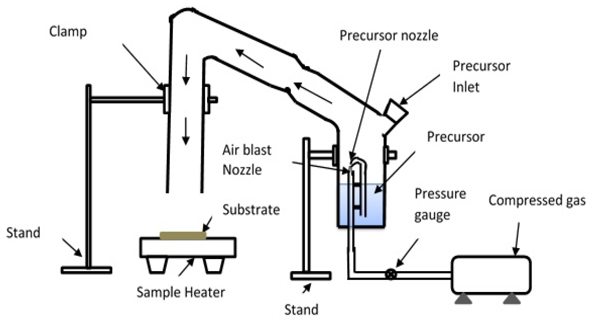
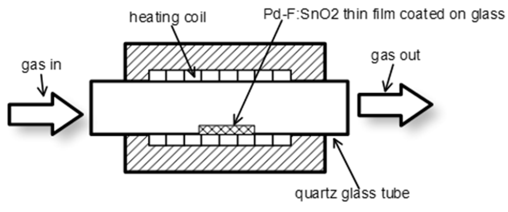
2.2. Thin Film Deposition

Spray pyrolysis technique was used to coat the films. The experimental set up used is a home-made spray pyrolysis system schematic shown in Figure 1. It consisted of a fume chamber, hot plate, spray nozzle of diameter ~1 mm, input gas valve, gas compressor, gas flow meter, conduit tube, thermocouple and a pressure gauge. Table 1 contains the deposition parameters.
Figure 1. Spray pyrolysis experimental set up.
Coatings 04 00747 g001
Table 1. Optimized deposition parameters.
S/NDeposition parametersOptimized condition
1Pressure of carrier gas1.5 bar
2Substrate temperature450 ± 10 °C
3Flow rate4 mL/min
4Quantity of spraying solution30 cm3
5Nozzle to substrate distant33 ± 3 cm
The undoped SnO2 thin films were deposited using a precursor solution consisting of Tin (IV) chloride (98%) prepared by completely dissolving 5 g of stannic chloride in 100 mL of ethanol (99.9%). 0.5 g of PdCl2 (59%–60% Pd) was completely dissolved in 60 mL of ethanol (99.9%). It was then added to stannic chloride solution at different doping concentrations ranging 1.8 at%–6.9 at% Pd. The Pd-F:SnO2 thin films were deposited using spray pyrolysis technique using similar precursor prepared as follows: ammonium fluoride was added to solution containing stannic chloride and 2.7 at% Pd at varying doping concentrations ranging from 0 to19.28 at% F. The ammonium fluoride was prepared by adding 1.0 g of NH4F to distilled water. The precursor was then poured into the spray pyrolysis equipment and deposited at 450 °C substrate temperature. The thickness of the thin films was controlled using a constant quantity of the spraying solution and was maintained in the range of 186.55 nm ±10 nm for all undoped and doped SnO2 thin films.

2.3. Thin Film Annealing

Thin films were annealed in a tube furnace (schematic diagram shown in Figure 2), in the presence of air at 450 °C for 30 min. This was done in order to harden and sinter the coatings to improve stability of the thin films. Apart from hardening and sintering the coatings, annealing was done in order to improve on the electrical conductivity of Pd-F:SnO2 thin films.
Figure 2. Tube furnace used in passivation of Pd-F:SnO2 thin films.
Coatings 04 00747 g002

2.4. Thin Film Passivation

Thin films were passivated by annealing them in a nitrogen atmosphere for 30 min at 450 °C. Since passivation is known to improve on the stability of doped SnO2 thin films [13,14,15,21], it was done in order to study its effect on electrical resistivity of Pd-F:SnO2 thin films.

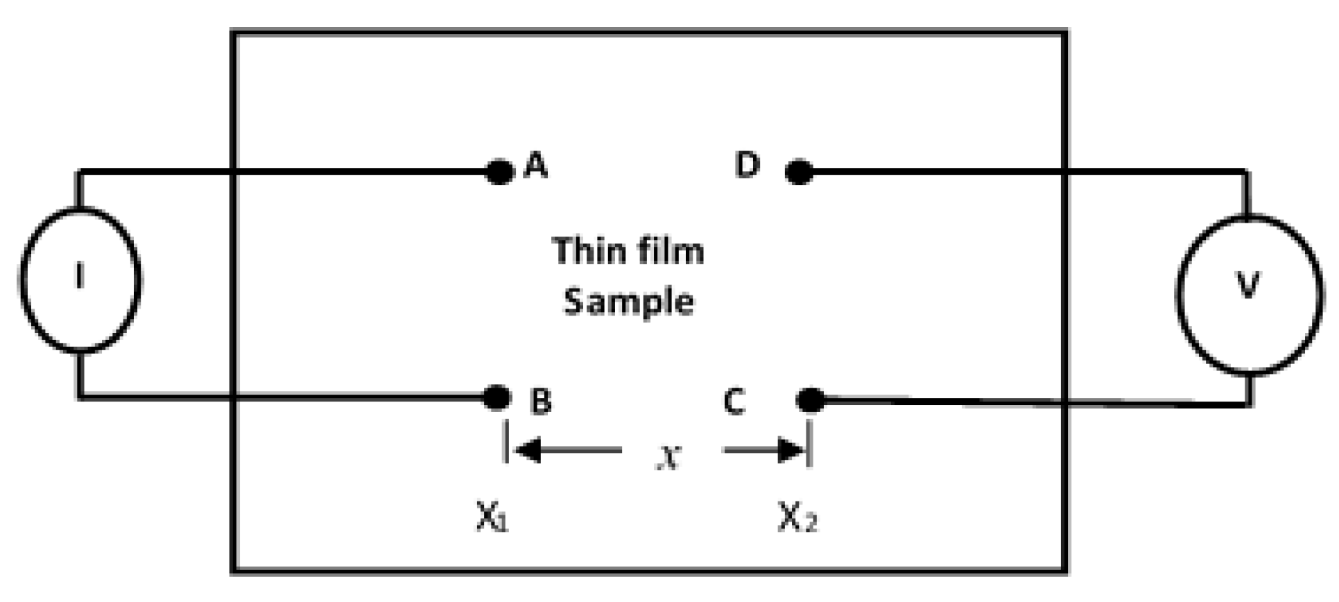
2.5. Electrical Characterization

Electrical characterization of thin films was done using the four point probe method at room temperature (25 °C). The measurements were taken in a square geometry using Keithley 2400 Source Meter (Keithly, Cleveland, OH, USA). The four contact terminals of Keithley 2400 Source Meter were placed on the surface of the thin film as shown in Figure 3. Typical probe spacing X1–X2 is about 20 mm.
A high impedance current source was used to supply current through the two probes A and B and a voltmeter was used to measure the voltage across probes C and D as shown in Figure 3. The values of sourced current and measured voltages were used to determining the sample resistivity using Equation 1.
ρ s = β ( V I ) t
where β is a geometric factor and in the case of a semi-infinite thin sheet, β = 4.53, which is just π/ln 2 from the derivation of Equation 1 and t, is the simulated thickness of the thin films which was determined using Scout 98™ software [8,23].
Figure 3. A schematic diagram showing the four points configuration used in making electrical measurements.
Coatings 04 00747 g003

3. Results and Discussion

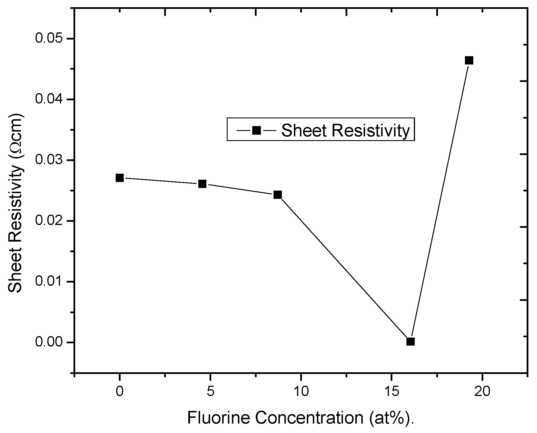
3.1. Sheet Resistivity

Figure 4 shows sheet resistivity obtained for undoped and palladium doped SnO2 thin films at various doping level. Undoped SnO2 thin films had a low sheet resistivity of 5.992 × 10⁻¹ Ω cm which can be attributed to deviation from stoichiometry due to creation of oxygen vacancies which act like electron donors and increase free carrier concentration [11,24].
Figure 4. Sheet resistivity characteristics of Pd:SnO2.
Coatings 04 00747 g004
Initially, as the dopant concentration was increased, the sheet resistivity decreased up to a minimum value. Different doped SnO2 thin films were measured which had different level of palladium doping from 0 at% Pd to 6.9 at% Pd. The graph in Figure 4 shows gradual decrease till a minima at 2.7 at% Pd doping in Pd:SnO2 thin film which correspondingly gave the least sheet resistivity of about 2.71 × 10⁻² Ω cm. The decrease in sheet resistivity can be attributed to the presence of palladium ions in the crystal lattice of SnO2 which contributes more electrons into the lattice hence the increase in free carrier concentration. After the minimum point, increasing the dopant concentration above the optimum value of doping, the sheet resistivity of the thin films increases almost proportionately. This is because palladium atoms incorporate themselves in the interstitial sites of the thin film and the crystal structure begins to deteriorate causing a decrease in mobility of free charge carriers hence the increase in sheet resistivity of the thin films [20].
The effect of fluorine incorporation in Pd:SnO2 thin film was then studied using thin film based on optimum doping of Pd:SnO2. Figure 5 shows sheet resistivity results obtained for Pd-F:SnO2 thin films at different at% of fluorine. Increase in fluorine concentration from 0 at% F to 16.04 at% F led to a decrease in sheet resistivity from 2.71 × 10⁻² to 1.64 × 10⁻⁴ Ω cm. The decrease in sheet resistivity can be attributed to substitutional incorporation of F-ions in the crystal lattice of Pd:SnO2 thin films instead of O ions leading to increase in free carrier concentration [20].
Figure 5. Sheet resistivity characteristics of Pd-F:SnO2.
Coatings 04 00747 g005
The Pd-F:SnO2 thin films with the least sheet resistivity was obtained at 16.04 at% F. Upon increasing the dopant concentration above the optimum level of doping, the sheet resistivity increased again. This is attributed to deterioration of the crystal structure hence decreasing the mobility of the free electrons which lead to an increase in the sheet resistivity of the thin films [20].

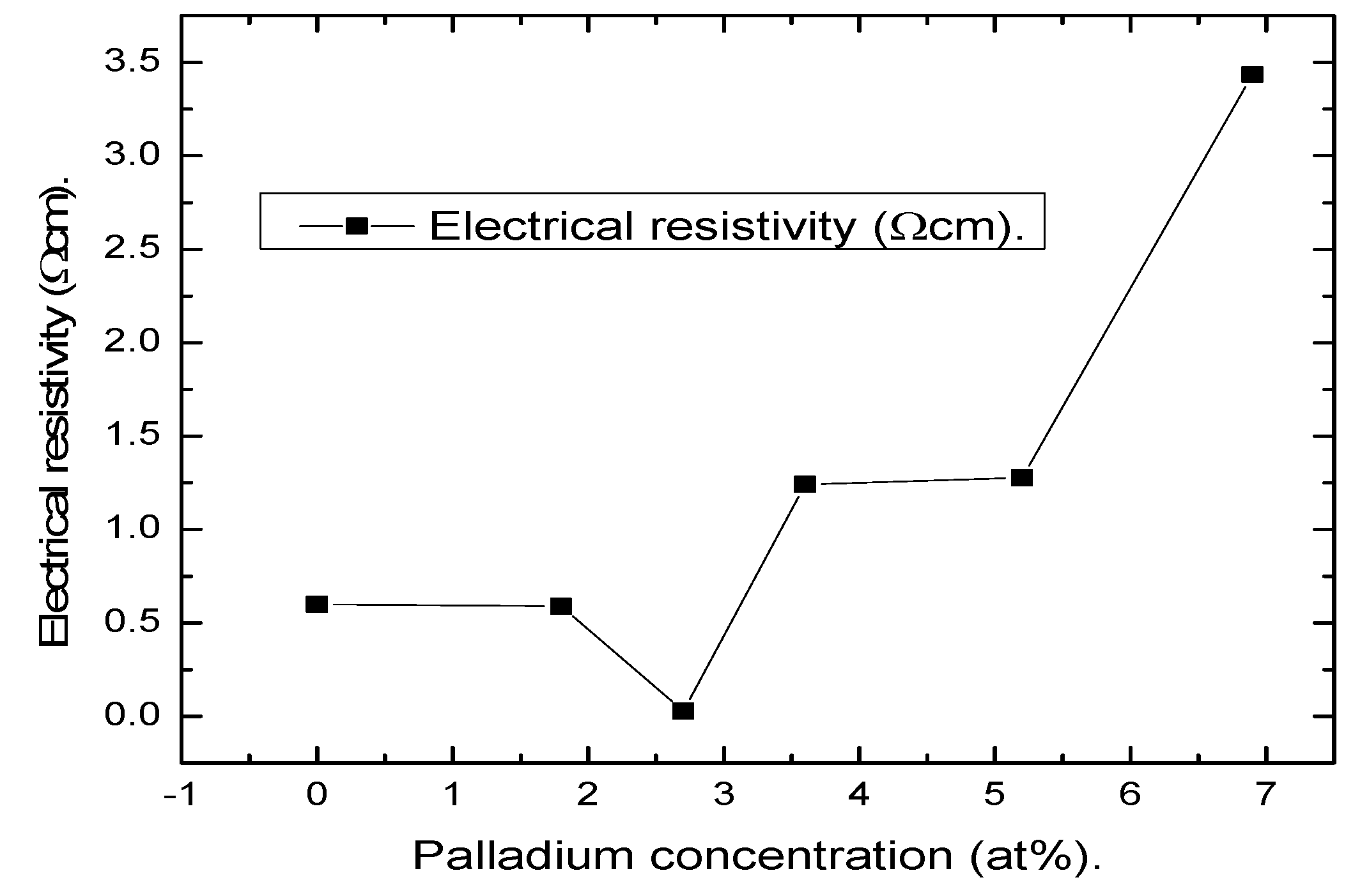
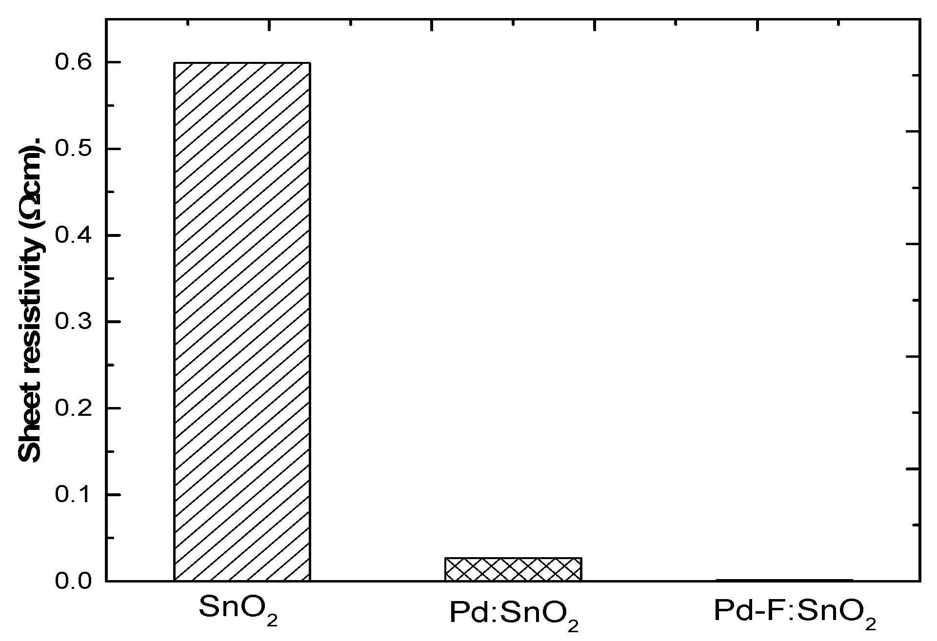
3.2. Comparison of Doped Thin Films

Figure 6 shows a comparison on the sheet resistivity of SnO2 based thin films prepared under optimized doping concentrations. Sheet resistivity of 5.992 × 10⁻¹ Ω cm was recorded for SnO2 thin films. This low sheet resistivity can be attributed to the formation of Fermi levels in the conduction band of SnO2 thin films [11].
Figure 6. Sheet resistivity characteristics of SnO2, Pd:SnO2 and Pd-F:SnO2 thin films.
Coatings 04 00747 g006
From Figure 6, the sheet resistivity of SnO2 thin film decreases significantly when SnO2 is doped with palladium at optimum condition (2.7 at% Pd) from 5.992 × 10⁻¹ to 2.71 × 10⁻² Ω cm. A similar decrease is observed when fluorine is added to Pd:SnO2, the resistivity decreases from 2.71 × 10⁻² to 1.64 × 10⁻⁴ Ω cm for 16.04 at% F.

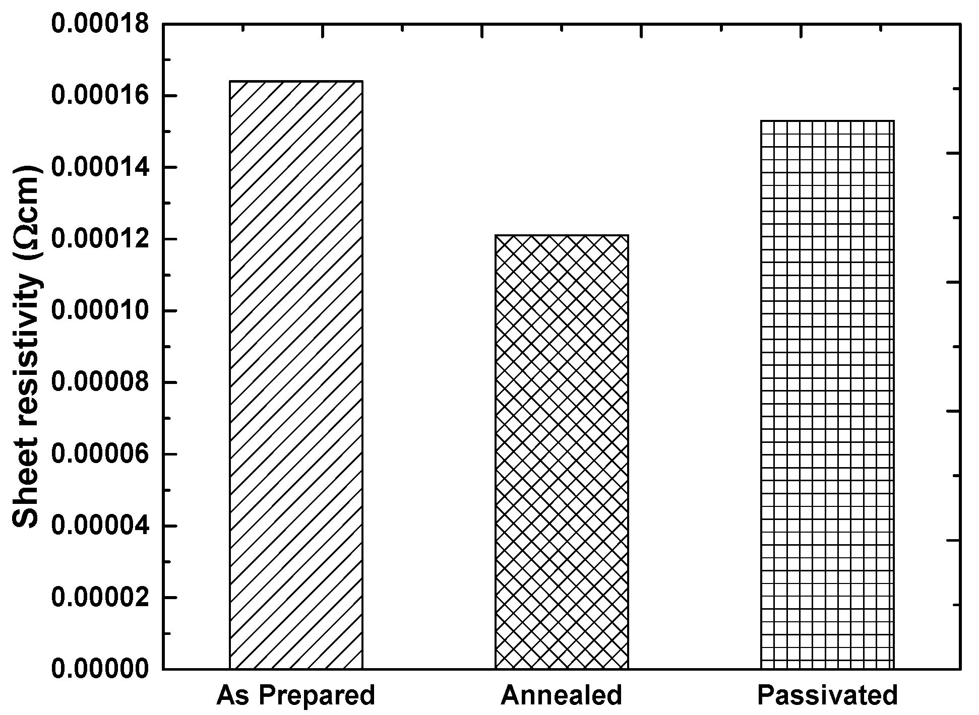
3.3. Post Deposition Treatment of Pd-F:SnO2 Thin Films

From Figure 7, sheet resistivity of Pd-F:SnO2 thin films decreased from 1.64 × 10⁻⁴ to 1.21 × 10⁻⁴ Ω cm upon annealing in air. The decrease in sheet resistivity of the thin films can be attributed to an increase in crystallinity of the thin films hence increase in mobility and carrier density [18]. Passivating the annealed thin films led to an increase in the sheet resistivity from 1.21 × 10⁻⁴ to 1.53 × 10⁻⁴ Ω cm. This can be attributed to the effects of annealing the samples in oxygen deficient atmosphere (nitrogen) [19].
Figure 7. Sheet resistivity comparison for as prepared, annealed and passivated Pd-F:SnO2 thin films.
Coatings 04 00747 g007

4. Conclusions

The SnO2 thin films have been found to have resistivity of about 5.992 × 10⁻¹ Ω cm; this low resistivity has been attributed to deviation from stoichiometry and creation of oxygen vacancies. On doping the SnO2 with palladium, the sheet resistivity of Pd:SnO2 has been observed to decrease due to the presence of Pd ions into the crystal lattice which contributes more electron ions into the lattice increasing electron carriers. Further doping with Pd sheet resistivity starts to increase, this behavior has been attributed to formation of Pd ions in the interstitial sites of the lattice hence change in structure of the films and therefore decreasing the number of free charge carriers. When Pd:SnO2 is doped with fluorine, sheet resistivity lower than that of 2.7 at% Pd:SnO2 is observed. This is due to the substitutional incorporation of F-ions in crystal lattice of Pd:SnO2 instead of O- ions leading to increase in free carrier concentration, further doping sees the onset of increase in sheet resistivity due to decrease of free electron carriers. This type of thin film can find good application as gas sensor. Annealing of Pd-F:SnO2 sheet resistivity decreases due to increased mobility and carrier density, while, when the same type of thin film is passivated, the effect of annealing the samples in a nitrogen gas atmosphere contributes to the increment in sheet resistivity.

Acknowledgments

The authors of this paper would wish to acknowledge the technical staff of both Nairobi and Kenyatta University in Particular Everyline Akinyi and Abraham Chisaina for their technical advice while carrying out the experiments in the Laboratory.

Author Contributions

Patrick Mwathe, Robinson Musembi and Mathew Munji conceived and designed the experiments; Patrick Mwathe performed the experiments, analyzed the data and wrote the paper together with Robinson Musembi; Mathew Munji, Victor Odari, Lawrence Munguti, Alex Ntilakigwa and John Nguu assisted in giving the paper a scientific outlook; Boniface Muthoka and Victor Odari gave technical advice while handling depositions and measurements.

Conflicts of Interest

The authors declare no conflict of interest.

References

  1. Young, S.K.; Ansari, S.G.; Ansari, Z.A.; Rizwan, W.; Hyung-Shik, S. A simple method to deposit palladium doped SnO2 thin films using plasma enhanced chemical vapor deposition technique. Rev. Sci. Instrum. 2010, 81. [Google Scholar] [CrossRef]
  2. Chowdhury, F.R.; Chowdhury, S.; Hasan, F.; Begum, T. Optical properties of undoped and indium doped tin oxide thin films. J. Bangladesh Acad. Sci. 2011, 35, 99–111. [Google Scholar] [CrossRef]
  3. Salehi, H.; Aryadoust, M.; Farbod, M. Electronic and structural properties of tin dioxide in cubic phase. Iran. J. Sci. Technol. Trans. A 2010, 34, 131–138. [Google Scholar]
  4. Ikhmayies, S.J.; Ahmad-Bitar, R.N. Effect of processing on the electrical properties of spray-deposited SnO2:F thin films. Am. J. Appl. Sci. 2008, 5, 672–677. [Google Scholar] [CrossRef]
  5. Mishra, R.L.; Mishra, S.K.; Prakash, S.G. Optical and gas sensing characteristics of tin-dioxide nano-crystalline thin films. J. Ovonic Res. 2009, 5, 77–85. [Google Scholar]
  6. Díaz, R. Tin oxide thin films: Electronic properties and growth mechanism under electrochemical control. Ph.D. Thesis, University of Barcelona, Barcelona, Spain, 2002. [Google Scholar]
  7. Shamala, K.S.; Murthy, L.C.S.; Rao, K.N. Studies on tin oxide films prepared by electron beam evaporation and spray pyrolysis methods. Bull. Mater. Sci. 2004, 27, 295–301. [Google Scholar] [CrossRef]
  8. Jebbari, N.; Kamoun, N.; Bennaceur, R. Effect of SnCl4 concentration on F:SnO2, deposited by chemical spray pyrolysis. In the Proceedings of International Renewable Energy Congress, Souse, Tunisia, 5–7 November 2010; pp. 276–279.
  9. Yousaf, S.A.; Ali, S. The effect of fluorine doping on optoelectronic properties of tin-dioxide (F:SnO2) thin films. Coden. Jnsmac. 2008, 48, 43–50. [Google Scholar]
  10. Odari, B.V.; Musembi, R.J.; Mageto, M.J.; Othieno, H.; Gaitho, F.; Mghendi, M.; Muramba, V. Optoelectronic properties of F-co-doped PTO thin films deposited by spray pyrolysis. Am. J. Mater. Sci. 2013, 3, 91–99. [Google Scholar] [CrossRef]
  11. Baco, S.; Chik, A.; Tassin, F.Md. Study on optical properties of tin oxide thin films at different annealing temperatures. J. Sci. Technol. 2012, 4, 61–72. [Google Scholar]
  12. Miller, T.A.; Bakrania, S.D.; Perez, C.; Woondridge, M.S. Nanostructured Tin Dioxide Materials for Gas Sensor Applications; American Scientific Publishers: Valencia, CA, USA, 2006; pp. 1–24. [Google Scholar]
  13. Bochenkov, V.E.; Sergeev, G.B. Sensitivity, Selectivity, and Stability of Gas-Sensitive Metal-Oxide Nanostructures and Their Applications; American Scientific Publishers: Valencia, CA, USA, 2010; pp. 31–52. [Google Scholar]
  14. Vaezi, M.R. Effects of surface modification on the recovery time and stability of nano structured tin oxide thick films gas sensors. Int. J. Electron. Trans. B Appl. 2007, 20, 1–8. [Google Scholar]
  15. Adamyan, A.Z.; Adamyan, Z.N.; Aroutiounian, V.M.; Schietbaum, K.D.; Han, S.-D. Improvement and stabilization of thin-film hydrogen sensors parameters. Am. J. Phys. 2009, 2, 200–212. [Google Scholar]
  16. De Moure-Flores, F.; Guillen-Gervauntes, A.; Nieto-Zapeda, K.E.; Quinones-Galvan, J.G.; Hernandez-Hernandez, A.; Olvera, M.G.; Melendez-Lira, M. SnO2 thin films deposited by RF magnetron sputtering: Effect of the SnF2 amount in the target on the physical properties. Rev. Mex. Fis. 2013, 59, 335–338. [Google Scholar]
  17. Al-Delaimy, S.M.; Basheer, R.J. Annealing effects on structural and optcal properties of SnO2 thin films. J. Edu. Sci. 2008, 21, 99–109. [Google Scholar]
  18. Senthilkumara, V.; Vickramana, P.; Joseph Princeb, J.; Jayachandranc, M.; Sanjeevirajad, C. Effects of annealing temperature on structural, optical, and electrical properties of antimony-doped tin oxide thin films. Philos. Mag. Lett. 2010, 90, 337–347. [Google Scholar] [CrossRef]
  19. Jain, V.K.; Kumar, P.; Vijay, Y.K. Preparation of nanostructure ZnO-SnO2 thin films for optoelectronic properties and post annealing influence. World Acad. Sci. Eng. Technol. 2012, 72, 1575–1577. [Google Scholar]
  20. Yadav, A.A.; Masumdar, E.U.; Moholkar, A.V.; Rajpure, K.Y.; Bhosale, C.H. Gas sensing of fluorine doped tin oxide thin films prepared by spray pyrolysis. J. Sens. Transducers 2008, 92, 55–60. [Google Scholar]
  21. Radecka, M.; Zakrzewska, K.; Rekas, M. SnO2-TiO2 solid solutions for gas sensors. Sens. Actuators B 1998, 47, 194–204. [Google Scholar] [CrossRef]
  22. Ozaki, Y.; Suzuki, S.; Morimitsu, M.; Matsunaga, M. Enhanced long-term stability of SnO2-based CO gas sensors modified by sulfuric acid treatment. Sens. Actuators B 2000, 62, 220–225. [Google Scholar] [CrossRef]
  23. Scout Thin Film Analysis Software Handbook. W.Theiss Hard- and Software Website. Available online: http://www.wtheiss.com/ (accessed on 14 November 2014).
  24. Mohammad, T.M. Performance and characteristics of Al-PbS/SnO2: F selective coating system for photothermal energy conversion. Solar Energy Mater. 1990, 20, 297–305. [Google Scholar] [CrossRef]

