
Role of Cl on Diffusion of Cu in In2S3 Layers Prepared by Ion Layer Gas Reaction Method

Abstract
:1. Introduction
2. Experimental Section
3. Results and Discussion

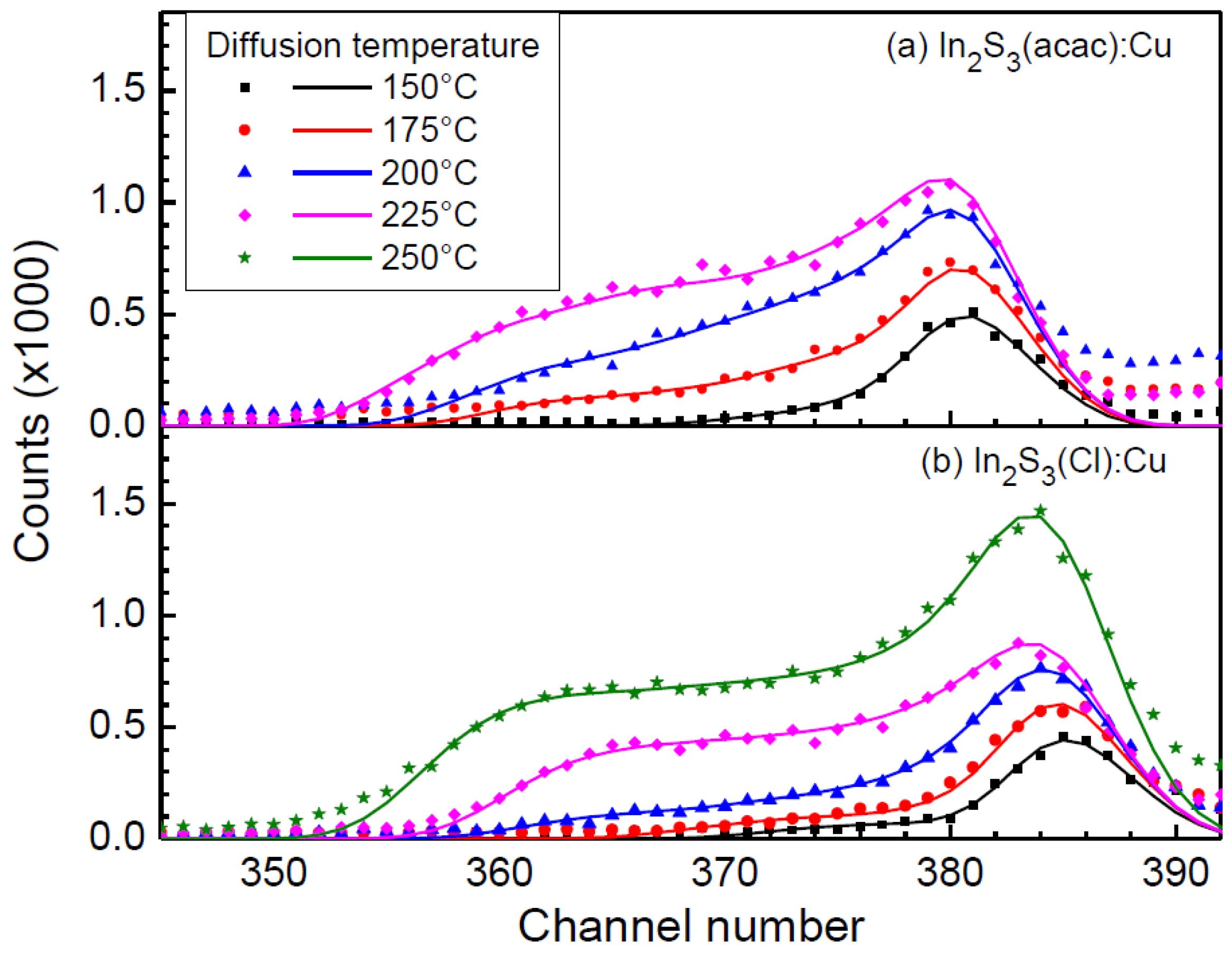
| Name | Thickness (nm) | In (at.%) | S (at.%) | Cl (at.%) | S/In |
|---|---|---|---|---|---|
| S0 | 86 | 39 | 61 | 0 | 1.56 |
| S8 | 152 | 37.5 | 52.2 | 11.3 | 1.41 |
| S9 | 65 | 37.1 | 49.1 | 13.8 | 1.32 |
| S11 | 64 | 37.8 | 54.4 | 7.8 | 1.44 |
| S12 | 45 | 37.6 | 53.9 | 8.6 | 1.43 |


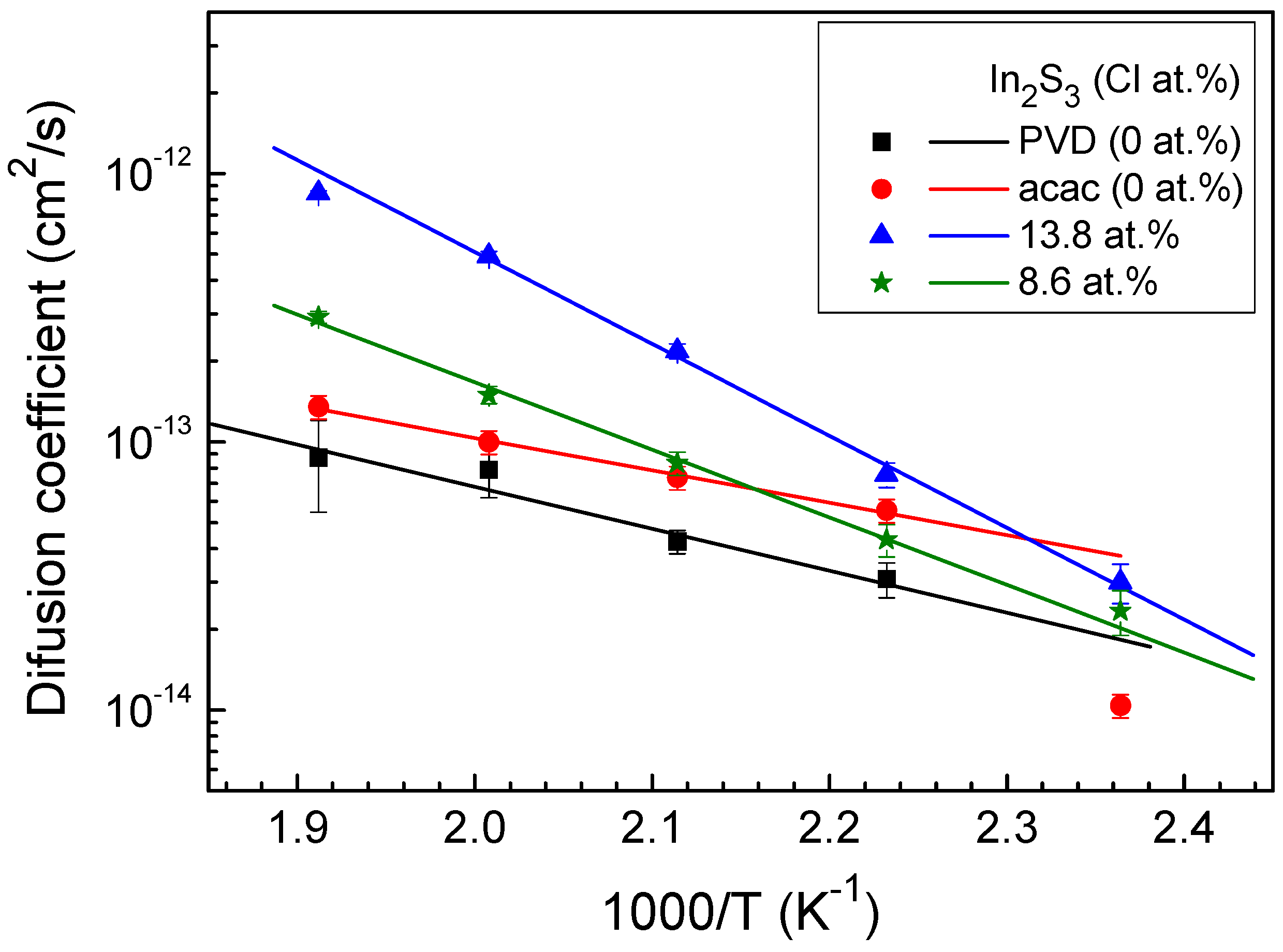
| In2S3 films | Activation energy EA (eV) | Exponential prefactor D0 (cm2/s) |
|---|---|---|
| In2S3:Cl 13.8 at.% | 0.70 | 6.0 × 10⁻⁶ |
| In2S3:Cl 11.3 at.% | 0.72 | 3.0 × 10⁻⁶ |
| In2S3:Cl 8.5 at.% | 0.78 | 3.2 × 10⁻⁵ |
| In2S3:Cl 7.8 at.% | 0.76 | 1.2 × 10⁻⁵ |
| In2S3:acac | 0.24 | 2.7 × 10⁻¹¹ |
| In2S3:PVD | 0.30 | 9.0 × 10⁻¹¹ |
4. Conclusions
Acknowledgments
Author Contributions
Conflicts of Interest
References
- Barreau, N.; Bernéde, J.C.; El Maliki, H.; Marsillac, S.; Castel, X.; Pinel, J. Recent studies on In2S3 containing oxygen thin films. Solid State Commun. 2002, 122, 445–450. [Google Scholar] [CrossRef]
- Bär, M.; Allsop, N.; Lauermann, I.; Fischer, C.-H. Deposition of In2S3 on Cu(In,Ga)(S,Se)2 thin film solar cell absorbers by spray ion layer gas reaction: Evidence of strong interfacial diffusion. Appl. Phys. Lett. 2007, 90. [Google Scholar] [CrossRef]
- Abou-Ras, D.; Kostorz, G.; Strohm, A.; Schock, H.-W.; Tiwari, A.N. Interfacial layer formations between Cu(In, Ga)Se2 and InxSy layers. J. Appl. Phys. 2005, 98. [Google Scholar] [CrossRef]
- Barreau, N. Indium sulfide and relatives in the world of photovoltaics. Sol. Energy 2009, 83, 363–371. [Google Scholar] [CrossRef]
- Nanu, M.; Schoonman, J.; Goossens, A. Nanocomposite three-dimensional solar cells obtained by chemical spray deposition. Nano Lett. 2005, 5, 1716–1719. [Google Scholar] [CrossRef] [PubMed]
- Nanu, M.; Schoonman, J.; Goossens, A. Inorganic nanocomposites of n- and p-type semiconductors: A new type of three-dimensional solar cell. Adv. Mater. 2004, 16, 453–456. [Google Scholar] [CrossRef]
- Belaidi, A.; Dittrich, T.; Kieven, D.; Tornow, J.; Schwarzburg, K.; Kunst, M.; Allsop, N.; Lux-Steiner, M.-C.; Gavrilov, S. ZnO-nanorod arrays for solar cells with extremely thin sulfidic absorber. Sol. Energy Mater. Sol. Cells 2009, 93, 1033–1036. [Google Scholar] [CrossRef]
- Kieven, D.; Dittrich, T.; Belaidi, A.; Tornow, J.; Schwarzburg, K.; Allsop, N.; Lux-Steiner, M. Effect of internal surface area on the performance of ZnO/In2S3/CuSCN solar cells with extremely thin absorber. Appl. Phys. Lett. 2008, 92. [Google Scholar] [CrossRef]
- Herzog, C.; Belaidi, A.; Ogacho, A.; Dittrich, T. Inorganic solid state solar cell with ultra-thin nanocomposite absorber based on nanoporous TiO2 and In2S3. Energy Environ. Sci. 2009, 2, 962–964. [Google Scholar] [CrossRef]
- Abou-Ras, D.; Rudmann, D.; Kostorz, G.; Spiering, S.; Powalla, M.; Tiwari, A.N. Microstructural and chemical and studies of interfaces between Cu(In,Ga)Se2 and In2S3 layers. J. Appl. Phys. 2005, 97. [Google Scholar] [CrossRef]
- Pistor, P.; Allsop, N.; Braun, W.; Caballero, R.; Camus, C.; Fischer, C.-H.; Gorgoi, M.; Grimm, A.; Johnson, B.; Kropp, T.; et al. Cu in In2S3: Interdiffusion phenomena analysed by high kinetic energy X-ray photoelectron spectroscopy. Phys. Status Solidi A 2009, 206, 1059–1062. [Google Scholar]
- Dittrich, T.; Kieven, D.; Belaidi, A.; Rusu, M.; Tornow, J.; Schwarzburg, K.; Lux-Steiner, M.C. Formation of the charge selective contact in solar cells with extremely thin absorber based on ZnO-nanorod/In2S3/CuSCN. J. Appl. Phys. 2009, 105. [Google Scholar] [CrossRef]
- Rooyman, C.J.M. A new type of cation-vacancy ordering in the spinel lattice of In2S3. J. Inorg. Nucl. Chem. 1959, 11, 78–79. [Google Scholar] [CrossRef]
- King, G.S.D. The space group of β-In2S3. Acta Cryst. 1962, 15, 512. [Google Scholar] [CrossRef]
- Hahn, H.; Klinger, W. The crystal structures of the In2S3 and In2Te3. Z. Anorg. Chem. 1949, 260, 97–109. [Google Scholar] [CrossRef]
- Diehl, R.; Carpentier, C.-D.; Nitsche, R. The crystal structure of γ-In2S3 stabilized by As or Sb. Acta Cryst. 1976, B32, 1257–1260. [Google Scholar] [CrossRef]
- Diehl, R.; Nitsche, R. Vapour growth of three In2S3 modifications by iodine transport. J. Cryst. Growth 1975, 28, 306–310. [Google Scholar] [CrossRef]
- Womes, M.; Olivier-Fourcade, J.; Jumas, J.-C.; Aubertin, F.; Gonser, U. Characterization of the single phase region with spinel structure in the ternary system In2S3-FeS-FeS2. J. Solid State Chem. 1992, 97, 249–256. [Google Scholar] [CrossRef]
- Mathew, M.; Sudha Kartha, C.; Vijayakumar, K.P. In2S3:Ag, an ideal buffer layer for thin film solar cells. J. Mater. Sci. Mater. Electron. 2009, 20, 294–298. [Google Scholar] [CrossRef]
- Cherian, A.S.; Mathew, M.; Kartha, C.S.; Vijayakumar, K.P. Role of chlorine on the opto-electronic properties of β-In2S3 thin films. Thin Solid Films 2010, 518, 1779–1783. [Google Scholar] [CrossRef]
- Guillot-Deudon, C.; Harel, S.; Mokrani, A.; Lafond, A.; Barreau, N.; Fernandez, V.; Kessler, J. Electronic structure of NaxCu1−xIn5S8 compounds: X-ray photo emission spectroscopy study and band structure calculations. Phys. Rev. B 2008, 78. [Google Scholar] [CrossRef]
- Py, F.; Womes, M.; Durand, J.M.; Olivier-Fourcade, J.; Jumas, J.-C.; Esteva, J.M.; Karnatak, R.C. Copper in In2S3: A study by X-ray diffraction, diffuse reflectance and X-ray absorption. J. Alloys Compd. 1992, 178, 297–304. [Google Scholar] [CrossRef]
- Juma, A.O.; Pistor, P.; Fengler, S.; Dittrich, T.; Wendler, E. Copper diffusion in thin In2S3 layers investigated by Rutherford Backscattering spectroscopy. Thin Solid Films 2012, 520, 6740–6743. [Google Scholar] [CrossRef]
- Fischer, C.-H.; Muffler, H.-J.; Bär, M.; Fiechter, S.; Leupolt, B.; Lux-Steiner, M.C. Ion layer gas Reaction (ILGAR)-conversion thermodynamic considerations and related FTIR analysis. J. Cryst. Growth 2002, 241, 151–158. [Google Scholar] [CrossRef]
- Gledhill, S.; Allison, R.; Allsop, N.; Fu, Y.; Kanaki, E.; Sáez-Araoz, R.; Lux-Steiner, M.; Fischer, C.-H. The reaction mechanism of the spray ion layer Gas reaction process to deposit In2S3 thin films. Thin Solid Films. 2011, 519, 6413–6419. [Google Scholar] [CrossRef]
- Sáez-Araoz, R.; Krammer, J.; Harndt, S.; Koehler, T.; Krueger, M.; Pistor, P.; Jasenek, A.; Hergert, F.; Lux-Steiner, M.C.; Fischer, C.-H. ILGAR In2S3 buffer layers for Cd-free Cu(In,Ga)(S,Se)2 solar cells with certified efficiencies above 16%. Prog. Photovolt. Res. Appl. 2012, 20, 855–861. [Google Scholar] [CrossRef]
- Jeynes, C.; Barradas, N.P.; Szilágyi, E. Accurate determination of quantity of material in thin films by rutherford backscattering spectrometry. Anal. Chem. 2012, 84, 6061–6069. [Google Scholar] [CrossRef] [PubMed]
- Jeynes, C.; Barradas, N.P.; Rafla-Yuan, H.; Hichwa, B.P.; Close, R. Accurate depth profiling of complex optical coatings. Surf. Interface Anal. 2000, 30, 237–242. [Google Scholar] [CrossRef]
- Kumara, G.R.R.A.; Konno, A.; Senadeera, G.K.R.; Jayaweera, P.V.V.; de Silva, D.B.R.A.; Tennakone, K. Dye-sensitized solar cell with the hole collector p-CuSCN deposited from a solution in-propyl Sulphide. Sol. Energy Mater. Sol. Cells 2001, 69, 195–199. [Google Scholar] [CrossRef]
- Barradas, N.P.; Jeynes, C.; Webb, R.P. Simulated annealing analysis of Rutherford backscattering data. Appl. Phys. Lett. 1997, 71. [Google Scholar] [CrossRef]
- Juma, A.O.; Azarpira, A.; Steigert, A.; Pomaska, M.; Fischer, C.-H.; Lauermann, I.; Dittrich, T. Role of chlorine in In2S3 for band alignment at nanoporous-TiO2/In2S3 Interfaces. J. Appl. Phys. 2013, 114. [Google Scholar] [CrossRef]
© 2015 by the authors; licensee MDPI, Basel, Switzerland. This article is an open access article distributed under the terms and conditions of the Creative Commons Attribution license (http://creativecommons.org/licenses/by/4.0/).
Share and Cite
Wafula, H.; Robinson, M.; Juma, A.; Sakwa, T.; Kitui, M.; Araoz, R.; Fischer, C.-H. Role of Cl on Diffusion of Cu in In2S3 Layers Prepared by Ion Layer Gas Reaction Method. Coatings 2015, 5, 54-62. https://doi.org/10.3390/coatings5010054
Wafula H, Robinson M, Juma A, Sakwa T, Kitui M, Araoz R, Fischer C-H. Role of Cl on Diffusion of Cu in In2S3 Layers Prepared by Ion Layer Gas Reaction Method. Coatings. 2015; 5(1):54-62. https://doi.org/10.3390/coatings5010054
Chicago/Turabian StyleWafula, Henry, Musembi Robinson, Albert Juma, Thomas Sakwa, Manasse Kitui, Rodrigo Araoz, and Christian-H. Fischer. 2015. "Role of Cl on Diffusion of Cu in In2S3 Layers Prepared by Ion Layer Gas Reaction Method" Coatings 5, no. 1: 54-62. https://doi.org/10.3390/coatings5010054
APA StyleWafula, H., Robinson, M., Juma, A., Sakwa, T., Kitui, M., Araoz, R., & Fischer, C.-H. (2015). Role of Cl on Diffusion of Cu in In2S3 Layers Prepared by Ion Layer Gas Reaction Method. Coatings, 5(1), 54-62. https://doi.org/10.3390/coatings5010054