
Fabrication of Efficient Cu2ZnSnS4 Solar Cells by Sputtering Single Stoichiometric Target

Abstract
:1. Introduction
2. Materials and Methods
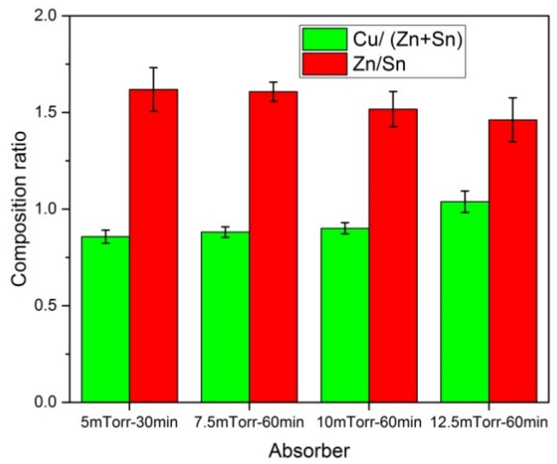
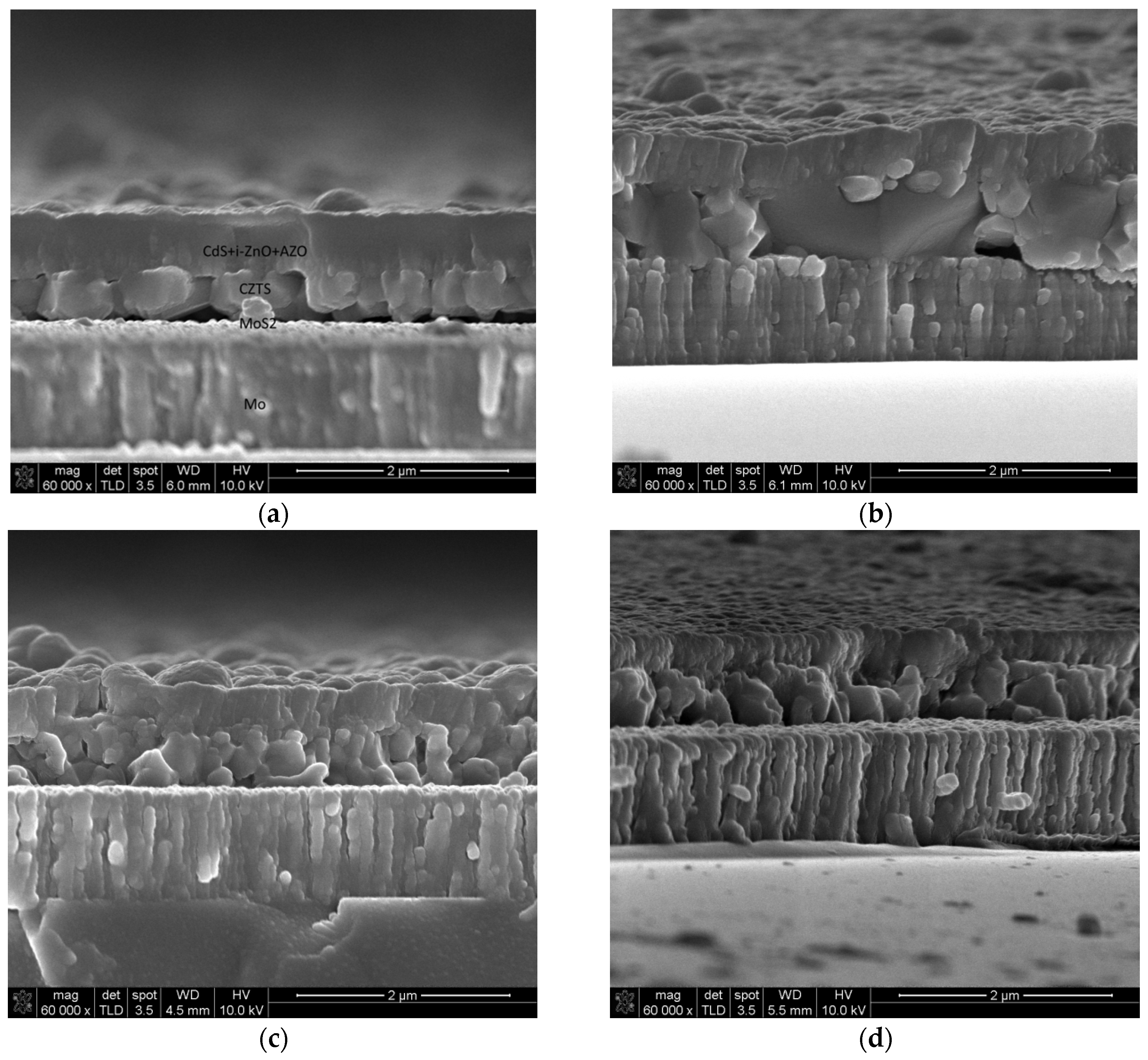
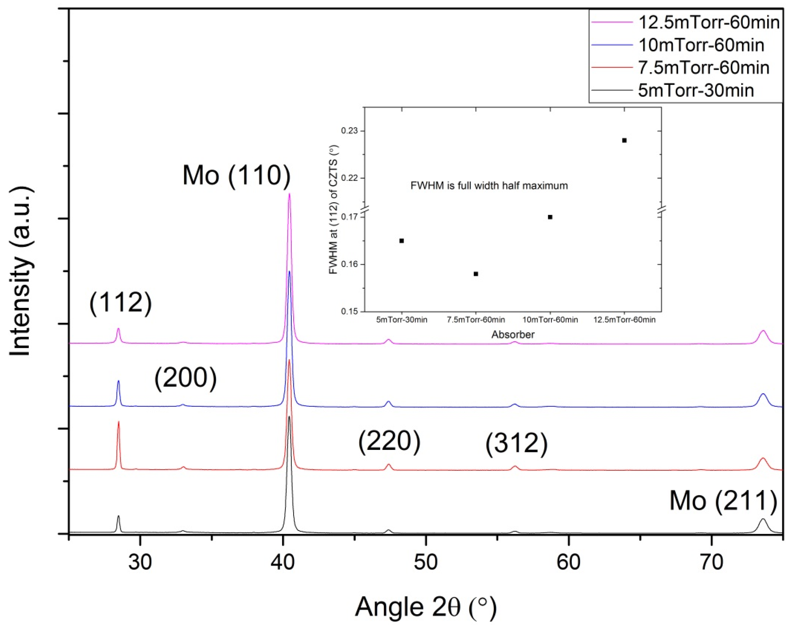
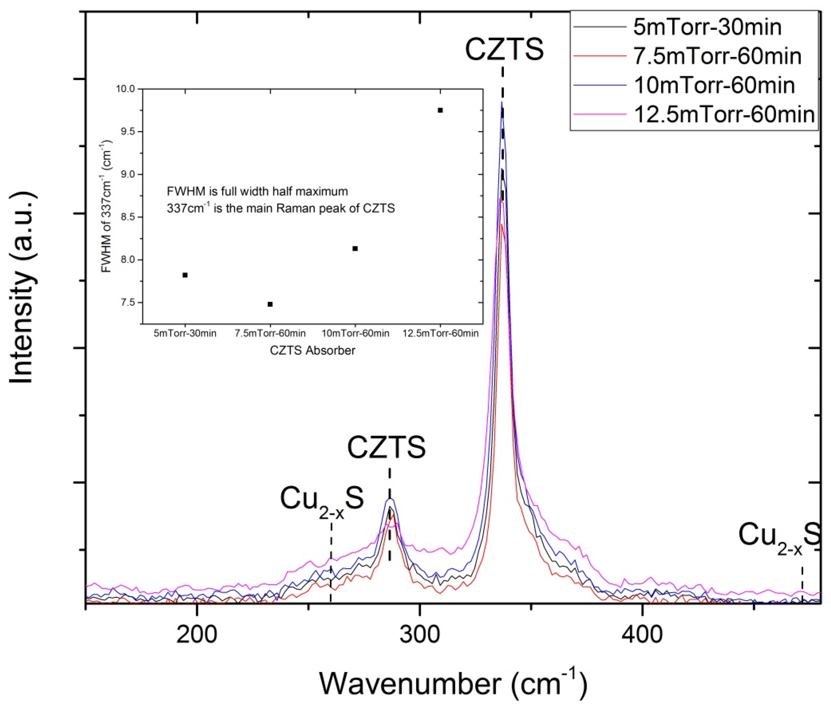
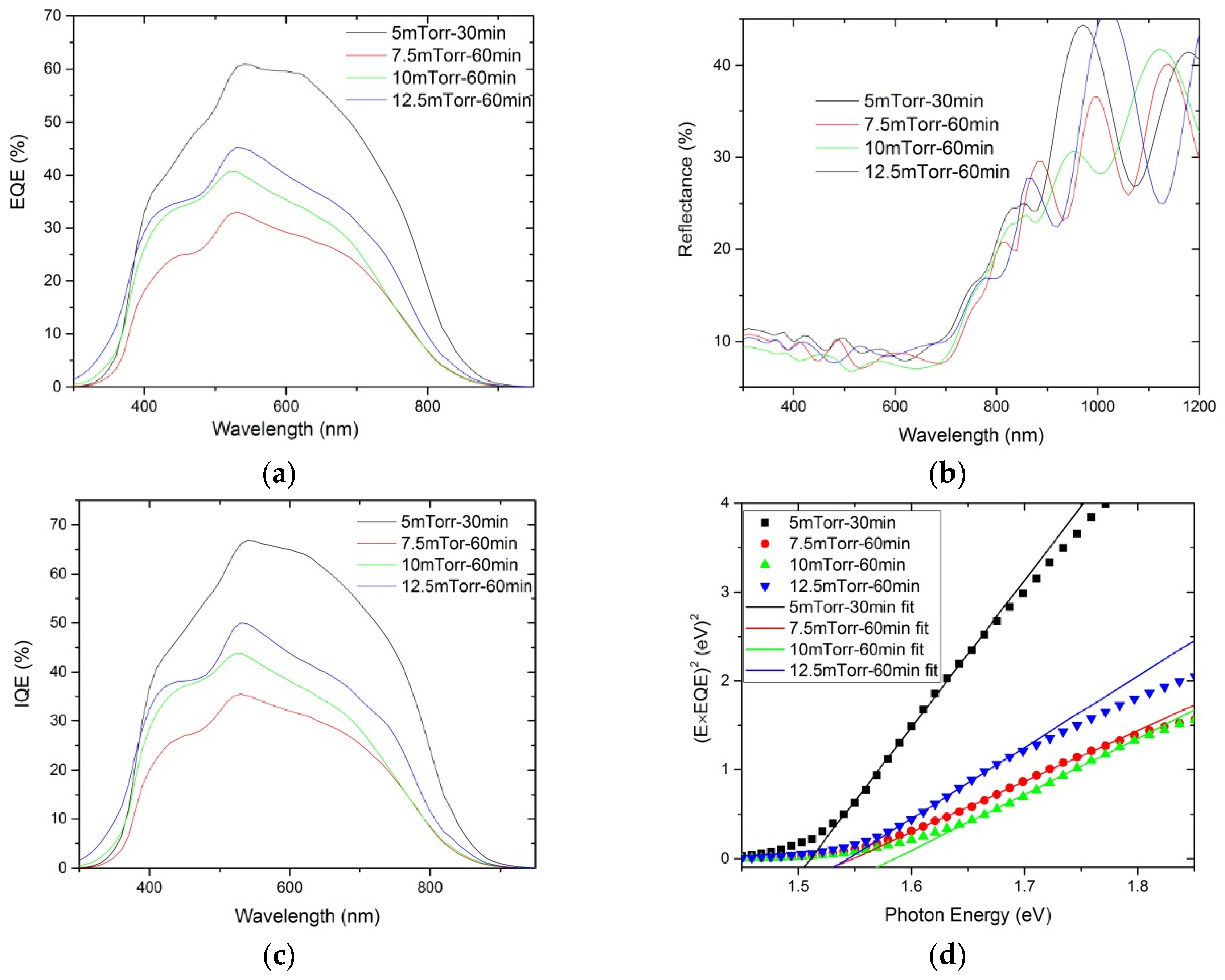
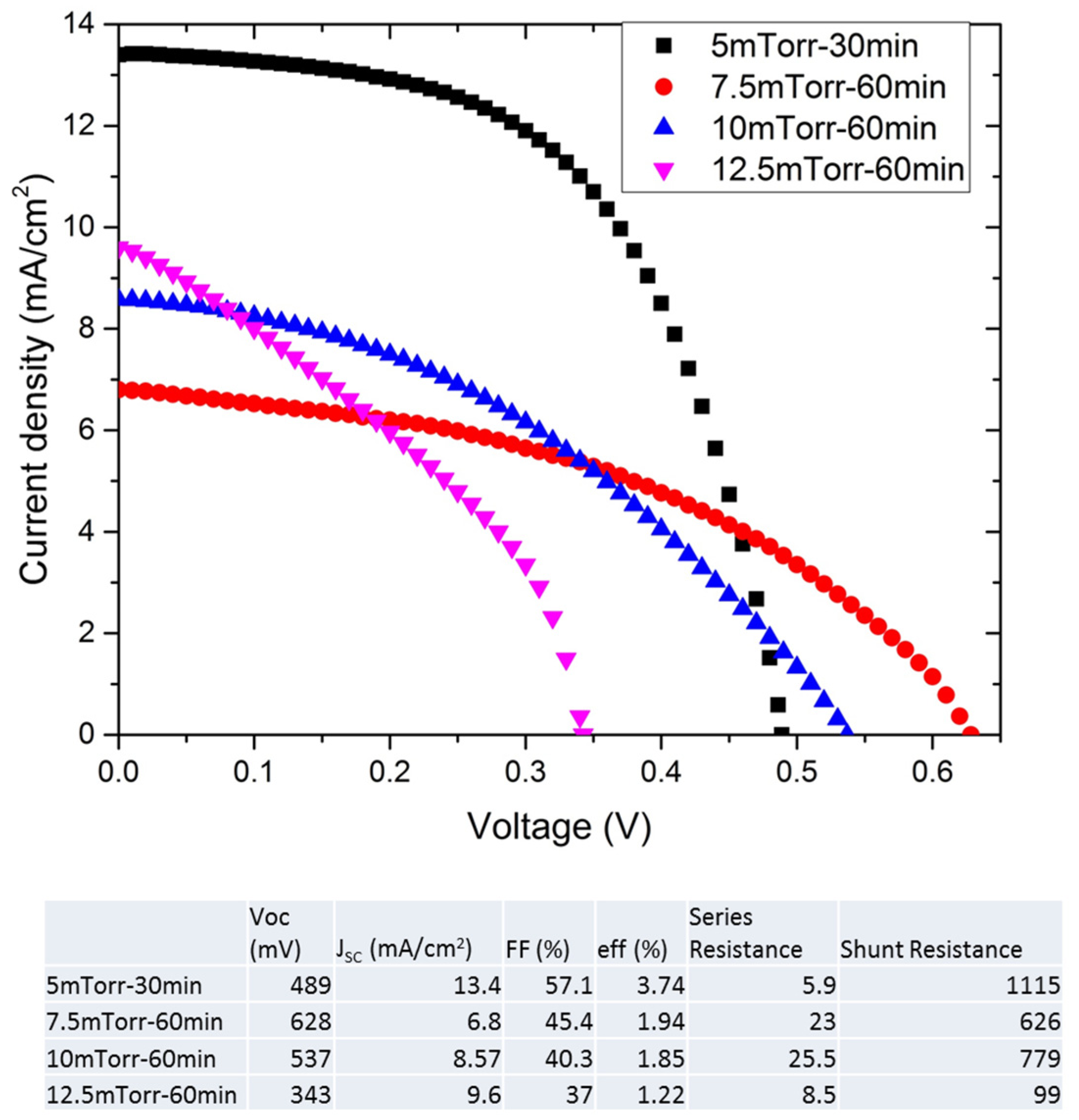
3. Results and Discussion
4. Conclusions
Acknowledgments
Author Contributions
Conflicts of Interest
References
- Peter, L.M. Towards sustainable photovoltaics: The search for new materials. Phil. Trans. R. Soc. A 2011, 369, 1840–1856. [Google Scholar] [CrossRef] [PubMed]
- Mitzi, D.B.; Gunawan, O.; Todorov, T.K.; Barkhouse, D.A.R. Prospects and performance limitations for Cu–Zn–Sn–S–Se photovoltaic technology. Phil. Trans. R. Soc. A 2013, 371. [Google Scholar] [CrossRef] [PubMed]
- Song, X.; Ji, X.; Li, M.; Lin, W.; Luo, X.; Zhang, H. A review on development prospect of CZTS based thin film solar cells. Int. J. Photoenergy 2014. [Google Scholar] [CrossRef]
- Xie, M.; Zhuang, D.; Zhao, M.; Zhuang, Z.; Ouyang, L.; Li, X.; Song, J. Preparation and characterization of Cu2ZnSnS4 thin films and solar cells fabricated from quaternary Cu-Zn-Sn-S target. Int. J. Photoenergy 2013, 2013. [Google Scholar] [CrossRef]
- Nakamura, R.; Tanaka, K.; Uchiki, H.; Jimbo, K.; Washio, T.; Katagiri, H. Cu2ZnSnS4 thin film deposited by sputtering with Cu2ZnSnS4 compound target. J. Jpn. Appl. Phys. 2014, 53. [Google Scholar] [CrossRef]
- Katagiri, H.; Jimbo, K. Development of rare metal-free CZTS-based thin film solar cells. In Proceedings of the 37th IEEE Photovoltaic Specialists Conference, Seattle, WA, USA, 19–24 June 2011; pp. 003516–003521.
- Chagarov, E.; Sardashti, K.; Haight, R.; Mitzi, D.B.; Kummel, A.C. Density-functional theory computer simulations of CZTS0.25Se0.75 alloy phase diagrams. J. Chem. Phys. 2016, 145. [Google Scholar] [CrossRef]
- Zhang, K.; Su, Z.; Zhao, L.; Yan, C.; Liu, F.; Cui, H.; Hao, X.; Liu, Y. Improving the conversion efficiency of Cu2ZnSnS4 solar cell by low pressure sulfurization. Appl. Phys. Lett. 2014, 104, 141101. [Google Scholar] [CrossRef]
- Cui, H.; Liu, X.; Liu, F.; Hao, X.; Song, N.; Yan, C. Boosting Cu2ZnSnS4 solar cells efficiency by a thin Ag intermediate layer between absorber and back contact. Appl. Phys. Lett. 2014, 104, 041115. [Google Scholar] [CrossRef]
- Cui, H.; Li, W.; Liu, X.; Song, N.; Lee, C.; Liu, F.; Hao, X. Optimization of precursor deposition for evaporated Cu2ZnSnS4 solar cells. Appl. Phys. A 2015, 118, 893–899. [Google Scholar] [CrossRef]
- Mitzi, D.B.; Gunawan, O.; Todorov, T.K.; Wang, K.; Guha, S. The path towards a high-performance solution-processed kesterite solar cell. Solar Energy Mater. Solar Cells 2011, 95, 1421–1436. [Google Scholar] [CrossRef]
- Scragg, J.J.; Watjen, J.T.; Edoff, M.; Ericson, T.; Kubart, T.; Platzer-Bjorkman, C. A detrimental reaction at the molybdenum back contact in Cu2ZnSn(S,Se)4 thin-film solar cells. J. Am. Chem. Soc. 2012, 134, 19330–19333. [Google Scholar] [CrossRef] [PubMed]
- Scragg, J.J. Copper Zinc Tin Sulfide Thin Films For Photovoltaics: Synthesis and Characterisation by Electrochemical Methods; Springer: Berlin, Germany, 2011. [Google Scholar]
- Liu, F.; Sun, K.; Li, W.; Yan, C.; Cui, H.; Jiang, L.; Hao, X.; Green, M.A. Enhancing the Cu2ZnSnS4 solar cell efficiency by back contact modification: Inserting a thin TiB2 intermediate layer at Cu2ZnSnS4/Mo interface. Appl. Phys. Lett. 2014, 104, 051105. [Google Scholar] [CrossRef]
- Thota, N.; Gurubhaskar, M.; Sunil, M.A.; Prathap, P.; Subbaiah, Y.P.V.; Tiwari, A. Effect of metal layer stacking order on the growth of Cu2ZnSnS4 thin films. Appl. Surf. Sci. 2017, 396, 644–651. [Google Scholar] [CrossRef]
- Sarswat, P.K.; Snure, M.; Free, M.L.; Tiwari, A. CZTS thin films on transparent conducting electrodes by electrochemical technique. Thin Solid Films 2012, 520, 1694–1697. [Google Scholar] [CrossRef]
- Sarswat, P.K.; Free, M.L.; Tiwari, A. Temperature-dependent study of the raman a mode of Cu2ZnSnS4 thin films. Phys. Status Solidi B 2011, 248, 2170–2174. [Google Scholar] [CrossRef]
- Sarswat, P.K.; Free, M.L. The effects of dopant impurities on Cu2ZnSnS4 system Raman properties. J. Mater. Sci. 2015, 50, 1613–1623. [Google Scholar] [CrossRef]
- Yan, C.; Liu, F.; Song, N.; Ng, B.K.; Stride, J.A.; Tadich, A.; Hao, X. Band alignments of different buffer layers (CdS, Zn(O,S), and In2S3) on Cu2ZnSnS4. Appl. Phys. Lett. 2014, 104, 173901. [Google Scholar] [CrossRef]
- Shin, B.; Gunawan, O.; Zhu, Y.; Bojarczuk, N.A.; Chey, S.J.; Guha, S. Thin film solar cell with 8.4% power conversion efficiency using an earth-abundant Cu2ZnSnS4 absorber. Prog. Photovolt. Res. Appl. 2013, 21, 72–76. [Google Scholar] [CrossRef]
- Dhakal, T.P.; Peng, C.-Y.; Tobias, R.R.; Dasharathy, R.; Westgate, C.R. Characterization of a CZTS thin film solar cell grown by sputtering method. Solar Energy 2014, 100, 23–30. [Google Scholar] [CrossRef]
- Sugimoto, H.; Hiroi, H.; Sakai, N.; Muraoka, S.; Katou, T. Over 8% efficiency Cu2ZnSnS4 submodules with ultra-thin absorber. In Proceedings of the 38th IEEE Photovoltaic Specialists Conference, Austin, TX, USA, 3–8 June 2012; pp. 002997–003000.
- Ahmed, S.; Reuter, K.B.; Gunawan, O.; Guo, L.; Romankiw, L.T.; Deligianni, H. A high efficiency electrodeposited Cu2ZnSnS4 solar cell. Adv. Energy Mater. 2012, 2, 253. [Google Scholar] [CrossRef]
- Sugimoto, H.; Liao, C.; Hiroi, H.; Sakai, N.; Kato, T. Lifetime Improvement for High Efficiency Cu2ZnSnS4 Submodules. In Proceedings of the 39th IEEE Photovoltaic Specialists Conference, Tampa, FL, USA, 16–21 June 2013; pp. 3208–3211.


© 2017 by the authors. Licensee MDPI, Basel, Switzerland. This article is an open access article distributed under the terms and conditions of the Creative Commons Attribution (CC BY) license ( http://creativecommons.org/licenses/by/4.0/).
Share and Cite
Cui, H.; Liu, X.; Sun, L.; Liu, F.; Yan, C.; Hao, X. Fabrication of Efficient Cu2ZnSnS4 Solar Cells by Sputtering Single Stoichiometric Target. Coatings 2017, 7, 19. https://doi.org/10.3390/coatings7020019
Cui H, Liu X, Sun L, Liu F, Yan C, Hao X. Fabrication of Efficient Cu2ZnSnS4 Solar Cells by Sputtering Single Stoichiometric Target. Coatings. 2017; 7(2):19. https://doi.org/10.3390/coatings7020019
Chicago/Turabian StyleCui, Hongtao, Xiaolei Liu, Lingling Sun, Fangyang Liu, Chang Yan, and Xiaojing Hao. 2017. "Fabrication of Efficient Cu2ZnSnS4 Solar Cells by Sputtering Single Stoichiometric Target" Coatings 7, no. 2: 19. https://doi.org/10.3390/coatings7020019
APA StyleCui, H., Liu, X., Sun, L., Liu, F., Yan, C., & Hao, X. (2017). Fabrication of Efficient Cu2ZnSnS4 Solar Cells by Sputtering Single Stoichiometric Target. Coatings, 7(2), 19. https://doi.org/10.3390/coatings7020019