3.3. Surface Work Function and its Distribution State
Scanning Kelvin probe microscopy (SKPM) is a noncontact and nondestructive analysis method that can be used to measure the work function on the surface of the sample; the scan area is on the macroscopic scale to provide more universal surface information of the sample [
22,
23,
24]. There can be changes in the work function between the tinplate surfaces before and after passivation, and these changes are likely to relate to the thickness and uniformity of the passivation film [
23,
25,
26]. Therefore, detecting the work function of the tinplate can be used to indirectly characterize the thickness and uniformity of the passivation film.
3.3.1. Relationship between Work Function Data and Passivation Film Thickness
The energy of an electron in the metal M is given by the electrochemical potential,
, and can be written as the sum of the chemical potential (
) and the inner potential (
) (also called the Galvani potential) [
27]. The inner potential includes two parts: the Volta (or outer) potential (
) and the surface potential (
) [
28]. Formula (1) is expressed as follows:
The work function (
) is defined as the minimum work that is required to bring an electron from within the sample to a position just outside the sample [
29]. When the metal M is uncharged, the Volta potential (
) can be zero, and as a result, the work function of the metal
M can be formulated as [
27,
29]:
Substituting Formula (2) into Formula (1), yields:
In a metal or semiconductor, the Fermi energy
is equivalent to the electrochemical potential of the electron [
28]:
when
, the work function and the Fermi energy are equal but numerically opposite to each other. In other words, the work function is equal to the difference between the vacuum level at the zero potential reference point and the Fermi level [
23,
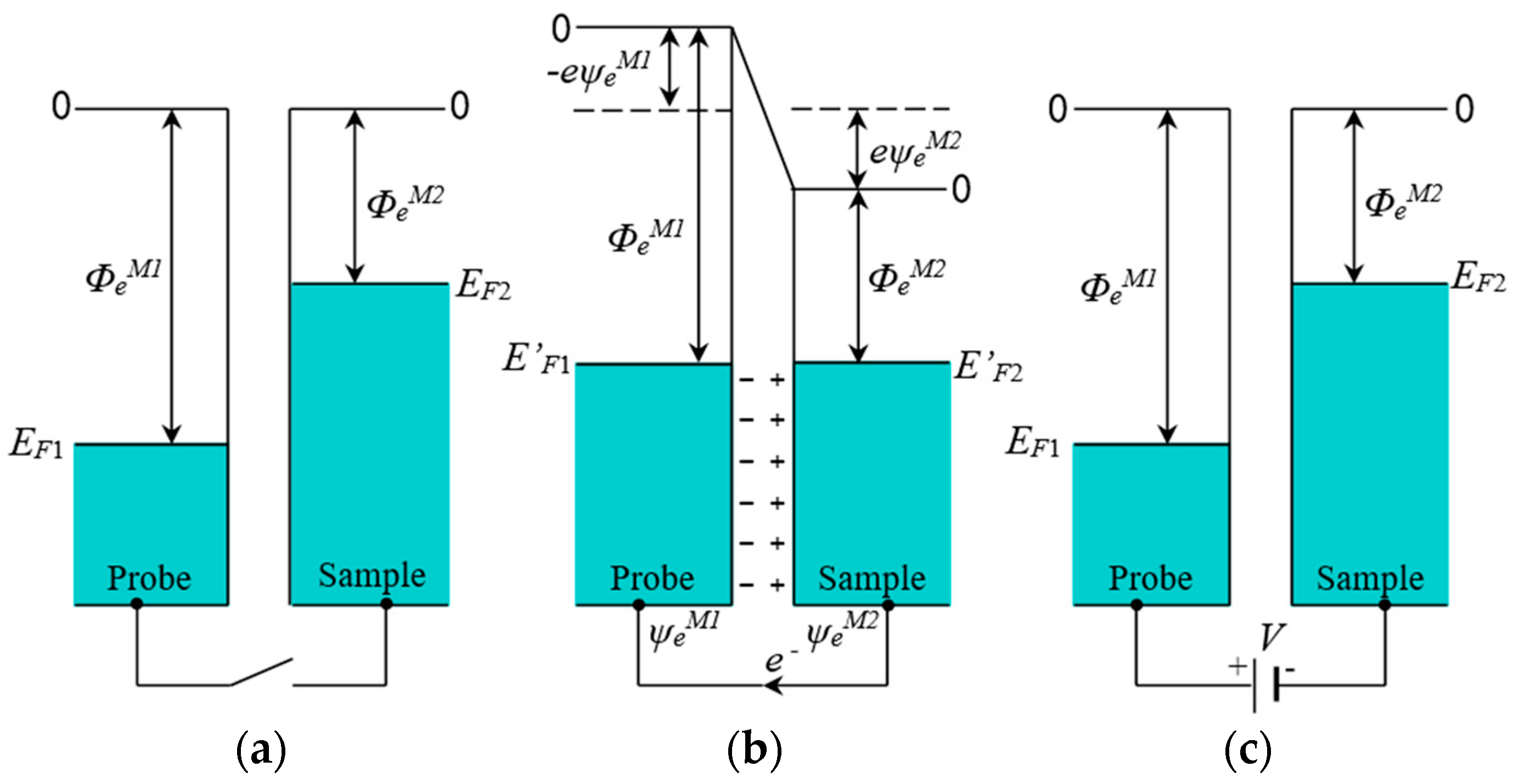
30]. According to the above analysis, a schematic diagram of the Scanning Kelvin Probe Microscope (SKPM) test was drawn and is shown in
Figure 7a.
In
Figure 7a,
and
are the Fermi energies of the probe and sample, respectively, and
and
are the electric work functions of the probe and the sample, respectively. Platinum was used as the probe material; its work function is higher than that of most of the metal materials, and its Fermi energy and electrochemical potential are lower [
31]. As shown in
Figure 7b, when the probe and sample were connected with a wire, the electron flowed from the sample to the probe because the electrochemical potential of the electron in the sample was higher until the electrochemical potentials and the Fermi energies of the sample and probe became equal and resulted in both the Fermi and vacuum levels of the sample and the probe moving without variation relative to the positions of one another [
28,
32]. Then the probe surface was negatively charged, and the Volta potential
(
) was generated; the sample surface was positively charged, and the Volta potential
(
) was also generated, so that a contact potential difference (
) was generated.
According to Formula (3),
The work function difference (
) between the sample and the probe is:
Formulas (5) and (8) were substituted into Formula (7) to deduce the relationship between the work function difference and the contact potential difference as Formula (9):
In the test mode, (
Figure 7c), an external voltage (
V) was applied using the instrument with the value equal to the opposite number of the contact potential difference (
) to make the surface charge of the probe and the sample equal to zero. The instrument recorded the value of the external voltage (
V) and then was used to calculate the work function difference between the sample and the probe [
23,
29,
30]. Therefore, the work function difference between the sample and the probe can be measured via the SKP method. The values obtained using the SKP method are always negative, and a more negative value indicates a lower work function of the sample.
From the definition of the work function, it becomes more difficult for the electron to escape from the surface of the tinplate when the surface is covered by a film and is in a passivated state after the passivation treatment. When the passivation film that covers the surface is thicker, it is more difficult for the electron to escape from the surface, and thus the work function is higher. In contrast, when the film is thinner, the work function is lower. Therefore, without considering other factors, it can be considered that when the work function difference measured via the SKP method is more negative, the passivation film is thinner, whereas when the work function is more positive, the passivation film is thicker.
3.3.2. Distribution State of the Work Function on the Tinplate Surface
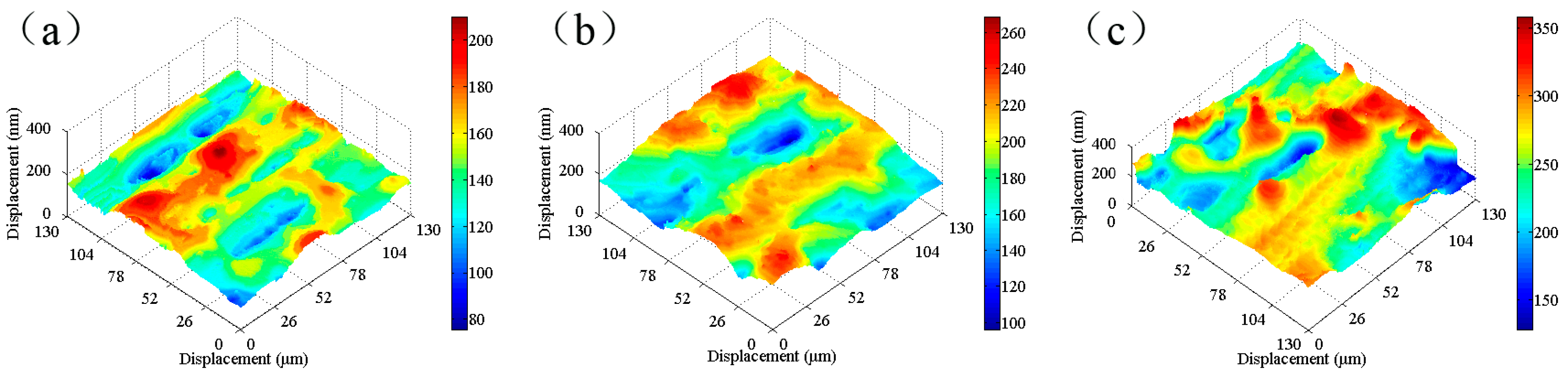
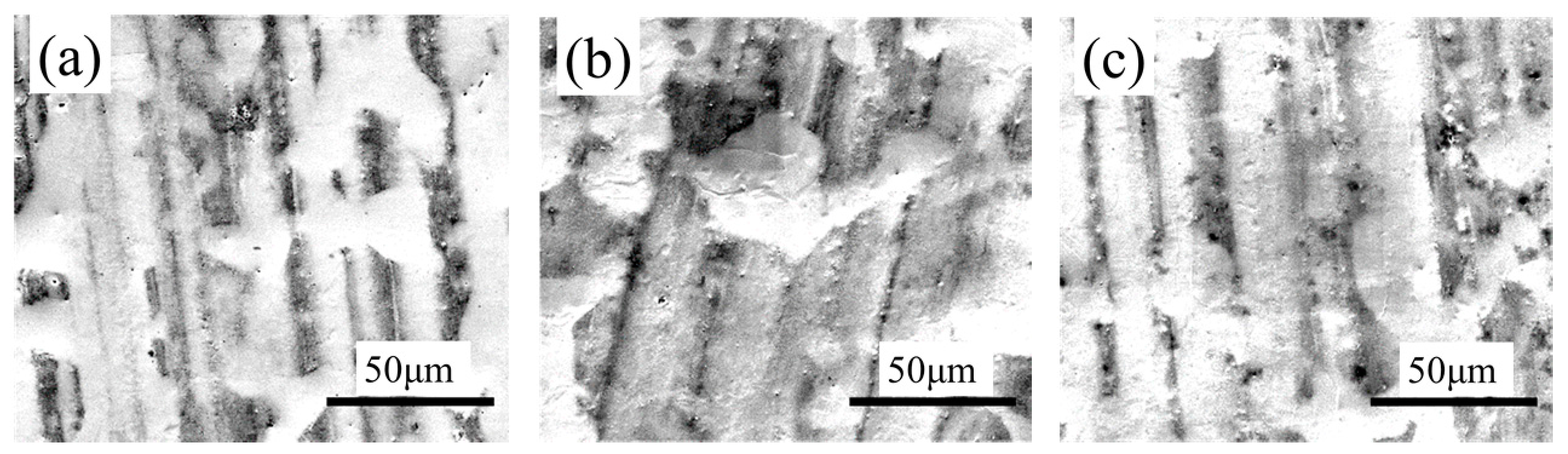
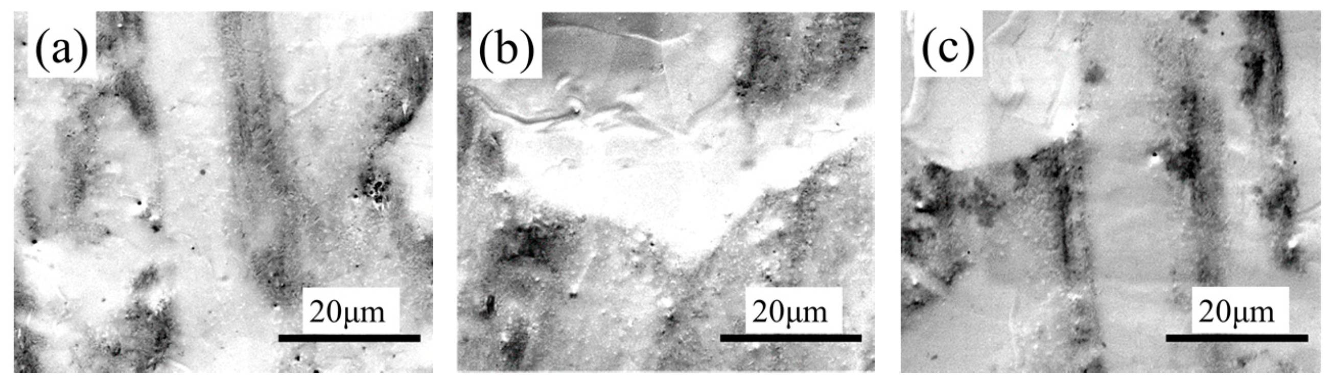
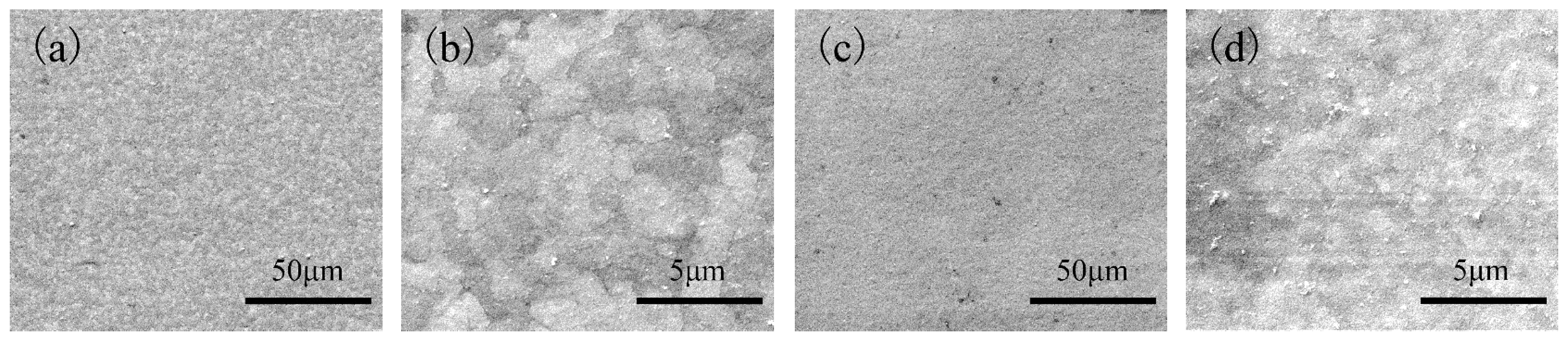
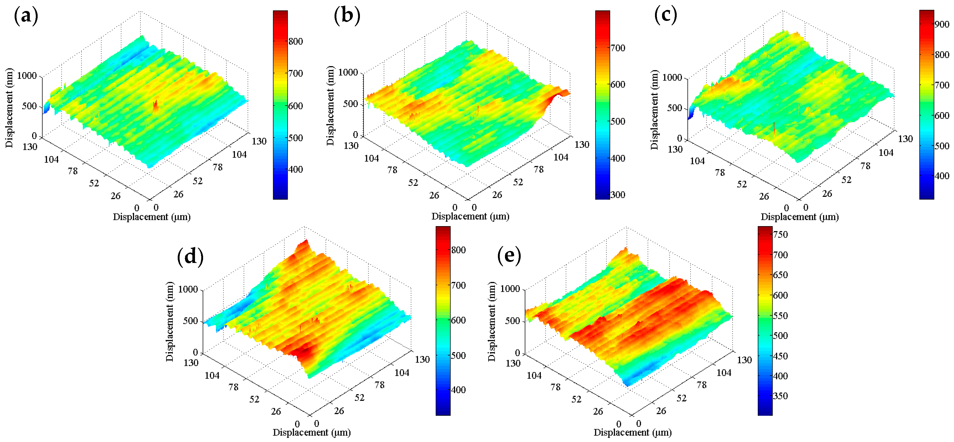
SKP tests were carried out on the tinplate samples before and after passivation using different treatment processes, and the results are shown in
Figure 8. The work function of the non-passivated tinplate (
Figure 8a) was mainly distributed between −0.65 and −0.55 eV. The uneven distribution of the work function on the surface of the tinplate indicates that the surface state was not uniform after reflowing. This may be because in the reflowing process in which the steel was heated via magnetic introduction, the distribution of the magnetic field on the steel surface was not absolutely uniform because it was affected by the surface evenness of the steel and the distribution state of the magnetic induction loop. There were differences in different areas on the surface of the steel in the degree of heat so that the oxides of tin were generated in different oxidation states in different areas of the surface. In addition, the steel surface state before reflowing may not be uniform. Thus, the states in different areas of the tinplate surface were not absolutely uniform, and hence the distribution of the work function was not uniform.
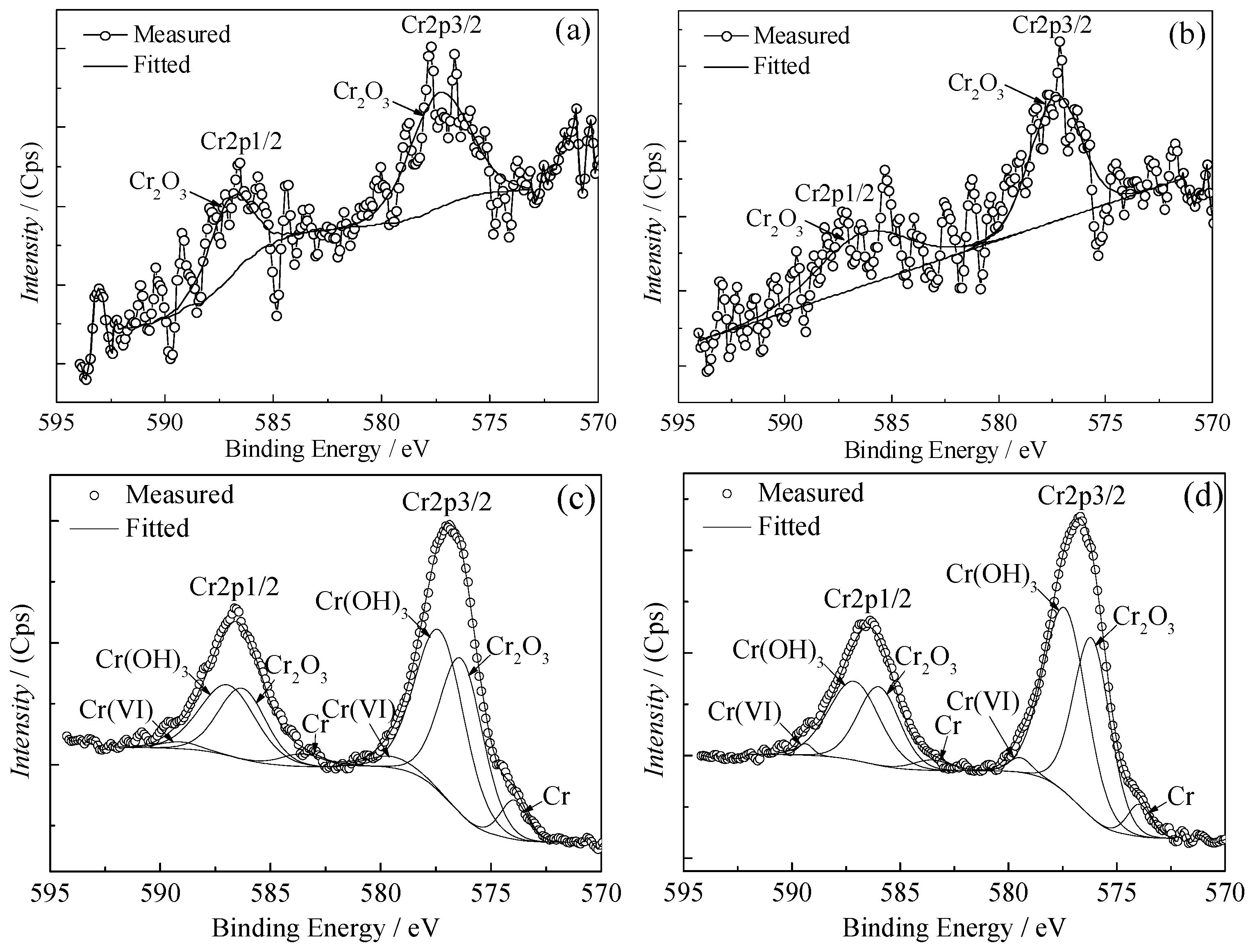
According to the passivation mechanism [
33], further oxidation of SnO
x (
) generated during the reflowing process and reduction of Cr(VI) occurred simultaneously in the chemical passivation process, and then the passivation film formed on the surface of the tinplate; this resulted in an increase in the work function. Further oxidation of SnO
x caused the oxidation state of tin in different areas on the tinplate surface to be uniform, and this resulted in a more uniform distribution of the work function on the surface.
Figure 8b shows that the work function of the tinplate after 3 s of chemical passivation was mainly distributed in the range of approximately −0.61 to −0.54 eV, and this generally increased slightly, although there was no obvious improvement in the distribution uniformity. Combined with the images shown in
Figure 6b, when the passivation process was conducted for a short time, the passivation film that formed on the tinplate surface was extremely thin, and there was a difference in the film thickness between that in the regions of microscopic bulges and that in the regions of valleys. Therefore, the work function did not significantly increase, and its distribution uniformity was not significantly improved. With longer passivation time, the work function of the tinplate after 6 s of chemical passivation was mainly distributed in the range of approximately −0.57 to −0.51 eV, as shown in
Figure 8c. In general, the work function further increased, and its distribution uniformity also improved obviously compared to that obtained with 3 s of passivation (
Figure 8b). With longer passivation time, more SnO
x was further oxidized, and the film thickness further increased, resulting in a further increase in the work function of the tinplate. A more uniform distribution of the film thickness (
Figure 6c) and the oxidation of more SnO
x led to a more uniform distribution of the work function.
Figure 8d shows that, after 3 s of electrolytic passivation, the work function of the tinplate was mainly distributed between −0.52 and −0.42 eV. In general, the work function increased significantly and was higher than that of the tinplate that had undergone chemical passivation, although its distribution uniformity degraded and had obvious high bulges and deep valleys. With longer passivation time, the work function of the tinplate was mainly distributed between −0.44 and −0.34 eV after electrolytic passivation for 6 s (
Figure 8e), and it further increased although its distribution uniformity further degraded and became worse. Because of the differences in the reaction mechanisms of electrolytic and chemical passivation (which are elaborated in the following section), the former passivation film was much thicker than the latter, although the former passivation film was distributed more unevenly on the tinplate surface than that of the latter (
Figure 6d,e).
It can be seen from the above results that the work function of the tinplate samples before and after passivation can be measured via SKP technology. The results indicate that the work function increased after both chemical and electrolytic passivation, and the latter increased more significantly than the former. The distribution of the work function on the tinplate surface became more uniform after chemical passivation, whereas it became worse after electrolytic passivation. For a certain amount of passivation time, the work function further increased with an increase in time for both the chemical and electrolytic methods; the distribution became more uniform when the chemical method was used, whereas it became worse when the electrolytic method was used. Thus, the distribution state of the nanoscale passivation film on the tinplate was deduced from the above geometrical topography images and the work function distribution maps.
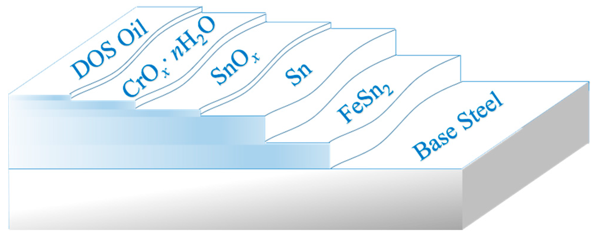
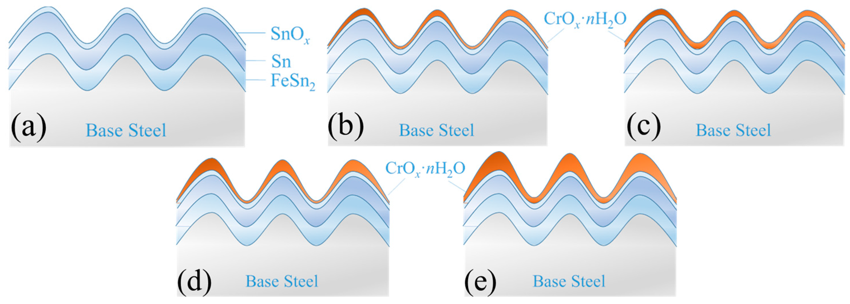
3.4. Distribution State of the Passivation Film on the Tinplate Surface
Before the distribution state of the passivation film on the surface of the tinplate is discussed, it is necessary to know the surface structure of the tinplate. It is generally believed that there is a five-layer structure forming the base steel of commercially available tinplate, and as shown in
Figure 9, the innermost layer is a tin-iron alloy (FeSn
2) layer [
34,
35]. The next layer is a metal tin layer for which there is no thermal diffusion reaction with the base iron during the reflowing process. The metal tin was oxidized simultaneously at a high temperature when reflowing, and then the tin oxide (SnO
x, (
)) layer formed on the metal tin [
36]. The passivation treatment was carried out after reflowing, and a chromic oxide film then formed on the tin oxide surface; the chemical composition of this film can be expressed as the general formula CrO
x·
nH
2O (mainly Cr
2O
3, Cr(OH)
3, with a small amount of Cr, Cr(VI)) [
8,
37,
38]. The outermost layer is an anti-rust oil film formed from electrostatic oil, which is usually dioctyl sebacate [
39,
40]. The thickness of the base steel is generally on the millimeter scale; the thickness of the alloy layer and the metal tin layer is on the micron scale; and the thicknesses of all three of the outer layers is on the nanoscale [
2,
12,
13].
The model shown in
Figure 9 is the ideal surface structure model of the tinplate, and the composition and structure of tinplate are clearly described. However, the surface of the tinplate may be more complicated. From the above surface roughness data of the tinplate, we know that the surface roughness cannot be neglected in the study of the interface structure of the tinplate.
Figure 10 shows a simplified structure model of the tinplate before and after passivated treatment with different processes. Aiming at illustrating the influence of surface roughness on the distribution state of the passivation film on the tinplate, in the model, we only consider the surface roughness instead of considering the surface defects of the tinplate, oil film, and other more complex surface conditions. According to geometrical topography images and SKP scanning maps, the surface structure model of the tinplate samples after passivation are depicted in
Figure 10b–e. The chemical passivation film was very thin and uniformly distributed on the tinplate surface. When the tinplate was passivated for a short time via the chemical method, the film that formed on the microscopic bulges was thicker than the film that formed in the microscopic valleys; however, the thickness difference was not very significant, as shown in
Figure 10b. When the tinplate was passivated for a longer time, the difference became very small, and so the film was distributed more uniformly on the tinplate surface, as shown in
Figure 10c. In general, the electrolytic passivation film was thicker than the chemical passivation film, but its distribution was uneven. When the tinplate was passivated for a short time via the electrolytic method, the film that formed on the microscopic bulges was thicker than that in the microscopic valleys, and the thickness difference was significant, as shown in
Figure 10d. When the tinplate was passivated for a longer time, the difference became greater, and the film was distributed more unevenly on the surface, as shown in
Figure 10e.
From a theoretical point of view, the reason why the topography and thickness of the chemical passivation and electrolytic passivation films are different is that the film formation mechanisms of the two methods are different. The former is a chemical reaction, whereas the latter is mainly an electrochemical reaction. In the chemical passivation process, SnOx () on the surface is needed to participate in the redox reaction. Thus, it can be imagined that the film attaches to the surface profile of the tinplate to form. In the initial stage of chemical passivation, the surface areas of the valleys do not make contact with the solution immediately, and it requires some time for the solution to reach the valleys. Thus, the reaction time between the microscopic bulges and valleys is different during the same passivation time. Therefore, when the passivation time was short, the areas in the valleys did not make sufficient contact with the solution to participate in the reaction, and thus the film in these areas was thinner. However, because the chemical passivation film was extremely thin in general, the differences in film thickness were not great. When the passivation time was long, the surface areas of the valleys made sufficient contact with the solution, and there was plenty of time to participate in the reaction. Thus, the film thickness further increased, and the result was that the difference between the film thicknesses of the valleys and that of the bulges decreased. Thus, the film was distributed more uniformly on the tinplate surface. Since SnOx is required in the chemical passivation process, after SnOx was oxidized and Cr(VI) was reduced to form the passivation film, it was difficult for the reaction on the passivation film to continue. As a result, it is difficult to further increase the thickness of the film. Therefore, the thickness of the passivation film is relatively thin.
In the electrolytic passivation process, although the chemical redox reactions occurred simultaneously, the process mainly relied on electrochemical action, specifically that Cr(VI) was reduced via cathodic electrolysis to form a Cr(III) oxides passivation film on the tinplate. This reduction reaction did not require the participation of SnOx and could even continue if the film had been covered; thus, the electrolytic passivation film was thicker than the chemical passivation film. However, the uneven thickness distribution of the electrolytic passivation film on the tinplate surface was mainly due to the nonuniform distribution of current density during galvanostatic electrolysis. The chrome electroplating process is characterized by a nonuniform thickness of the coating, and this is caused by the tip effect. In the electrolytic passivation process, the large surface roughness of the tinplate, which is used as the cathode, results in the tip effect occurring at microscopic bulges with high current density. In contrast, the current density at the microscopic valleys was low. For the same electrolysis time, the amount of current that passed through the bulges was high, whereas the amount of current that passed through the valleys was low. In addition, the long process of diffusion and mass transfer in the valleys cause the passivation reaction to be controlled by the diffusion of Cr(VI) ions. The hydrogen evolution reaction competes with the passivation reaction and results in a lower current efficiency. As a consequence, the film was thicker on the bulges but thinner in the valleys, and the difference in the film thickness caused the film distribution to be nonuniform.


