Article

Niobium-Containing DLC Coatings on Various Substrates for Strain Gauges

1
Institute for Surface Technology, Technical University Braunschweig, Bienroder Weg 54E, D-38108 Braunschweig, Germany
2
Institute of Microtechnology, Technical University Braunschweig, Alte Salzdahlumer Str. 203, D-38124 Braunschweig, Germany
3
Fraunhofer Institute for Surface Engineering and Thin Films (IST), Bienroder Weg 54E, D-38108 Braunschweig, Germany
*
Author to whom correspondence should be addressed.
Coatings 2019, 9(7), 417; https://doi.org/10.3390/coatings9070417
Submission received: 20 May 2019 / Revised: 14 June 2019 / Accepted: 26 June 2019 / Published: 29 June 2019

Abstract

:
Niobium-containing diamond-like carbon films (a-C:H:Nb) were deposited in a hybrid plasma-enhanced chemical vapor deposition (PECVD) and direct-current magnetron sputtering (DCMS) process, using a niobium target in an argon/acetylene atmosphere on industrial polyimide foil, spin-coated polyimide foil, and alumina substrates. While the coating on the industrial foil tends to crack, the thin films on the spin-coated polyimide and the ceramic substrates showed good adhesion, as well as a smooth and dense topography. Investigations of the electrical properties revealed their suitability as biocompatible sensor materials in strain gauges, with a gauge factor of up to 3.2 and a temperature coefficient of the electrical resistance (TCR) of −200 ppm/K.

1. Introduction

The deposition of thin films on flexible polymer foils is of growing interest, especially for microelectronic systems. Sensors or actuators on foils can be applied to complex work pieces; on places of poor accessibility; they can be removed and replaced easily and have good prospects for mass production by a roll-to-roll process. Also in the field of biomedical applications, sensor systems on polyimide have been successfully investigated for 25 years [1,2,3].
This investigation is concerned with the coating of a nanocomposite of niobium and carbon (a-C:H:Nb) on a polyimide foil as a base for biocompatible strain gauges with the objective of high sensitivity and low temperature dependence. A hybrid process of sputtering and PECVD was used, in which a niobium target was sputtered in an Ar + C2H2 atmosphere to produce an amorphous hydrogenated carbon layer (a-C:H) with enclosed NbxCy particles. This type of “metal-doped” material is often referred to as a-C:H:Me or Me-DLC in the literature. The addition of metal to DLC has several effects on the material properties: it reduces the internal stress due to a promotion of the graphite phase and disorder in the DLC matrix at low metal ratios [4,5], it can increase the electrical conductivity over 15 orders of magnitude [6], and for Ni and Pd, it was possible to develop piezoresistive materials of high strain sensitivity combined with a low TCR [7,8,9]. Our earlier investigations of a-C:H:Nb stated its great potential for strain sensors with a gauge factor of 35.5 and an TCR near zero [10].
To manufacture systems of thin films on plastic foils, various problems have to be overcome that arise when physical vapor deposited thin films, which may be brittle, hard, and strained, shall be deposited on a soft and flexible polymer foil. Those different mechanical properties of coating and substrate can lead to delamination, crack formation in the coating, or furling of the complete system. Furthermore, the foil needs to withstand process temperatures and vacuum conditions of the physical vapor deposition (PVD) process. Therefore, the substrate has a significance for the entire sensor system that should not be underestimated. The following investigation serves to estimate the feasibility and application range of the a-C:H:Nb coating on polyimide foils.
Due to the difference in mechanical properties of coating and substrate, the intrinsic stress of the system requires special attention. Nearly every vacuum-deposited film is in a status of stress. The thin film stress is composed of external mechanical stress, thermal stress, and intrinsic stress. External forces like tension, compression, local shearing stress, or thermally induced stresses depend on the final application of the system and are summed up in the external stress. Thermal stress develops during the deposition process and is the result of mismatch of the thermal expansion coefficients of the coating and the substrate material. The intrinsic stress is induced by crystallographic flaws like voids or interstitial atoms which are built into the coating during the deposition [11].
Delamination or buckling of the coating occur if the film stress exceeds the force of adhesion between coating and substrate. The adhesion force is dependent on the number and the kind of chemical bonds between coating and substrate. A high intrinsic adhesion can be obtained by a reduced number of high energy covalent bonds or a high number of low energy bonds. But even if covalent bonds are developed, a high interfacial stress can lead to a reduced adhesion. This kind of stress is a consequence of lattice misfits between coating and substrate material. This leads to a poor adhesion of carbon on glass substrates, for example. A further factor for the consideration of adhesion is the surface roughness of the substrate: on a rough surface, there is a higher number of possible adhesive bonds available due to the higher effective area and mechanically interlocking. However, contamination, surface defects, and passivation of bonds can be augmented on rough surfaces [12].
Several investigations of the interface of DLC and polyimide stated its good adhesion properties [13,14]. Presumably, a low-mismatch interface and high-energetic covalent bonds between the carbon of the polymer and the carbon of the coating are causal therefor.
Given the interface fracture toughness is high enough to prevent delamination, an increased film stress can lead to the formation of cracks in the coating. Those can propagate from the surface to the interface. With respect to electrical behavior, this will interfere with the transport of charge carriers, which will lead to an abrupt increase in the electrical resistivity. This factor can superimpose the geometric and physical effects that otherwise lead to an increase in the electrical resistance under strain in piezoresistive materials. Therefore, the possibility of crack formation must be considered in the following investigation.

2. Materials and Methods

a-C:H:Nb films were deposited by a combined PECVD/PVD process using a 3” Torus cathode with balanced magnetron from Kurt J. Lesker equipped with a Nb (99.95%) target in an Ar/C2H2-atmosphere on two different sputtering systems (Kurt J. Lesker Company, Jefferson Hills, PA, USA). The coatings on an Impact Coating IC300 sputtering system were prepared using an Advanced Energy PinnacleTM 1300–3000 Vdc charging a HIPIMS 2000/1000 BP MAGPULS operated (Magpuls GmbH, Sinzheim, Germany) in DC mode with a target-substrate-distance of 12 cm and static substrate. The working pressure was kept constant at 1 Pa by a constant Ar gas flow of 32 sccm and varying acetylene gas flow of 0–5 sccm. Furthermore a setup with a rotating substrate holder was investigated using a Balzers BAS 450 PM (Oerlikon Balzers, Balzers, ‎Liechtenstein) equipped with the same 3” cathode at a target-substrate-distance of 5.5 cm. Here an Advanced Energy PinnacleTM 10 × 10 kW charged a Melec SPIK 2000A-20 (Melec GmbH, Baden Baden, Germany) used in DC mode at constant current. The working pressure was kept constant at 1 Pa, using a butterfly valve with a constant Ar gas flow of 90 sccm and varying acetylene gas flow of 0–6 sccm. The system base pressure was below 5 × 10⁻³ Pa, the sputtering duration was 15 min.
The evaluated substrates were ceramic substrates (Al2O3, Kyocera Fineceramics GmbH, Esslingen am Neckar, Germany), polyimide foils of 30 µm thickness (DUPONTTM Kapton® HN, DuPont de Nemours, Neu Isenburg, Germany), and foils of 9 µm thickness fabricated by spin-on polyimide precursor (HD Microsystems PI 2611, HD MicroSystemsTM, Neu-Isenburg, Germany) adhered to a 4”-borofloat glass wafer with chromium bonding layer (according to [15]). Structuring of substrates, necessary for electrical characterization, was realized by adherent shadow masks, shown in Figure 1.
TCR measurements were conducted by measuring the total resistance of the pattern by four-point probe while the substrates cooled down from 110 to 40 °C. The gauge factor is determined by stretching the substrates to 0.025% of total length and measuring the resulting change in total resistance. Each sample is stretched cyclical 5 times. Both, TCR and gauge factor measurements were done with a Keithley 2400 measuring unit (Cleveland, OH, USA) with 0.012% basic measure accuracy. Calculation of TCR and gauge factor are described elsewhere [10]. Film thickness as well as surface topography and average roughness were determined by a profilometer (DektakXT Bruker, Billerica, MA, USA; 0.4 nm repeatability). The chemical composition was measured by electron probe microanalysis EPMA (Cameca SX 100, Gennevilliers, France) and is given in atomic percent with a accuracy of ±0.5 at %. Film microstructure was investigated using scanning electron microscopy SEM (Zeiss Gemini 1520, Oberkochen, Germany). Hardness and Young’s modulus were quantified by a nano-indentation tester, namely a Fisherscope H100VP XY-PROG unit (Helmut Fischer GmbH, Sindelfingen, Germany), using a Vickers indenter, with a constant load of 10 mN and 5 indentations per sample. The penetration depth was 0.2 µm at a film thickness of more than one micron on ceramic substrates, which is 20% indentation depth. To ensure measurement of ‘film-only’ properties the indentation depth should be less than 10% to avoid substrate influence, according to the rule of thumb. In the present case this is negligible, because the plastic deformation in soft films on hard substrates is contained within the film [16] and indentation depth and film thickness was kept in the same range for all samples. Measurement of Young’s modulus is more strongly affected by the substrate, especially with a large elastic mismatch between film and substrate [16], and will therefore not be considered. Nanoindentation measurements might hence not reflect true film properties, but film-substrate system properties of Nb-DLC on ceramics. Residual stress was calculated on glass substrates of 100 µm thickness based on the Stoney equation, with a film thickness of 1 µm.

3. Results and Discussion

Earlier investigations in a static process showed promising results for a-C:H:Nb as strain sensor material on industrial polyimide foil (Kapton HN) with gauge factors of up to 35.5 and the possibility to adapt the TCR to values between ±100 ppm/K for both HIPIMS and DCMS processes [10]. To analyze the substrate impact on the system and enhance the reproducibility, coating experiments were carried out on ceramic substrates and a polyimide foil of lower surface roughness and higher homogeneity (PI 2611), coated in a dynamic process with rotating substrate holder.

3.1. Electrical Properties and Morphology

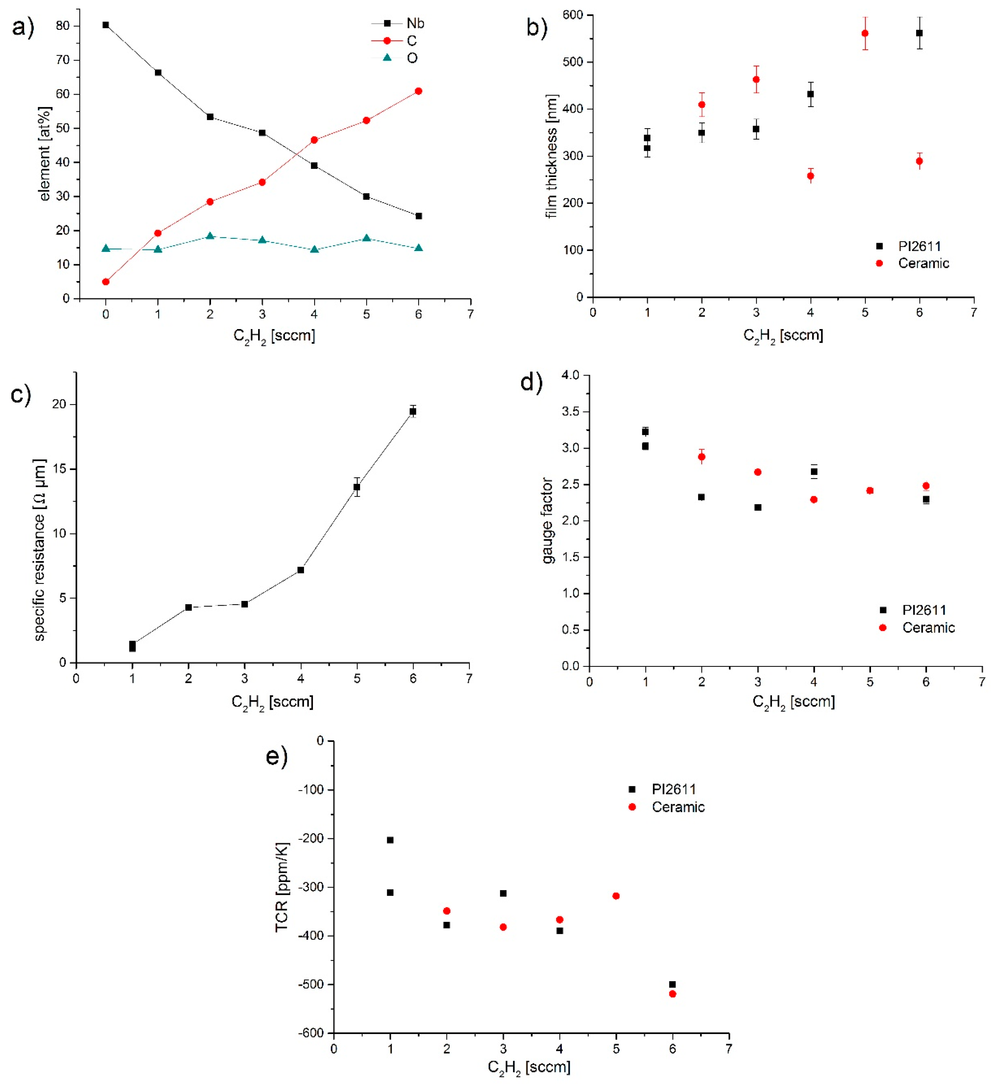
Results for the electrical properties and the chemical composition for the investigated processes are shown in Figure 2. Figure 2a shows that the chemical composition can be controlled by the C2H2 gas flow. A higher flow rate leads to an increase of the carbon fraction within the composite. This is not a linear relation, as the carbon is also poisoning the Nb target and thereby decreasing the sputter yield of the metal. The achieved Nb/C ratio on ceramics was found to be in the same range as previoulsy reported for a-C:H:Nb coatings on Kapton HN [10]. Along with the Nb/C ratio, the content of C–C bonds in the film is changed. Earlier investigations suggest that even at high Nb contents, there are still C–C bonds present, although Nb is a strong carbide former. It was proposed that films with low Nb content consist of small NbxCy nano-crystallites embedded in an amorphous a-C:H matrix, while higher Nb contents induce crystallite growth, until a phase transition at 50 at % results in segregation of cubic Nb with a NbxCy shell enclosed in the carbon matrix [10]. The sp2/sp3 ratio is a crucial parameter for the mechanical and electrical behavior of DLC coatings. Raman measurements for the a-C:H:Nb coatings were presented in [10]. There, an increase of the ID/IG ratio was observed for increasing metal content, which indicates an increase of the C sp2 content, and a higher disorder within the a-C:H:Nb. Also, a shift to higher wavenumbers for the D-peak location was detected, while the G-peak location stayed relatively constant at values between 1570 and 1589 cm−1. According to Robertson [17], this hints at a high C sp2 level corresponding to graphite or the nc-graphite phase and at a decrease in the disorder of the sp2 aromatic clusters.
The film thickness increased with the C2H2 gas flow, due to the higher amount of available deposition material. The specific resistance increased with the increasing precursor gas flow, as the NbxCy particles are shrinking in size when the metal content is decreasing in favor of an increasing carbon content. Therefore, the charge carriers will have to overcome wider distances in-between those conductive particles. In addition, the C sp2 fraction is diminished which causes an increase of electrical resistivity of the carbon matrix.
The gauge factor of the coatings on PI 2611 and ceramic reached its highest values (3.0–3.2) at the lowest C2H2 gas flows, but nevertheless, significantly below the previously measured values of more than 30 on Kapton HN. The TCR is slightly decreasing with increasing carbon content, as the a-C:H phase with its semiconducting behavior increases.
An overview of the electrical properties of a-C:H:Nb coatings on the different substrates is given in Table 1 for comparison. Although equal chemical compositions, thicknesses, and specific resistances could be generated on the newly investigated substrates (PI 2611, ceramics), the gauge factors of the new systems did not exceed values of 3.2.
The gauge factor is affected by geometrical and physical effects. As the geometry of the conductive path way was the same, geometric effects can be excluded as reason for the discrepancy in the electrical properties. To analyze the reasons for the large difference in gauge factor, a closer look on the coatings itself is necessary.
In Figure 3, the resistances of the strain sensor structures on Kapton HN and PI 2611 are shown as a function of time. The sensors are cyclically strained and relaxed. The coating on the Kapton HN foil shows a much higher piezoresistive effect with a gauge factor of 34.0 ± 0.9, but also a negative drift with a run-in behavior in the unstrained periods. The coating on the spin-coated polyimide foil has a lower piezoresistivity with a gauge factor of 2.3 ± 0.01 with nearly no drift in the resistance and an electrical resistance that is one order of magnitude lower.
In Figure 4, microscopic top-views of the coatings corresponding to the curves in Figure 2 are shown. The coating on the industrial foil shows a crack network that forms little clods. In addition, there are spots on the foil, which consist of enclosed blisters within the polyimide. Crack formation seems to originate primarily on these defect sites. The coating on the spin-coated polyimide foil on the other hand is homogeneous, and no cracks or defects can be seen. The crack formation can explain the high piezoresistive effect on the industrial foil. Under strain, the gaps between the cracks will widen and the resistance will increase severely. In addition, the run-in behavior in the relaxed phases could be caused by the cracks. As a-C:H:Nb coatings showing no cracks and a gauge factor of more than 5 could not be found, we have to state here, that the high piezoresistivity is obviously not caused by the formation of NbxCy particles in an amorphous carbon matrix like assumed in our first investigations [10], but instead can be attributed to crack formation.
In Figure 5, SEM images of the coatings on industrial polyimide foils are depicted. They reveal that the cracks commonly originate on the sites of defects. The pillar caps of the columnar grown coating mark the topography. The cracks seem to follow the column edges, where the cohesion forces of the coating are presumably the weakest.
In our earlier work we found, that elevated gauge factors on the industrial polyimide foil are only occurring at certain Nb contents of between 50 and 70 at %. This is also the region where the a-C:H:Nb growth turns from granular to more columnar morphology [10]. Columns are formed due to a low surface diffusion during sputtering [18]. Zhang et al. proposed an accumulation of the amorphous C-matrix in column boundaries, allowing them to glide [19]. Consequently, from the viewpoint of morphology, the region between columns is the weakest bond of a coating, indicating why the crack formation follows the column edges and occurs at these Nb contents. Figure 4 also shows that the crack formation occurs for both, HIPIMS and DCMS deposited coatings and is therefore not process dependent.

3.2. Stress and Hardness of a-C:H:Nb

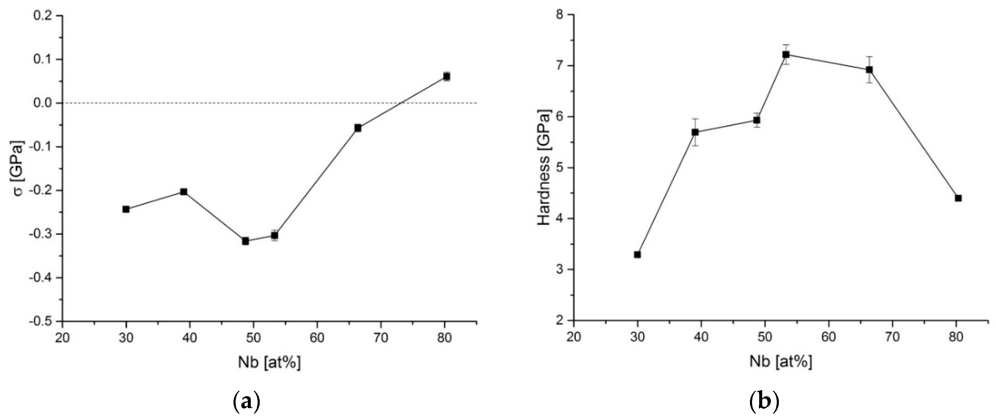
To better understand and avoid crack formation in order to enable a-C:H:Nb coatings on polyimide foils, an investigation of the major influence factors, especially the intrinsic stress was executed. Therefore, the residual stress as well as the hardness of a-C:H:Nb films in relation to the Nb content were measured as shown in Figure 6. When the Nb content is beneath 75 at % compressive stress occurs with its highest values at 48–53 at % Nb. At 80 at % Nb nearly metallic conditions of the coating lead to a slightly tensile residual stress of the coatings.
Other investigations at lower Nb-contents (Me/C-ratio up to 0.2) showed stress values around −2 GPa for pure DLC-films, decreasing to values as low as −0.02 GPa with Nb embedded in the DLC accompanied with a decreasing hardness [4,5]. Compared to these values the stress in the coatings of the present study is relatively low. Reason for the decrease of stress with increasing metal ratio is the decreasing content of C sp3 and relaxation of distorted bonds induced by the metal [4].
The small decrease in stress at 30 and 40 at % Nb could be due to a morphology change from columnar to granular with increasing C-ratio. At high C-content growing NbxCy crystallites are covered by the amorphous carbon phase during deposition [20], keeping the grain size of embedded particles low and leading to a granular morphology. The granular matrix is more flexible than the stiff columnar one.
The hardness of the coatings rises to its highest value of 7.2 ± 0.2 GPa with Nb content and then decreases abruptly when it turns into the primarily metallic phase. Reason for the strong increase of hardness in Figure 6 is the formation of hard niobium carbide particles, with the introduction of niobium. Zehnder et al. found for a-C:H:Ti, that the hardness is dependent on the grain size and grain separation distance, grains of below 10 nm radius and low separation distance of 0.5 nm lead to the highest values of hardness [21]. Presumably this is achieved for a-C:H:Nb with Nb contents of 50–70 at % in the used coating systems. On Kapton HN foils the elevated gauge factors as a result of crack formation were detected at Nb contents of 50–70 at %, which correlates with the increased film stress and the morphology change.

3.3. Thermally-Induced Intrinsic Stress

To estimate the influence of the thermally-induced intrinsic stress in the a-C:H:Nb/polyimide system and further validate the substrate influence, the thermal expansion coefficients (CTE) of coating and substrate need to be compared. In Table 2 the relevant coefficients are listed for the investigated substrates and also for DLC and NbC. There are no publications about the CTE of a-C:H:Nb known to the authors. As the investigated material is a nanocomposite of NbxCy particles in an a-C:H matrix the coefficients of a-C:H and NbxCy are used for rough estimations. Champi et al. investigated the thermal expansion of a-C:H coatings and found that an increase of the sp2 ratio leads to an increase in the CTE [22]. As the addition of Nb presumably induces a graphitization in the a-C:H, the matrix will tend to higher CTEs than a pure a-C:H coating. With increasing Nb content in the coating the NbxCy will play a dominant role for the CTE also. So we assume that the CTE of the investigated coatings will increase from values around 2 ppm/K to values around 6 ppm/K with increasing Nb content.
If this assumption is correct, the highest mismatch of CTEs is obtained in coatings on the industrial polyimide foil (Kapton HN) with a ΔCTE of 14 ppm/K for low Nb contents and 18 ppm/K for high Nb contents. For all other substrates, the mismatch is much lower. The crack formation occurred at high Nb contents between 50 and 70 at % Nb, so the thermal stress could be one of the major causes therefor. As the residual stress was determined on glass substrates, it cannot directly be compared to the thermal stress on Kapton HN.

3.4. Surface Roughness of the Substrates

In samples displaying cracks, the formation seems to be promoted by defects on the surface of the substrate (see Figure 4). To investigate if the surface roughness affects crack formation, it was determined for all used substrate materials before and after deposition. Sensor structures were deposited on all four substrate materials, under the same process conditions. The results are shown in Table 3. The Kapton HN foil exhibits a three times higher roughness than the spin-coated polyimide. Films on Kapton HN show six times higher value of roughness after deposition, while the roughness on the other substrates is only slightly increased. The high roughness on coated Kapton HN is caused by the crack formation. In the case of spin-coated polyimide the surface roughness was even diminished. While the coating on Kapton HN showed cracks and a high gauge factor, all other coatings were smooth and crack-free with a low gauge factor. Also the coating on the rough ceramic with an even higher surface roughness than Kapton HN did not show any cracks. From this we assume, that the crack formation is not caused by the surface roughness of the substrate itself, but the crack formation leads to an increased surface roughness after coating.
The investigation of substrate impact and reproducibility of high gauge factors on polyimide foils lead to the insight that crack formation caused the high piezoresistivity of sensor structures. Overall, the cracking could only be observed at certain Nb/C ratios and only on the industrial Kapton HN substrates. The main causes of crack formation are therefore the relatively high intrinsic stress in this layer composition in interrelation with the high CTE mismatch between Kapton HN and the coating. Furthermore, the columnar growth of these material compositions leads to defined breaking points of low cohesion force within the material. However, mainly the interplay of substrate and mechanical properties are causal for the cracks. By using spin-coated polyimide and polished ceramics, the problem of crack formation could be solved successfully and reproducibility of gauge factors up to 3 was established.

4. Conclusions

The presented investigations show that the harmonization of substrate and coating system is crucial for the overall system properties. It turned out that a-C:H:Nb tends to crack at distinct Nb/C ratios when coated on an industrial polyimide foil, while it forms defect-free and homogeneous films on a spin-coated polyimide of higher quality. Surface roughness (Ra) was varied in the range of 0.007 and 0.080 µm and could not be determined as cause for cracks, whereas the quality of the substrate surface is relevant as cracks originate from defects. Working points showing cracks at 1–2 sccm C2H2 flow, correlating with Nb contents of 50 to 70 at % are characterized by elevated compressive stress up to −0.3 ± 0.01 GPa probably due to high thermal stresses, because of the mismatch in expansion coefficient of film and substrate during deposition. The content of C sp3 bonds often specified in literature as the main reason for film stress, could not be held responsible for the high layer stress in the present case. High gauge factors of 35.5 for a-C:H:Nb on Kapton HN reported earlier [10] are obviously caused by crack formation, which is dependent on the substrate, and not a physical effect of the nanocomposite itself. Nevertheless, reliable results with reproducible piezoresistive behavior for thin films on polymeric materials were established on smooth polyimide PI 2611. For a-C:H:Nb on PI 2611 and on ceramic substrates, stable gauge factors of 2–3, with TCRs of −200 to −400 ppm/K and a good conductivity were achieved.

Author Contributions

Conceptualization, J.G., M.G., and R.B.; Validation, J.G. and M.G.; Formal Analysis, J.G. and M.G.; Investigation, M.G. and J.G.; Resources, G.B.; Writing—Original Draft Preparation, J.G. and M.G.; Writing—Review and Editing, R.B. and C.v.d.H.; Visualization, M.G.; Supervision, G.B. and A.D.; Project Administration, M.G.; Funding Acquisition, R.B., G.B., and A.D.

Funding

This work was funded by the German Research Foundation (DFG) (BR 2178/36-1). The APC was funded by Technical University Braunschweig.

Acknowledgments

The authors thank the Kurt J. Lesker Company for providing the sputtering source and target material.

Conflicts of Interest

The authors declare no conflict of interest.

References

  1. Lago, N.; Yoshida, K.; Koch, K.P.; Navarro, X. Assessment of biocompatibility of chronically implanted polyimide and platinum intrafascicular electrodes. IEEE Trans. Biomed. Eng. 2007, 54, 281–290. [Google Scholar] [CrossRef] [PubMed]
  2. Stieglitz, T.; Beutel, H.; Schuettler, M.; Meyer, J.-U. Micromachined, polyimide-based devices for flexible neural interfaces. Biomed. Microdevices 2000, 2, 283–294. [Google Scholar] [CrossRef]
  3. González, C.; Rodrı́guez, M. A flexible perforated microelectrode array probe for action potential recording in nerve and muscle tissues. J. Neurosci. Methods 1997, 72, 189–195. [Google Scholar] [CrossRef]
  4. Bouabibsa, I.; Lamri, S.; Sanchette, F. Structure, mechanical and tribological properties of Me-doped diamond-like carbon (DLC) (Me = Al, Ti, or Nb) hydrogenated amorphous carbon coatings. Coatings 2018, 8, 370. [Google Scholar] [CrossRef]
  5. Ding, J.C.; Dai, W.; Zhang, T.F.; Zhao, P.; Yun, J.M.; Kim, K.H.; Wang, Q.M. Microstructure and Properties of Nb-Doped Diamond-Like Carbon Films Deposited by High Power Impulse Magnetron Sputtering. Thin Solid Films 2018, 663, 159–167. [Google Scholar] [CrossRef]
  6. Köberle, H. Struktur und Elektrische LeitfäHigkeit von HF-Plasma-erzeugten Metallhaltigen Kohlenwasserstoffschichten. Ph.D. Thesis, University of Hamburg, Hamburg, Germany, 1989. [Google Scholar]
  7. Heckmann, U.; Bandorf, R.; Gerdes, H.; Lübke, M.; Schnabel, S.; Brauer, G. New materials for sputtered strain gauges. Procedia Chem. 2009, 1, 64–67. [Google Scholar] [CrossRef]
  8. Schultes, G.; Koppert, R.; Goettel, D.; Freitag-Weber, O.; Probst, A.C.; Werner, U. New perspectives for pressure and force sensors thin films combining high gauge factor and low TCR. In Smart Sensors, Actuators, and MEMS IV, Proceedings of SPIE Europe Microtechnologies for the New Millennium, Dresden, Germany, 4–6 May 2009; Schmid, U., Ed.; SPIE: Bellingham, WA, USA, 2009. [Google Scholar]
  9. Schultes, G.; Schmid-Engel, H.; Schwebke, S.; Werner, U. Granular metal–carbon nanocomposites as piezoresistive sensor films—Part 1: Experimental results and morphology. J. Sens. Sens. Syst. 2018, 7, 1–11. [Google Scholar] [CrossRef]
  10. Grein, M.; Bandorf, R.; Schiffmann, K.; Bräuer, G. Material structure and piezoresistive properties of niobium containing diamond-like-carbon films. Surf. Coat. Technol. 2019, 357, 273–279. [Google Scholar] [CrossRef]
  11. Thornton, J.A.; Hoffman, D. Stress-related effects in thin films. Thin Solid Films 1989, 171, 5–31. [Google Scholar] [CrossRef]
  12. Neuville, S.; Matthews, A. A perspective on the optimisation of hard carbon and related coatings for engineering applications. Thin Solid Films 2007, 515, 6619–6653. [Google Scholar] [CrossRef]
  13. Ordonez, J.S.; Boehler, C.; Schuettler, M.; Stieglitz, T. Long-term adhesion studies of polyimide to inorganic and metallic layers. MRS Proc. 2012, 1466. [Google Scholar] [CrossRef]
  14. Tai, F.-C.; Lee, S.-C.; Wei, C.-H. Spin-coating polyimide film on hydrogenated DLC film surface prepared by ion beam deposition method. Mater. Trans. 2006, 47, 1869–1873. [Google Scholar] [CrossRef]
  15. Von Der Heide, C.; Grein, M.; Dietzel, A. Femtosecond laser-contoured micro-strain gages. Microelectron. Eng. 2019, 214, 81–86. [Google Scholar] [CrossRef]
  16. Saha, R.; Nix, W.D. Effects of the substrate on the determination of thin film mechanical properties by nanoindentation. Acta Mater. 2002, 50, 23–38. [Google Scholar] [CrossRef]
  17. Robertson, J. Properties and prospects for non-crystalline carbons. J. Non-Cryst. Solids 2002, 299, 798–804. [Google Scholar] [CrossRef]
  18. Anders, A. A structure zone diagram including plasma-based deposition and ion etching. Thin Solid Films 2010, 518, 4087–4090. [Google Scholar] [CrossRef]
  19. Zhang, K.; Wen, M.; Cheng, G.; Li, X.; Meng, Q.; Lian, J.; Zheng, W. Reactive magnetron sputtering deposition and characterization of niobium carbide films. Vacuum 2014, 99, 233–241. [Google Scholar] [CrossRef]
  20. El Mel, A.A.; Bouts, N.; Grigore, E.; Gautron, E.; Granier, A.; Angleraud, B.; Tessier, P.-Y. Shape control of nickel nanostructures incorporated in amorphous carbon films: From globular nanoparticles toward aligned nanowires. J. Appl. Phys. 2012, 111, 114309. [Google Scholar] [CrossRef]
  21. Zehnder, T. Nanostructural and mechanical properties of nanocomposite nc-TiC/a-C:H films deposited by reactive unbalanced magnetron sputtering. J. Appl. Phys. 2004, 95, 4327. [Google Scholar] [CrossRef]
  22. Champi, A.; Lacerda, R.; Viana, G.; Marques, F. Thermal expansion dependence on the sp2 concentration of amorphous carbon and carbon nitride. J. Non-Cryst. Solids 2004, 338, 499–502. [Google Scholar] [CrossRef]
  23. Marques, F.C.; Lacerda, R.G.; Champi, A.; Stolojan, V.; Cox, D.C.; Silva, S.R.P. Thermal expansion coefficient of hydrogenated amorphous carbon. Appl. Phys. Lett. 2003, 83, 3099. [Google Scholar] [CrossRef]
  24. Wang, J.; Sugimura, Y.; Evans, A.; Tredway, W. The mechanical performance of DLC films on steel substrates. Thin Solid Films 1998, 325, 163–174. [Google Scholar] [CrossRef]
  25. Nelson, J.B.; Riley, D.P. The thermal expansion of graphite from 15 °C to 800 °C: Part I. Experimental. Proc. Phys. Soc. 1945, 57, 477–486. [Google Scholar] [CrossRef]
  26. Kempter, C.; Storms, E. Thermal expansion of some niobium carbides. J. Less Common Met. 1967, 13, 443–447. [Google Scholar] [CrossRef]
Figure 1. Schematic picture of the shadow mask used to generate the strain gauge structure.
Coatings 09 00417 g001
Figure 2. Chemical composition (a), film thickness (b), specific resistance (c), gauge factor (d) and TCR (e) of a-C:H:Nb coatings on polyimide substrates and ceramic substrates as function of the C2H2 flow rate. The specific resistance was determined on polyimide foil, the chemical composition on ceramic substrates. All processes where conducted in DCMS using a Balzers BAS 450 PM and deposition time of 15 min.
Coatings 09 00417 g002
Figure 3. Resistance measurement of a-C:H:Nb coatings mode under cyclic strain. The coating on the industrial polyimide foil (a) shows a high piezoresistivity with a gauge factor of 34 ± 0.9. The coating on the spin-coated polyimide foil (b) shows a much more stable behavior, but also a low piezoresistivity with a gauge factor of 2.3 ± 0.01. The cycle starts in strained conditions. The coatings were prepared in DCMS mode on IC300 (a) and BAS450 PM (b) with C2H2 flow of 2 sccm (a) and 1 sccm (b).
Coatings 09 00417 g003
Figure 4. Reflected light microscope images of the surface of the a-C:H:Nb coatings on the industrial foil (a) and the spin-coated polyimide foil (b). On the right picture the transition from coated (top) to un-coated (bottom) substrate is visible. The coating on the left side shows a crack network and a lot of defects within the foil. Depicted are the same samples as shown in Figure 2.
Coatings 09 00417 g004
Figure 5. SEM images showing the topography of the a-C:H:Nb coatings on the industrial polyimide foil. The left coating was prepared by DCMS (IC300, 1 sccm C2H2) with a gauge factor of 9.6 ± 0.2; the right coating was prepared by HIPIMS (IC300, 2 sccm C2H2) with a gauge factor of 10.9 ± 0.3. It is visible that the cracks are preferably starting on defects and are following the column edges.
Coatings 09 00417 g005
Figure 6. Residual stress (a) and hardness (b) of a-C:H:Nb films in relation to the Nb content at a constant working pressure of 1 Pa. The residual stress decreases with increasing Nb content, showing higher values around 50 at % Nb. The hardness increases with increasing Nb content and decreases when nearly metallic conditions are reached with 80 at % Nb.
Coatings 09 00417 g006
Table 1. Overview of the electrical properties of a-C:H:Nb coatings on different substrates. Given is the range between minimum and maximum values of comparable test series (DCMS mode, working pressure: 0.5 Pa, target power: 260 W) with acetylene gas flow variation.
SubstrateGauge FactorTCR (ppm/K)Specific Resistance (Ω µm)Sputter Unit
Industrial polyimide (Kapton HN)1.9–39.7−3900~+2501.5–1560IC300, BAS 450 PM
Spin-coated polyimide (PI 2611)2.2–3.2−500~−2003.3–34.6BAS 450 PM
Ceramic, Al2O3 polished2.3–2.9−520~−320BAS450 PM
Table 2. Thermal expansion coefficients of the used substrates and coating materials. For a-C:H:Nb no data could be found in literature. Instead data for a-C:H, graphite and NbxCy is displayed.
MaterialThermal Expansion Coefficient (ppm/K)ΔCTE between Substrate and Coating (ppm/K)References
Polyimide, Kapton HN2014–18Manufacturer specification
Polyimide, HD Microsystems PI 261131–3Manufacturer specification
Glass, borofloat3.251.25–2.75Manufacturer specification
Ceramic, Al2O37.21.2–5.2Manufacturer specification
Hard a-C:H1.5–7[23,24]
Graphite, Perpendicular to the basal plane27−1.5[25]
Graphite, Parallel to the basal plane Average8
NbxCy5.89–6.23[26]
a-C:H:Nb2–6assumption of this work
Table 3. Roughness of uncoated and coated substrates, gauge factors and TCRs of corresponding films.
SubstrateRa before Coating (µm)Ra after Coating (µm)Gauge FactorTCR (ppm/K)
Industrial polyimide (Kapton HN)0.065 ± 0.0280.420 ± 0.15010.2 ± 0.45+110
Spin-coated polyimide (PI 2611)0.023 ± 0.0130.007 ± 0.0043.22 ± 0.06−203
Ceramic, Al2O3, polished0.007 ± 0.0020.030 ± 0.0172.68 ± 0.01−203
Ceramic, Al2O3, rough0.080 ± 0.0350.140 ± 0.0302.48 ± 0.04−413