Growth of GaN Thin Film on Amorphous Glass Substrate by Direct-Current Pulse Sputtering Deposition Technique


Abstract
1. Introduction
2. Materials and Methods
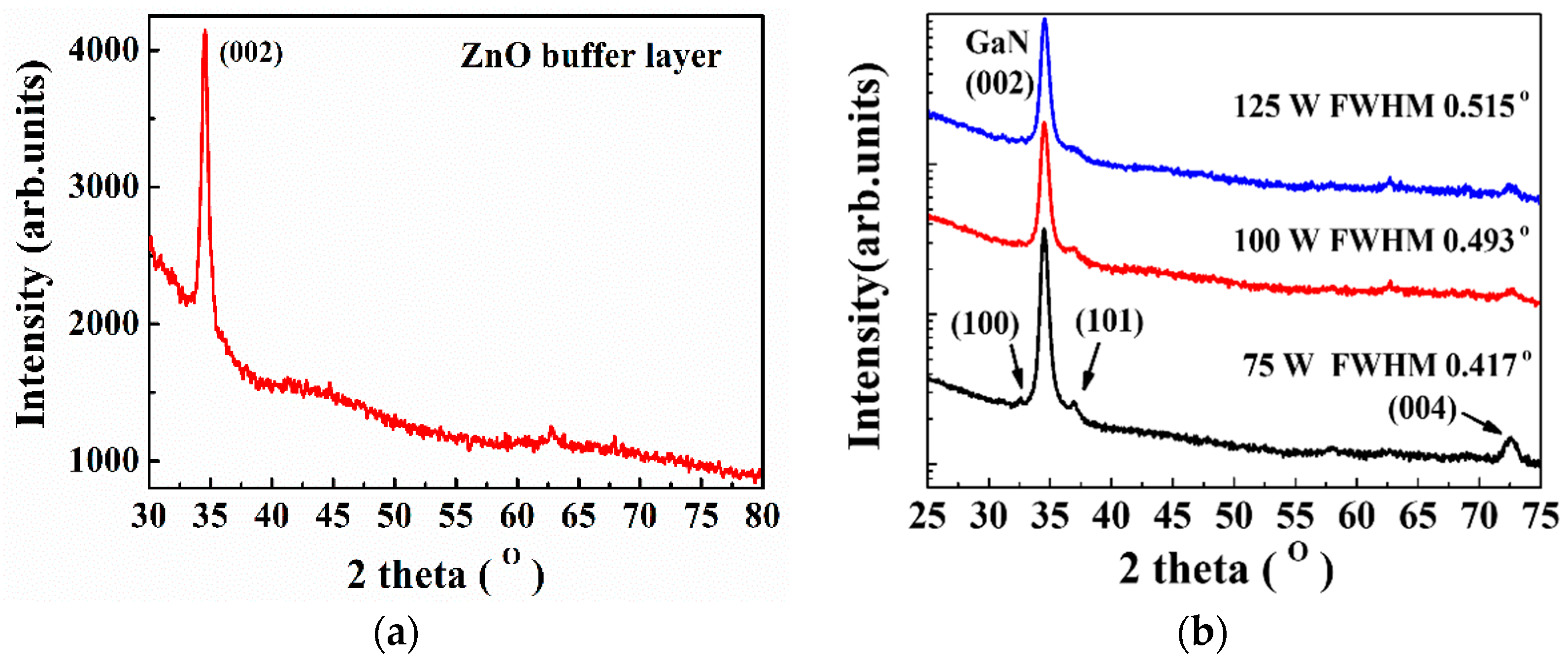
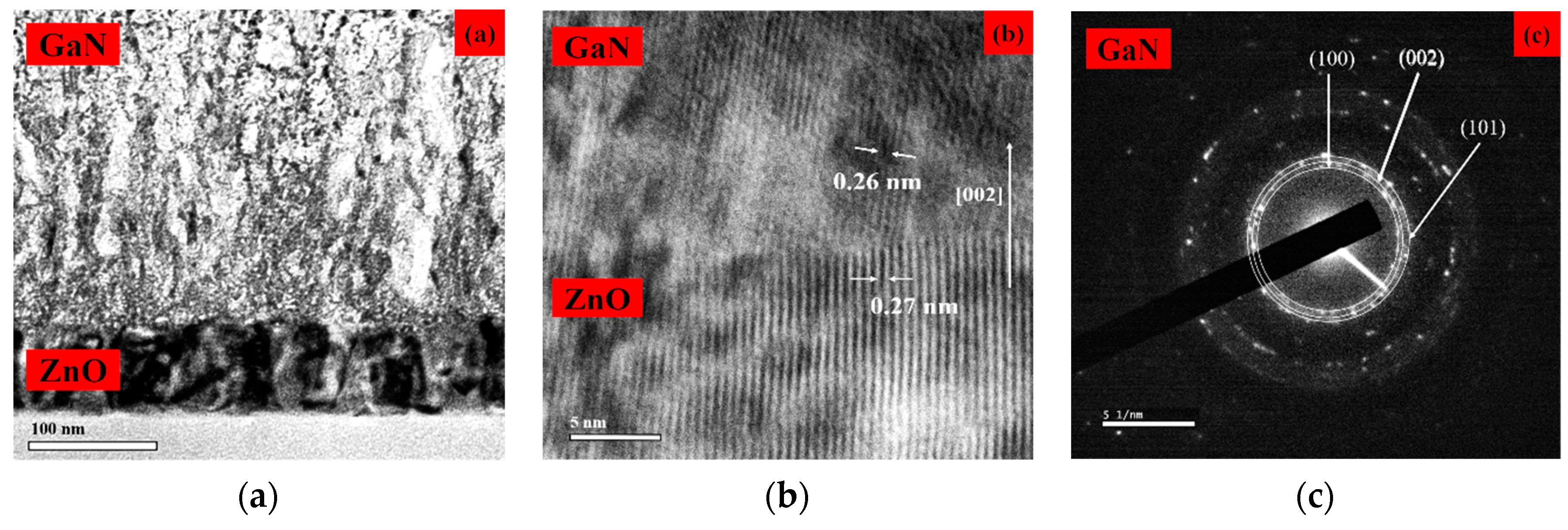
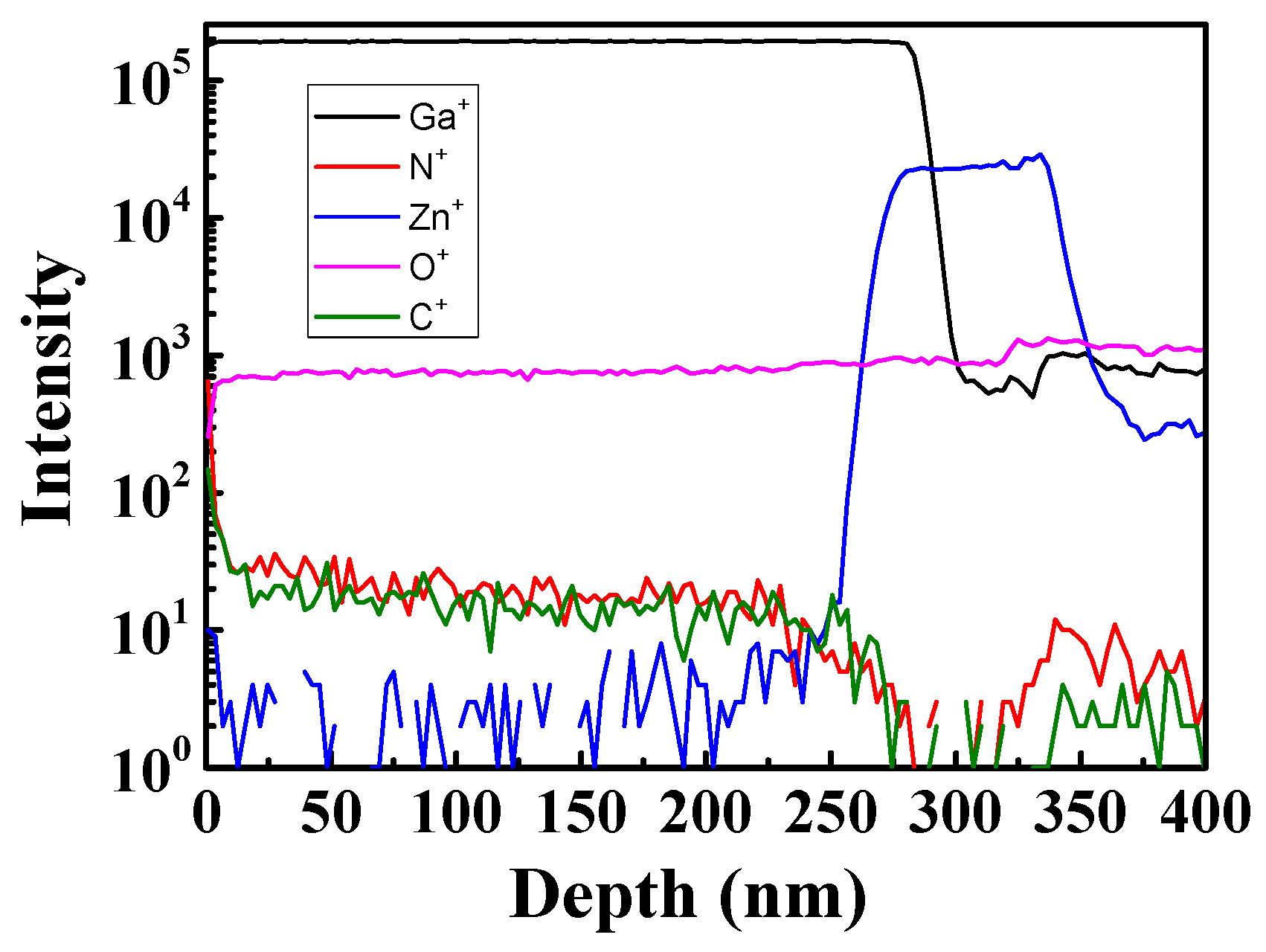
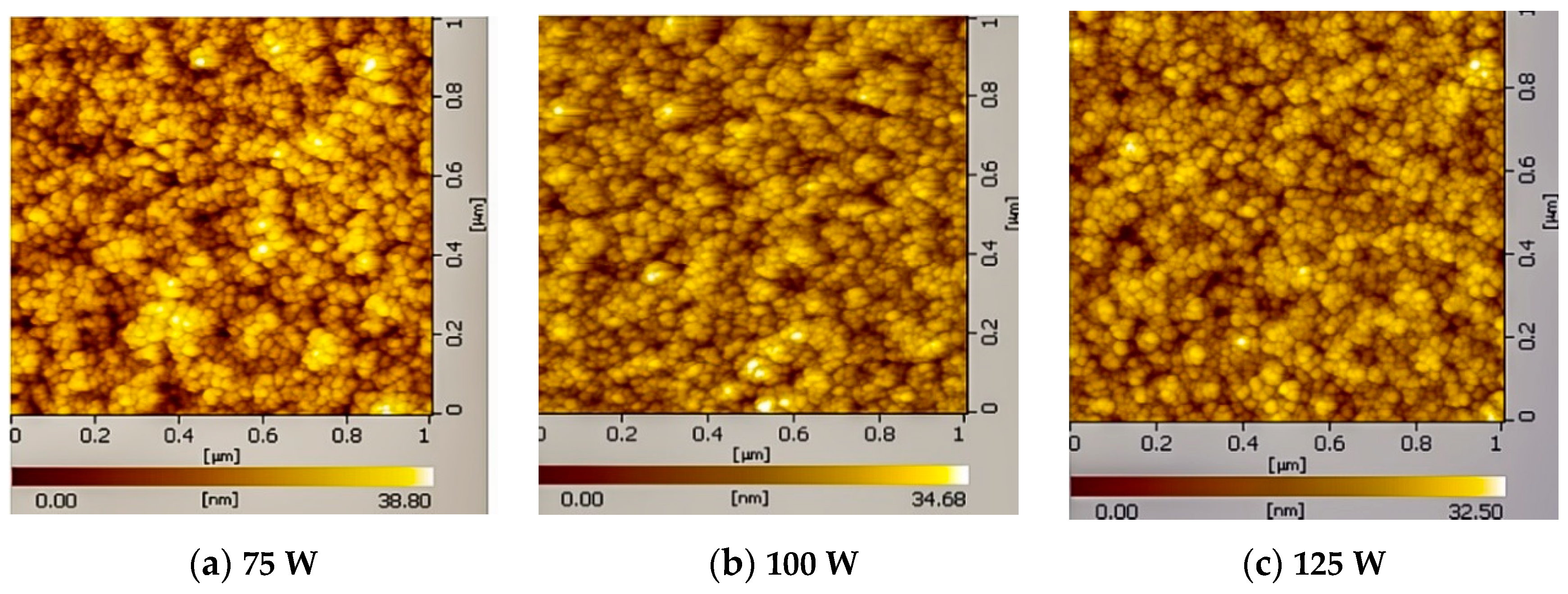
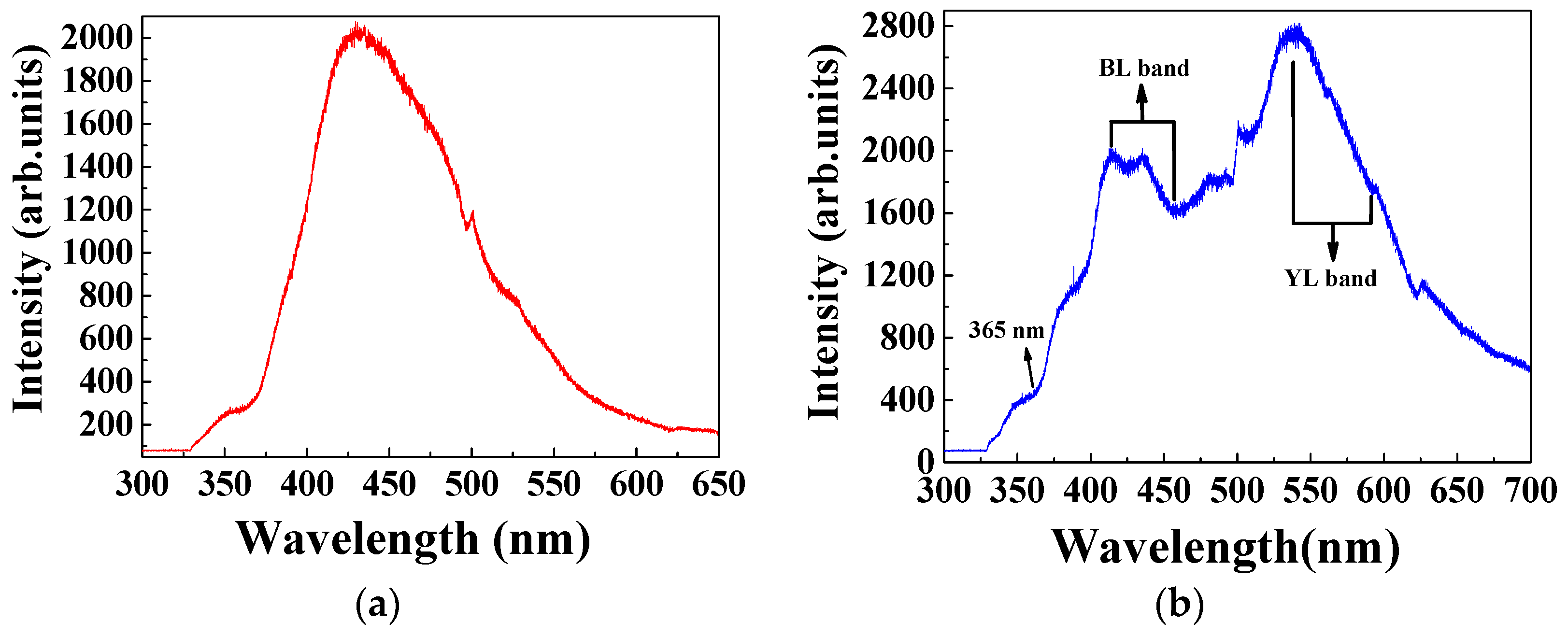
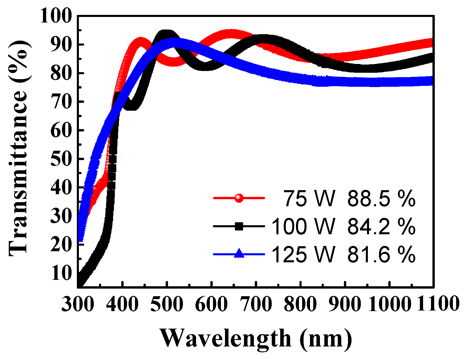
3. Results and Discussions
4. Conclusions
Author Contributions
Funding
Acknowledgments
Conflicts of Interest
References
- Jain, S.C.; Willander, M.; Narayan, J.; van Overstraeten, R. III–nitrides: Growth, characterization, and properties. J. Appl. Phys. 2000, 87, 965–1006. [Google Scholar] [CrossRef]
- Kumakura, K.; Makimoto, T. Carrier transport mechanisms of Pnp AlGaN/GaN heterojunction bipolar transistors. Appl. Phys. Lett. 2008, 92, 093504. [Google Scholar] [CrossRef]
- Wang, X.L.; Wang, C.M.; Hu, G.X.; Wang, J.X.; Chen, T.S.; Jiao, G.; Li, J.P.; Zeng, Y.P.; Li, J.M. Improved DC and RF performance of AlGaN/GaN HEMTs grown by MOCVD on sapphire substrates. Solid-State Electron 2005, 49, 1387–1390. [Google Scholar] [CrossRef]
- Liu, L.; Edgar, J.H. Substrates for gallium nitride epitaxy. Mater. Sci. Eng. R 2002, 37, 61–127. [Google Scholar] [CrossRef]
- Tokunaga, H.; Tan, H.; Inaishi, Y.; Arai, T.; Yamaguchi, A.; Hidaka, J. Performance of multiwafer reactor GaN MOCVD system. J. Crystal Growth 2000, 221, 616–621. [Google Scholar] [CrossRef]
- Hughes, W.C.; Rowland, W.H., Jr.; Johnson, M.A.L.; Fujita, S.; Cook, J.W., Jr.; Schetzina, J.F. Molecular beam epitaxy growth and properties of GaN films on GaN/SiC substrates. J. Vac. Sci. Technol. B 1995, 13, 1571–1577. [Google Scholar] [CrossRef]
- Yu, H.; Chen, L.; Zhang, R.; Xiu, X.; Xie, Z.; Ye, Y.; Gu, S.; Shen, B.; Shi, Y.; Zheng, Y. The growth of GaN films on Si substrates by HVPE. Mater. Sci. Forum 2005, 475–479, 3783–3786. [Google Scholar] [CrossRef]
- Grandjean, N.; Massies, J.; Martinez, Y.; Vennegues, P.; Leroux, M.; Laugt, M. GaN epitaxial growth on sapphire (0 0 0 1): the role of the substrate nitridation. J. Crystal Growth 1997, 178, 220–228. [Google Scholar] [CrossRef]
- Zou, C.W.; Wang, H.J.; Yin, M.L.; Li, M.; Liu, C.S.; Guo, L.P.; Fu, D.J.; Kang, T.W. Preparation of GaN films on glass substrates by middle frequency magnetron sputtering. J. Crystal Growth 2009, 311, 223–227. [Google Scholar] [CrossRef]
- Zou, C.W.; Yin, M.L.; Li, M.; Liu, C.S.; Guo, L.P.; Fu, D.J. GaN films deposited on glass substrate by middle-frequency magnetron sputtering. Thin Solid Films 2008, 517, 670–673. [Google Scholar] [CrossRef]
- Sato, Y.; Kurosaki, A.; Sato, S. Low-temperature growth of GaN and InxGa1~xN films on glass substrates. J. Crystal Growth 1998, 189/190, 42–46. [Google Scholar] [CrossRef]
- Sellers, J. Asymmetric bipolar pulsed DC: the enabling technology for reactive PVD. Surf. Coat. Technol. 1998, 98, 1245–1250. [Google Scholar] [CrossRef]
- Kelly, P.J.; Arnell, R.D. Magnetron sputtering: A review of recent developments and applications. Vacuum 2000, 56, 159–172. [Google Scholar] [CrossRef]
- Schiller, S.; Goedicke, K.; Reschke, J.; Kirchhoff, V.; Schneider, S.; Milde, F. Pulsed magnetron sputter technology. Surf. Coat. Technol. 1993, 61, 331–337. [Google Scholar] [CrossRef]
- Barshilia, H.C.; Rajam, K.S. Reactive sputtering of hard nitride coatings using asymmetric-bipolar pulsed DC generator. Surf. Coat. Technol. 2006, 201, 1827–1835. [Google Scholar] [CrossRef]
- Hultman, L.; Helmersson, U.; Barnett, S.A.; Sundgren, J.E.; Greene, J.E. Low-energy ion irradiation during film growth for reducing defect densities in epitaxial TiN (100) films deposited by reactive-magnetron sputtering. J. Appl. Phys. 1987, 61, 552–555. [Google Scholar] [CrossRef]
- Jonsson, L.B.; Nyberg, T.; Katardjiev, I.; Berg, S. Frequency response in plused DC reactive sputtering processes. Thin Solid Films 2000, 365, 43–48. [Google Scholar] [CrossRef]
- Sun, X.W.; Xiao, R.F.; Kwok, H.S. Epitaxial growth of GaN thin film on sapphire with a thin ZnO buffer layer by liquid target pulsed laser deposition. J. Appl. Phys. 1998, 84, 5776–5779. [Google Scholar] [CrossRef]
- Xue, S.; Zhang, X.; Huang, R.; Zhuang, H. Effects of the sputtering time of ZnO buffer layer on the quality of GaN thin films. Appl. Surf. Sci. 2008, 254, 6766–6769. [Google Scholar] [CrossRef]
- Zou, C.W.; Zhanga, J.; Xie, W.; Shao, L.X.; Guo, L.P.; Fu, D.J. Characterization and properties of GaN films deposited by middle-frequency magnetron sputtering with anode-layer ion source assistance. Vacuum 2011, 86, 280–284. [Google Scholar] [CrossRef]
- Shi, F. GaN Nanowires Fabricated by Magnetron Sputtering Deposition. In Nanowires—Fundamental Research; Hashim, A.A., Ed.; InTech: London, UK, 2011; p. 265-262. ISBN 978-953-307-327-9. [Google Scholar]
- Martínez-Ara, L.A.; Aguilar-Hernández, J.R.; Sastré-Hernández, J.; Hernández-Hernández, L.A.; Hernández-Pérez, M.d.; Maldonado-Altamirano, P.; Mendoza-Pérez, R.; Contreras-Puente, G. Structural and optical properties of GaN thin films grown on Si (111) by pulsed laser deposition. Mater. Res. 2019, 22, e20180263. [Google Scholar] [CrossRef]
- Zhang, J.Z.L.D.; Wang, X.F.; Liang, C.H.; Peng, X.S.; Wang, Y.W. Fabrication and photoluminescence of ordered GaN nanowire arrays. J. Chem. Phys. 2001, 115, 5714–5717. [Google Scholar] [CrossRef]
- Kim, K.H.; Park, K.C.; Ma, D.Y. Structural, electrical and optical properties of aluminum doped zinc oxide films prepared by radio frequency magnetron sputtering. J. Appl. Phys. 1997, 81, 7764–7772. [Google Scholar] [CrossRef]
- Liu, W.-S.; Wu, S.-Y.; Tseng, C.-H.; Hung, C.-Y. Development of high-quality titanium-doped gallium ZnO transparent conductive films by RF magnetron sputtering techniques. Phys. Status Solidi C 2013, 10, 1569–1572. [Google Scholar] [CrossRef]
- Liao, H.; Wei, T.; Zong, H.; Jiang, S.; Li, J.; Yang, Y.; Yu, G.; Wen, P.; lang, R.; Wang, W.; et al. Raman investigation on the surface carrier concentration of single GaN microrod grown by MOCVD. Appl. Surf. Sci. 2019, 489, 346–350. [Google Scholar] [CrossRef]
- Kouvetakis, J.; Beach, D.B. Chemical vapor deposition of gallium nitride from diethylgallium azide. Chem. Mater. 1989, 1, 476–478. [Google Scholar] [CrossRef]
- Bagavath, C.; Nasi, L.; Kumar, J. Investigations on the nanostructures of GaN, InN and InxGa1−xN. Mater. Sci. Semicond. Process. 2016, 49, 61–67. [Google Scholar] [CrossRef]
- Ozgit-Akgun, C.; Kayaci, F.; Vempati, S.; Haider, A.; Celebioglu, A.; Goldenberg, E.; Kizir, S.; Uyar, T.; Biyikli, N. Fabrication of flexible polymer-GaN core-shell nanofibers by the combination of electrospinning and hollow cathode plasma-assisted atomic layer deposition. J. Mater. Chem. C 2015, 3, 5199–5206. [Google Scholar] [CrossRef]
- Duygulu, N.E.; Kodolbas, A.O.; Ekerim, A. Effects of argon pressure and r.f. power on magnetron sputtered aluminum doped ZnO thin films. J. Crystal Growth 2014, 394, 116–125. [Google Scholar] [CrossRef]
- Saad, M.; Kassis, A. Effect of rf power on the properties of rf magnetron sputtered ZnO: Al thin films. Mater. Chem. Phys. 2012, 136, 205–209. [Google Scholar] [CrossRef]
- Jacob, D.; Chitra, M. Formation of GaN thin film on silicon substrate by gallium oxide Ammoniation. Optik 2018, 171, 51–57. [Google Scholar]
- As, D.J.; Schmilgus, F.; Wang, C.; ttker, B.S.; Schikora, D.; Lischka, K. The near band edge photoluminescence of cubic GaN epilayers. Appl. Phys. Lett. 1997, 70, 1311–1313. [Google Scholar] [CrossRef]
- Schuberta, E.F.; Goepfert, I.D.; Grieshaberb, W. Optical properties of Si-doped GaN. Appl. Phys. Lett. 1997, 71, 921–923. [Google Scholar] [CrossRef][Green Version]
- Reshchikov, M.A.; Morkoç, H. Luminescence properties of defects in GaN. J. Appl. Phys. 2005, 97, 061301. [Google Scholar] [CrossRef]
- Reshchikov, M.A.; Shahedipour, F.; Korotkov, R.Y.; Ulmer, M.P.; Wessels, B.W. Deep acceptors in undoped GaN. Phys. B 1999, 273–274, 105–108. [Google Scholar] [CrossRef]
- Reshchikov, M.A.; Shahedipour, F.; Korotkov, R.Y.; Wessels, B.W.; Ulmer, M.P. Photoluminescence band near 2.9 eV in undoped GaN epitaxial layers. J. Appl. Phys. 2000, 87, 3351–3354. [Google Scholar] [CrossRef]
- Xue, S.; Zhang, X.; Huang, R.; Zhuang, H. Surface morphology of ZnO buffer layer and its effects on the growth of GaN films on Si substrates by magnetron sputtering. Appl. Phys. A 2009, 94, 287–291. [Google Scholar] [CrossRef]
- Seager, C.H.; Wright, A.F.; Yu, J.; Gotz, W. Role of carbon in GaN. J. Appl. Phys. 2002, 92, 6553–6560. [Google Scholar] [CrossRef]
- Seager, C.H.; Tallant, D.R.; Yub, J.; Gotz, W. Luminescence in GaN co-doped with carbon and silicon. J. Luminesc. 2004, 106, 115–124. [Google Scholar] [CrossRef]
- Zhao, D.G.; Jiang, D.S.; Yang, H.; Zhu, J.J.; Liu, Z.S.; Zhang, S.M.; Liang, J.W.; Li, X.; Li, X.Y.; Gong, H.M. Role of edge dislocations in enhancing the yellow luminescence of n-type GaN. Appl. Phys. Lett. 2006, 88, 241917. [Google Scholar] [CrossRef]
- Neugebauer, J.; van de Walle, C.G. Gallium vacancies and the yellow luminescence in GaN. Appl. Phys. Lett. 1996, 69, 503–505. [Google Scholar] [CrossRef]
- Julkarnain, M.; Kamata, N.; Fukuda, T.; Arakawa, Y. Yellow luminescence band in undoped GaN revealed by two-wavelength excited photoluminescence. Opt. Mater. 2016, 60, 481–486. [Google Scholar] [CrossRef]
- Ito, S.; Nakagita, T.; Sawaki, N.; Ahn, H.S.; Irie, M.; Hikosaka, T.; Honda, Y.; Yamaguchi, M.; Amano, H. Nature of yellow luminescence band in GaN grown on Si substrate. Jpn. J. Appl. Phys. 2014, 53, 11RC02. [Google Scholar] [CrossRef]
- Reshchikov, M.A.; Demchenko, D.O.; Usikov, A.; Helava, H.; Makarov, Y. Carbon defects as sources of the green and yellow luminescence bands in undoped GaN. Phys. Rev. B 2014, 90, 235203. [Google Scholar] [CrossRef]
- Christenson, S.G.; Xie, W.; Sun, Y.Y.; Zhang, S.B. Carbon as a source for yellow luminescence in GaN: Isolated CN defect or its complexes. J. Appl. Phys. 2015, 118, 135708. [Google Scholar] [CrossRef]
- Yim, K.; Lee, C. Dependence of the electrical and optical properties of sputter-deposited ZnO: Ga films on the annealing temperature, time, and atmosphere. J Mater. Sci.: Mater. Electron. 2007, 18, 385–390. [Google Scholar]
- Liu, W.-S.; Wu, S.-Y.; Hung, C.-Y.; Tseng, C.-H.; Chang, Y.-L. Improving the optoelectronic properties of gallium ZnO transparent conductive thin films through titanium doping. J. Alloys Compd. 2014, 616, 268–274. [Google Scholar] [CrossRef]
- EKnox-Davies, C.; Shannon, J.M.; Silva, S.R.P. The properties and deposition process of GaN films grown by reactive sputtering at low temperatures. J. Appl. Phys. 2006, 99, 073503. [Google Scholar] [CrossRef]


© 2019 by the authors. Licensee MDPI, Basel, Switzerland. This article is an open access article distributed under the terms and conditions of the Creative Commons Attribution (CC BY) license (http://creativecommons.org/licenses/by/4.0/).
Share and Cite
Liu, W.-S.; Chang, Y.-L.; Chen, H.-Y. Growth of GaN Thin Film on Amorphous Glass Substrate by Direct-Current Pulse Sputtering Deposition Technique. Coatings 2019, 9, 419. https://doi.org/10.3390/coatings9070419
Liu W-S, Chang Y-L, Chen H-Y. Growth of GaN Thin Film on Amorphous Glass Substrate by Direct-Current Pulse Sputtering Deposition Technique. Coatings. 2019; 9(7):419. https://doi.org/10.3390/coatings9070419
Chicago/Turabian StyleLiu, Wei-Sheng, Yu-Lin Chang, and Hui-Yu Chen. 2019. "Growth of GaN Thin Film on Amorphous Glass Substrate by Direct-Current Pulse Sputtering Deposition Technique" Coatings 9, no. 7: 419. https://doi.org/10.3390/coatings9070419
APA StyleLiu, W.-S., Chang, Y.-L., & Chen, H.-Y. (2019). Growth of GaN Thin Film on Amorphous Glass Substrate by Direct-Current Pulse Sputtering Deposition Technique. Coatings, 9(7), 419. https://doi.org/10.3390/coatings9070419