Article

Surface Stoichiometry and Optical Properties of Cux–TiyCz Thin Films Deposited by Magnetron Sputtering

by
Avishek Roy
1,2,
Arun Kumar Mukhopadhyay
1,3,
Sadhan Chandra Das
4,
Gourab Bhattacharjee
5,
Abhijit Majumdar
1,6 and
Rainer Hippler
6,*
1
Department of Physics, Indian Institute of Engineering Science and Technology, Shibpur, Howrah 711103, West Bengal, India
2
Department of Electronics, Vidyasagar College, 39 Sankar Ghosh Lane, Kolkata 06 W.B., India
3
Department of Physics, Dinabandhu Andrews College, Raja S.C. Mallick Road, Kolkata 08 W.B., India
4
UGC-DAE Consortium for Scientific Research, Indore 452017, MP, India
5
Surface Physics and Material Science Division, Saha Institute of Nuclear Physics, Kolkata 700064, India
6
Institute of Physics, University of Greifswald, Felix-Hausdorff-Str.6, 17489 Greifswald, Germany
*
Author to whom correspondence should be addressed.
Coatings 2019, 9(9), 551; https://doi.org/10.3390/coatings9090551
Submission received: 14 June 2019 / Revised: 12 August 2019 / Accepted: 26 August 2019 / Published: 27 August 2019

Abstract

:
Ternary carbide in metal matrix composites constitute a big challenge in the industry, and in this regard their surface treatment is one of the most important issues. Ternary carbide (CuxTiyCz, where x, y and z are integers) thin films are synthesized by magnetron sputtering and characterized with respect to the film depth. X-ray photoelectron spectroscopy (XPS) of Cu-2p and Ti-2p peaks shows the associated shake-up satellite peaks at a smaller film depth; the peak intensity is reduced at a higher depth. The relative intensity of Cu and Ti increases at a larger film depth. The optical band gap varies from 1.83 to 2.20 eV at different film depths.

1. Introduction

Metal composite matrices are widely used in metal industries due to their special properties with regard to strength, thermal stability, wear, and corrosion resistance [1]. Copper, for example, is a material with a low hardness, tensile strength, and poor wear resistance. In general, there are two ways to improve the mechanical properties and wear resistance of copper, either by an age hardening process or by the incorporation of a hard second phase. Titanium carbide in combination with copper offers several promising electrical and mechanical properties that are superior to pure copper [2,3,4]. Many investigations have been carried out to prepare such second hard phase-reinforced copper matrix composites [5,6].
The reinforcement of TiC in Cu matrix composites can be prepared by several methods, such as powder metallurgy [6,7,8,9], friction stir casting processes [10,11], spray deposition, and high temperature synthesis [3]. Powder metallurgy is one of the most promising techniques. Several researchers have synthesized Cux–TiyCz-based composite by powder metallurgy treatment [6,7,8,9,12] and friction stir processing [10,11]. Many of them report the mechanical and tribological properties of Cux–TiyCz film, pointing out that the increasing TiC reinforcement improves the hardness and reduces the wear rates because of the good bonding between the TiC particles and the base metal [3,4,13]. There are large discrepancies in the literature about the exact physical properties, which hampers the implementation of proper technological devices.
In this regard, for a better understanding, we need to know the surface composition of the synthesized material, as limited literature is available on the chemical property of bulk Cux–TiyCz composites. At present, detailed studies of surface to bulk (depth profile) have been performed to get an overall chemical composition of the Cux–TiyCz layer. It is important to know the actual surface stoichiometry (chemical formula) or at least the composition of the deposited material to synthesize the material according to the desired conditions. Sputtering yields of Cu, Ti, and C are different, and their contribution to the deposited layer will be different. Due to the different sputtering yields one must investigate the percentage composition present in the bulk. Moreover, through the surface chemical property, we can understand the oxygen affinity of the material surface, as Cu, Ti, and C are all electro-positive elements.
The main objective of the present work is an investigation of the feasibility to synthesize Cux–TiyCz composite films using physical vapour deposition. In this respect, magnetron sputtering is a versatile and cost-effective method for the deposition of thin solid films. However, to the best of our knowledge, magnetron sputtering has not yet been employed for the deposition of Cux–TiyCz thin films. The present work utilizes co-sputtering of Cu, Ti, and C targets with the help of a suitable magnetron discharge for the deposition of Cux–TiyCz films on Si(100) substrates. The motive of this research is to study in detail the surface to bulk chemical composition (depth profile) of deposited Cux–TiyCz. The present study also aims to investigate the variation of the optical band gap at different depth profiles. The data may be used for a better understanding of optical and electrical film properties. The study may thus provide useful and necessary information for investigations dealing with such films and a tool for a better understanding of, e.g., mechanical, electrical, and other material properties.

2. Materials and Methods

2.1. Cux–TiyCz Film Synthesis (Combination of DC-MS and HiPIMS)

The Cux–TiyCz films are deposited in a DC/HiPIMS magnetron sputtering system by co-sputtering of Cu (purity 99.99%), Ti (purity 99.99%), and graphite targets (purity 99.997%) at a partial pressure of 5 Pa with argon (purity 99.999%) as the buffer gas. The three magnetrons are vertically attached to the top flange of a high vacuum chamber (base pressure under 1 × 10⁻⁵ Pa). The horizontal distance of each magnetron to the flange centre is 5 cm, and the vertical distance to the substrate is 8.5 cm. Each of the magnetron sputtering guns (SW50, Gencoa Ltd., Liverpool, UK) is equipped with a target (Cu, Ti, and C) with a diameter of 50 mm, with a thickness of 6 mm. Ti and C are sputtered in the dual High Power Impulse Magnetron Sputtering (HiPIMS) mode [14], while the Cu target is sputtered in the direct current magnetron sputtering (DC-MS) mode. The dc magnetron is powered by a high voltage supply (Pinnacle 3000, Advanced Energy, Fort Collins, CO, USA). The discharge is operated with a constant current of 0.1 A and a discharge power of 25 W. The dual HiPIMS discharge is operated in the pulsed regime with a repetition frequency of 100 Hz and a pulse width of 100 µs. In this way, the peak discharge current in the HiPIMS configuration reached up to 35 A, while the mean current (power) was set to 0.3 A (270 W) and 0.45 A (340 W) for C and Ti, respectively. We expect that a significant fraction of sputtered atoms is ionized due to the high peak discharge current and high plasma density [14,15]. Typical plasma densities of several 1018/m3 and ionisation fractions of metal ions in the range of 50%–90% have been reported during HiPIMS with a metal target [16,17]. Due to the larger binding energy, the ionisation fraction of carbon is significantly smaller but still in the range of 1%–5% and thus much larger compared to conventional magnetron sputtering [18]. The HiPIMS discharge is ignited using a home-built electronic power switch combined with a dc supply (Pinnacle 3000, Advanced Energy, Fort Collins, CO, USA); the system is described elsewhere, e.g., [15,19]. The Cux–TiyCz film is deposited at room temperature on a p–type Si (100) substrate, and the deposition time is 1 h. The horizontal distance of each magnetron to the flange centre is 5 cm, and the vertical distance to the substrate is 8.5 cm. The deposited film thickness is about 8 µm, which corresponds to a deposition rate of about 130 nm/min.

2.2. Ar Etching and Thickness Measurement

The deposited films are transported to another chamber (ex-situ), and the films are etched by argon ion bombardment with an inbuilt etching gun (model PU-IQE 12/38 SPECS). The transfer from the deposition to the XPS chamber took several days during which the samples were stored in ambient air. The working gas pressure during etching is about 2 × 10⁻⁴ Pa. Etching is carried out with a beam energy of 2 keV, emission current of 5 mA, and ion current of 10 μA. The eroded material is measured by a quartz crystal microbalance (QCM). The etching area is 1 cm × 1 cm, and the etching rate is 100 nm/min. The samples are etched for 7, 15, 25 and 35 min for a depth of 0.7, 1.5, 2.5 and 3.5 μm, respectively.

2.3. Film Characterization

The deposited films are characterized by XPS. The XPS measurements of the Cux–TiyCz film are performed on a multi–technique 100 mm hemispherical electron analyser (VSW), using Al Kα radiation (photon energy 1486.6 eV) as the excitation source. The XPS spectra were collected in a constant analyser energy mode, at a chamber pressure of 10−7 Pa and pass energy of 23.5 eV at 0.125 eV/step [20,21]. The binding energies of Cu-2p1/2, C-1s, N-1s, and O-1s are 933, 284.5, 398.1 and 531.1 eV, respectively [20]. The C-1s binding of 284.5 eV was taken as the reference. The chemical shifts of the above elements are calculated by using the C-1s reference value. A combination of Gaussian and Lorentzian distribution functions, together with a linear background, was employed in the fitting of the XPS peaks. The chemical composition (in at %) was derived from the measured photoelectron spectra after a background subtraction by taking the individual sensitivity factors of each component into account.
Transmission electron microscopy (TEM) was carried out using a TEM (FEI Tecnai G2 F30-ST, ThermoFisher, Hillsboro, OR, USA) operated at 300 keV, equipped with a high-angle annular dark field (HAADF) detector (Model 3000, Fischione, Export, USA). The samples were cut into two pieces, bonded face to face using epoxy glue, put inside a brass tube with a diameter of 3 mm, and the empty spaces inside the tube were filled with dummy Si wafer and glue. The tube was cut into small discs of thickness 0.5 mm using a diamond wire cutter, thinned and polished by mechanical thinning, followed by double dimpling and a final milling by Ar+ ion using a precession ion polishing system (PIPS, GATAN Inc., Pleasanton, CA, USA) at an energy of 3 keV. For the TEM observation, the samples were aligned along the (100) zone axis.
Optical absorption studies are carried out to estimate the band gap of the Cux–TiyCz film using a UV–VIS double-beam spectrophotometer (Lambda 950, Perkin Elmer, Seattle, WA, USA) in the wavelength range between 300 and 900 nm. In this arrangement, the sample is placed in front of the sample beam, and an identical Si wafer is placed in front of the reference beam.

3. Results and Discussion

3.1. XPS of Cux–TiyCz Film

Figure 1a shows XPS survey scans (50 to 1080 eV) of a Cux–TiyCz film at different film depths below the surface. High resolution scans of the C-1s, Ti-2p, O-1s and Cu-2p core level XPS spectra are also shown in Figure 1. Prominent Auger lines of Cu are observed at 568 eV (L3M45M45), 648 eV (L3M23M45), and 719 eV (L3M23M23). The L3M45M45 (568 eV) peak appears due to additional satellites below the transition energy (kinetic energy of a 2p3/2 electron). The satellite peaks are due to the interaction of triply ionized M45 valence electron states following a Coster–Kronig process [21].
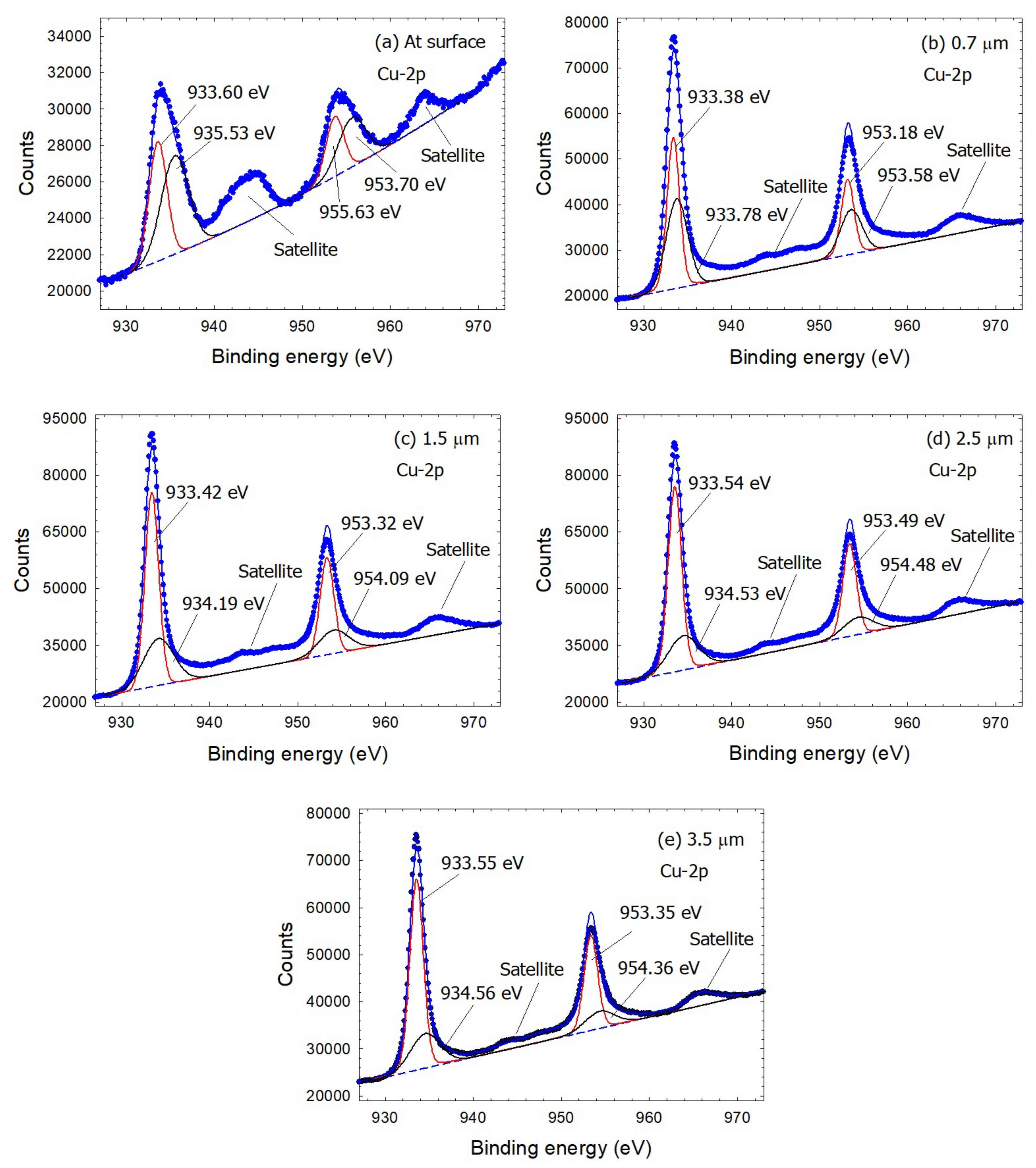
A clear image of the chemical bonds of these elements is possible by a deconvolution of peaks into individual lines. Figure 2 shows the XPS spectra of Cu-2p and the deconvolution into different sub-peaks. A linear background was subtracted, except for Figure 2a, where a quadratic background was employed. The deconvoluted XPS spectra of Cu-2p shows two sub-peaks for each of the Cu-2p3/2 (at ~933.5 eV) and Cu-2p1/2 (at ~955.5 eV) levels. Pure metallic copper (Cu(0)) appears at 932.7 eV for Cu-2p3/2 and at 952 eV for Cu-2p1/2 [22,23,24]. The left sub-peak (red line) of Cu-2p3/2 and Cu-2p1/2 is attributed to the metallic peak. The metal sub-peak gradually increases toward a larger depth of the film. The other sub-peak (blue line), which is assigned to metal oxide, decreases with a larger depth.
Each of the Cu-2p doublet peaks is followed by a satellite peak that gradually becomes weaker as one proceeds to a larger depth. The Cu satellite lines are attributed to copper oxide Cu(II)O [25]. The appearance of the Cu-2p satellite lines indicates the reactions of Cu with moisture (–OH radicals) during exposure to ambient air affecting only the top layers.
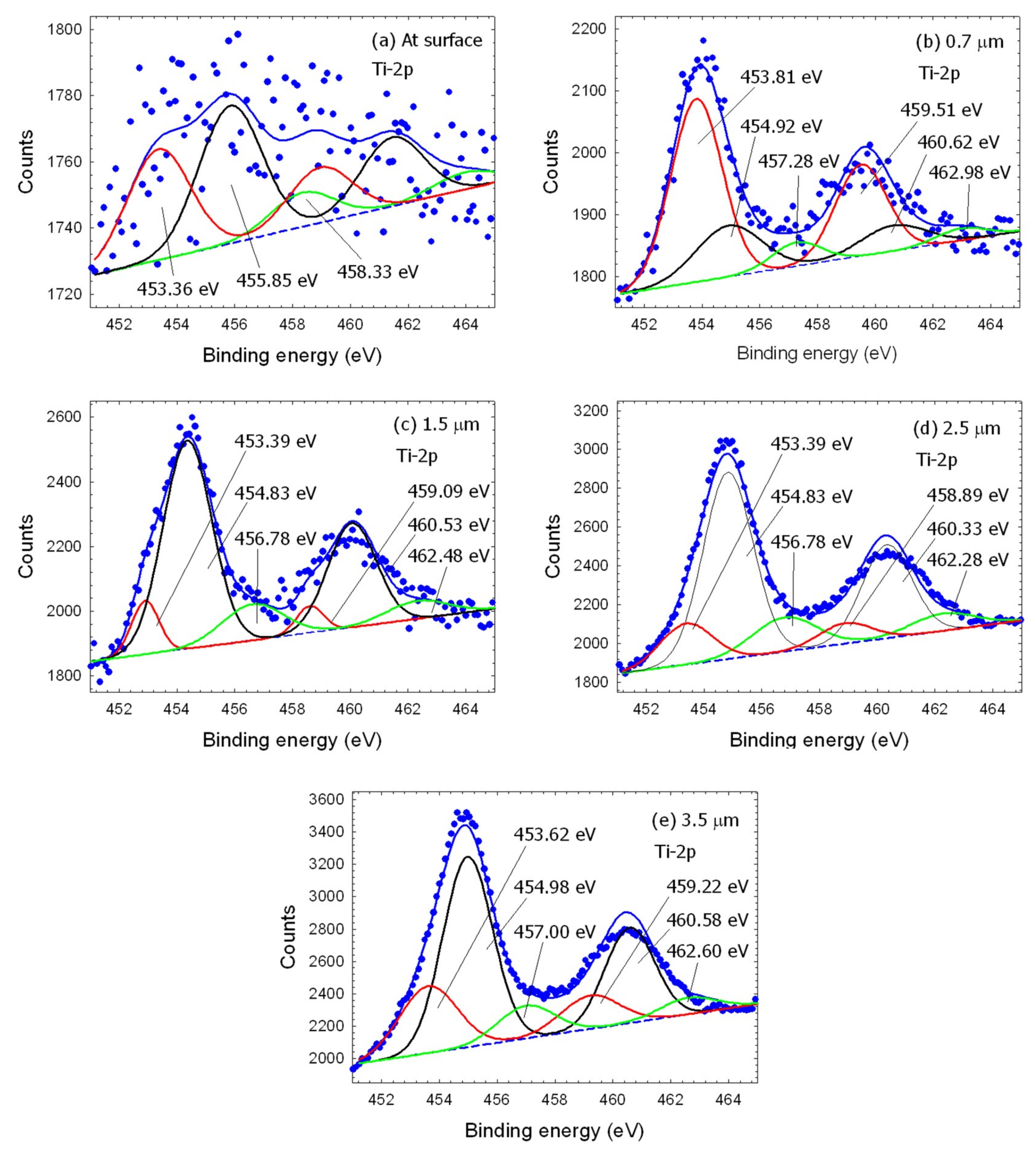
The XPS spectra of the Ti-2p are shown in Figure 3. It shows two main peaks at ~454.8 and ~461.2 eV for Ti-2p3/2 and Ti-2p1/2, respectively. Each peak is fitted with three components; the corresponding sub-peak energies for Ti-2p3/2 are ~453.5, 455.0, and 457.0 eV. The components could resemble TiC, Ti, and TiO with a Ti-2p3/2 binding energy of ~453.5, 454.9, and 457 eV, respectively [26]. The origin of the last component is not fully clear yet. Its energetic position is intermediate between TiO (Ti2+) and TiO2 (Ti4+, with a Ti-2p3/2 binding energy of ~459 eV), and it coincides with the energetic position of Ti3+ [27]. The surface spectrum (Figure 3a) displays a rather weak Ti-2p signal. In this particular case, the deconvolution into sub-peaks is of little significance due to the large scatter of the data points.
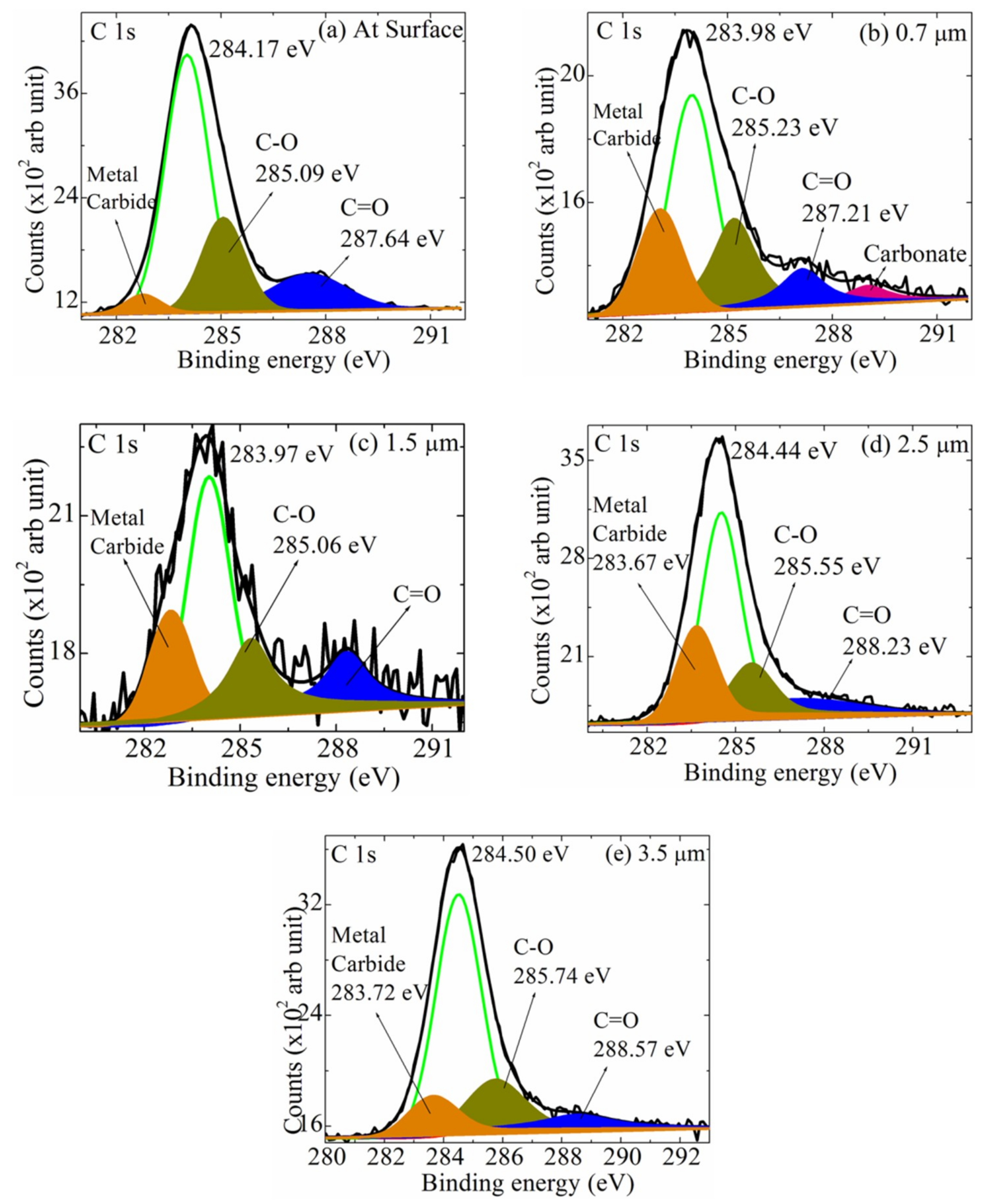
Figure 4 shows the C-1s core level XPS spectra. The deconvoluted sub-peaks are assigned to M-C (metal carbide), C–C, C–O, and C=O bonds [12,15,16]. A shift of −0.3 eV in C–C (or M-C) and 0.6 eV for C–O is observed at the top surface of the film. At a 2.5 μm depth, the chemical shift of the C–C bond is minimized (~0 eV) and amounts to about 1.1 eV for the C–O bond. One reason for is that the undesired oxygen amounts to only about 5% (whereas carbon amounts to 23%) at this depth, which is dominantly in a volatile state and not connected to a metal. The core level component of carbon with a binding energy of 284.5 eV is identified as originating from adventitious carbon. Similarly, the C-1s peak binding energy range at about 289 eV is identified as originating from CO type bonds, which depend on the type of bonding, such as ketones/aldehydes (–CO/–CHO) and carbonates (–CO3) [20,21,22].
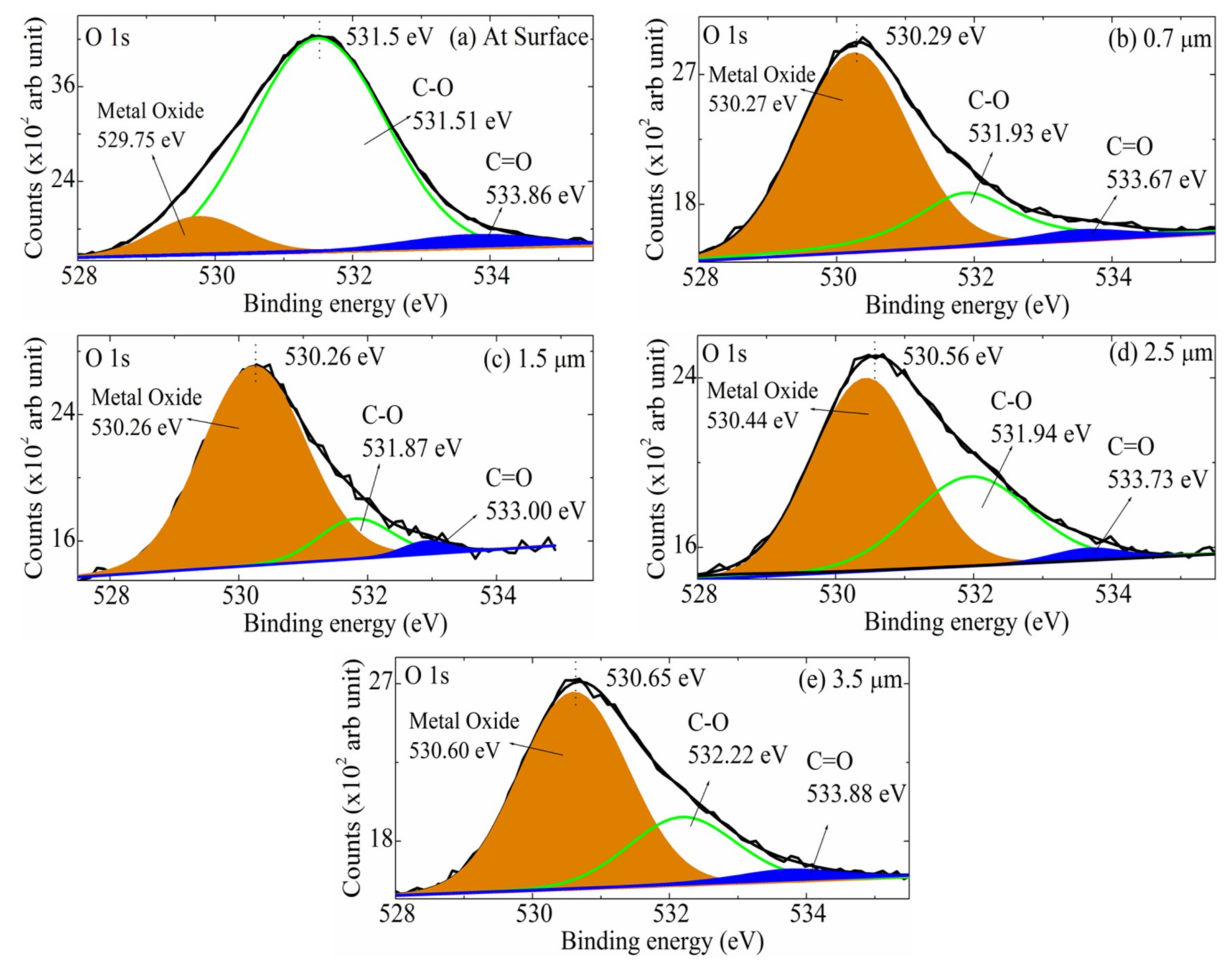
Figure 5 shows the de-convoluted O-1s spectra. It shows three sub-peaks at ~530, ~531.5, and ~533.5 eV, which are attributed to metal oxide, C–O, and C=O bonds, respectively [20,22].
The sub-peak at a lower binding energy indicates that oxygen is connected to a metal (metal oxide). Most oxygen at the surface is bound as C–O to, presumably, adventitious carbon. A common feature is observed in the O-1s spectra at a larger depth, where the oxygen component decreases and most of the remaining oxygen is bound as metal oxide.
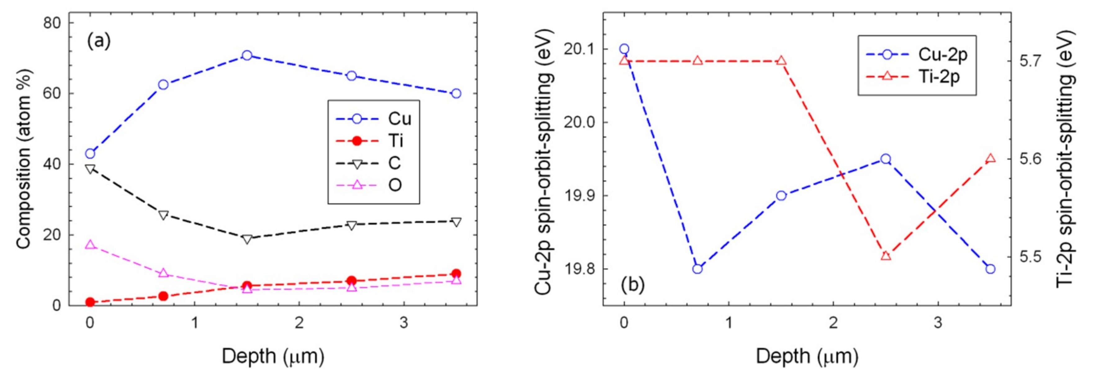
Figure 6a shows the relative composition (in at %) of Cu, Ti, C, and O, which amounts to 43%, 1%, 39%, and 17%, respectively, at the top surface of the film. At a depth of 1.5 μm, the relative composition of copper increases up to 71%, whereas the incorporated C and Ti are at 19% and 5.5%, respectively. The incorporated Cu, Ti, and C amount to 60%, 9% and 24%, respectively, at a depth of 3.5 μm. Carbon found on the surface is due to adsorption, and there is adventitious carbon with the C–C component of the C-1s peak at 284.6 eV. The incorporation of carbon is almost invariant at a depth of 1.5 μm to 3.5 μm, while Ti-2p increases gradually from 1% (surface) to 9% (3.5 μm).
We also investigated the spin-orbit-splitting between the 2p1/2 and 2p3/2 levels of Cu-2p andTi-2p. The reported values for the spin-orbit splitting range between 5.7–6.1 eV and 19.8–20.1 eV for Ti-2p and Cu-2p, respectively [26]. The present values of the Ti-2p and Cu-2p photoelectron spectra, which were derived from our best fits, are in the same range.
In general, the spin-orbit-splitting is considered constant and given by atomic structure theory. However, due to the chemical shift, which can differ for the 2p1/2 and 2p3/2 levels, small variations are not entirely unexpected. Our results seem to indicate that the spin-orbit-splitting is somewhat larger at the surface compared to inside the bulk, which could be explained by the different chemical composition. At present, the statistical accuracy does not allow for a clear conclusion, and further studies will be required to investigate this point.

3.2. TEM

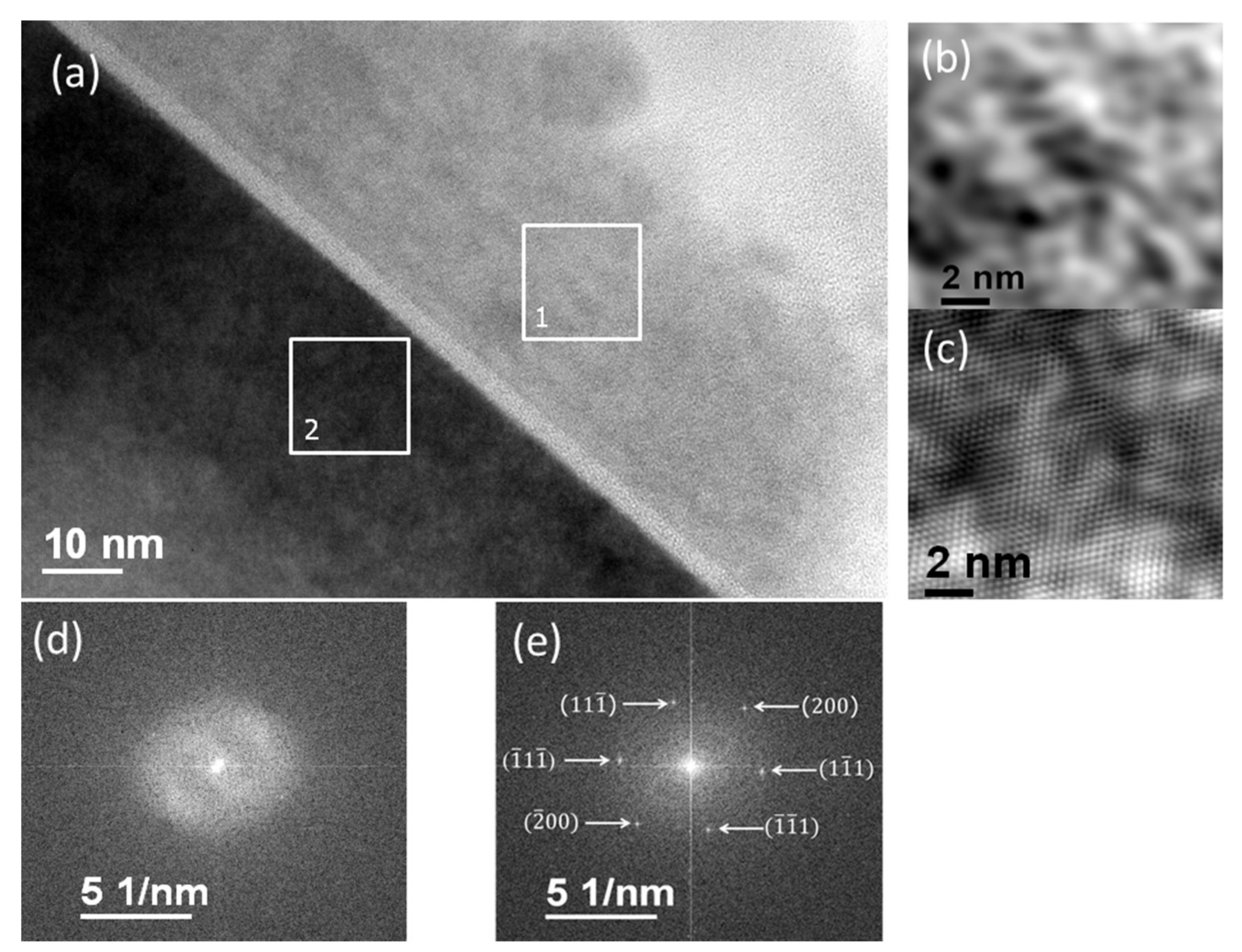
The crystalline structure of the deposited Cux–TiyCz film and of the Si substrate was investigated with the help of TEM (Figure 7). TEM images of the sample clearly show that the Si substrate is crystalline as we can observe its lattice structure (Figure 7c). First Fourier transform (FFT) analysis of the TEM images also implies these facts. The FFT image from region 1 which is on the Si substrate shows clear diffraction spots which confirms its crystalline nature whereas the FFT image produced from region 2 does not show any diffraction spots. On the other hand, we could not observe any lattice structure nor diffraction fringes of the Cux-TiyCz film (region 2). This seems to indicate that the deposited Cux-TiyCz film is amorphous in nature.

3.3. UV-VIS Spectra of Cux-TiyCz Film

The optical absorption is measured at five different depths (including the top surface) of the film. Figure 8 shows the optical band gap curve of the Cux–TiyCz films that is obtained from the absorption curves in the wavelength range from 300 to 900 nm. The absorption curve shows a linear trend with a long tail toward the minimum which can be characterised by two tangents. The point where the tangent of the absorption curve crosses the x-axis is used to determine the optical band gap. It suggests that the film has two band gaps, and the reason for this variation is due to the non-uniform composition at different depths of the film.
The optical band gap (considering the 1st tangential line) at the top surface is about 2.18 eV, whereas it is 2.09, 1.96, 1.83 and 2.00 eV for depths of 0.7, 1.5, 2.5 and 3.5 μm, respectively (Figure 8). At a higher film depth, the band gap energy decreases due to the reduction of oxygen and the increasing dominance of copper.
With increasing film depth the band gap energy decreases. We believe that it is caused by the reduction of oxygen and the increasing dominance of copper. The observed optical band gap is slightly larger compared to the 1.76 eV of copper oxide (CuO) which is a p-type semi-conductor [28]. The band gap of titanium oxide is significantly larger and not relevant here [29,30]. The optical band gap thus follows the trend of the deposited film composition at the surface as well as in the bulk of the film. In different depths it is observed that the unwanted oxygen is chemically bonded which plays a major role in increasing the dielectric constant of the material. At the surface oxygen amounts to 17%; it reduces to 4% and 5% at 1.5 and 2.5 μm depth, respectively. The decreasing oxygen content is in line with the decreasing Cu satellite line intensity which is attributed to copper oxide. TiC and CuC have different optical band gaps and definitely there are Ti-C and Cu-C phases involved in the formation of CuxTiyCz composite. But until now, there is no hypothetical prediction of CuxTiyCz material and it is a hard challenge to synthesize this material on a stoichiometric level. Moreover, the oxygen peaks result from the undesired absorption of moisture on the top of the film and the formation of an oxide layer of oxygen containing species.
The contamination is only on the surface and not in the bulk material. As a further assumption, a small fraction of carbon contamination could arise from adventitious carbon at the surface area. Again, the bulk is unaffected by adventitious carbon. However, at a certain depth of film, the conception of adventitious carbon does not fit. On this basis, we tried to correlate that the relative intensity of C% + O% might be roughly proportional to the spin-orbit splitting energy of Cu-2p.
There are three basic ways to enhance the incorporation of Ti and C during the growth and structural property of thin Cux–TiyCz films, i.e., the availability of carbon and titanium ions, a higher substrate temperature and a larger ion energy. In HiPIMS, the plasma density is larger by two to three orders of magnitude compared to DC magnetron discharges, with a large fraction of titanium and carbon (Ti and graphite targets) ionized species. Consequently, the flux of ions toward the substrate is large, which should enhance the growth of a smooth and dense film with a higher adhesion. The pulse operation during discharge improvises new parameters to control the deposition process, which can optimize the elemental composition in the deposited film [14]. One of the disadvantages of HiPIMS is that it offers a lower deposition rate and requires a more costly power supply.

4. Conclusions

Deposition of Cux–TiyCz films by co-sputtering in a magnetron plasma was demonstrated. Deposited films are analyzed as a function of film depth. The pronounced Cu peaks indicate the dominance of Cu in the bulk of the film compared to Ti and C. Cu and C with about 40% (at %) each dominate at the film surface where the O composition with 17% is also quite large. Ti composition with only 1% is small at the surface. The copper and titanium composition increase with increasing film depth reaching values of 60% and 9%, respectively, at a film depth of 3.5 μm. To the contrary, oxygen and carbon composition decrease with increasing film depth to 24% and 7% at 3.5 μm. At this depth the stoichiometric formula of the film is, hence, close to Cu7TiC3. TEM analysis shows that the deposited film is amorphous. The measured optical band gap amounts to 1.83 eV and 2.18 eV at 2.5 μm depth and at the surface of the film, respectively. It could make the film a useful material for solar energy applications. Our results show that co-sputtering in a magnetron discharge is a versatile technique for deposition of thin Cux–TiyCz films. As a ternary system, the deposited film may have interesting optical, electrical, and, due to the strong presence of Cu, anti-bacterial properties. Future projects have yet to investigate the dependence of film composition and properties on the plasma conditions, in particular, discharge power of each of the employed magnetrons.

Author Contributions

R.H. administered and supervised the experiment. S.C.D. and A.M. did the experiment. A.K.M., A.R., G.B., and A.M. analysed the experimental data. A.M. and R.H. wrote the paper.

Funding

This research was funded by the Deutsche Forschungsgemeinschaft (DFG) through Sonderforschungsbereich SFB/TRR24.

Conflicts of Interest

The authors declare no conflict of interest.

References

  1. Callister, W.D. Materials Science and Engineering: An Introduction; John Wiley & Sons: Hoboken, NJ, USA, 2007. [Google Scholar]
  2. Xu, X.; Li, W.; Wang, Y.; Dong, G.; Jing, S.; Wang, Q.; Feng, Y.; Fan, X.; Ding, H. Study of the preparation of Cu-TiC composites by reaction of soluble Ti and ball-milled carbon coating TiC. Results Phys. 2018, 9, 486–492. [Google Scholar] [CrossRef]
  3. Rathod, S.; Modi, O.; Prasad, B.; Chrysanthou, A.; Vallauri, D.; Deshmukh, V.; Shah, A. Cast in situ Cu–TiC composites: Synthesis by SHS route and characterization. Mater. Sci. Eng. A 2009, 502, 91–98. [Google Scholar] [CrossRef]
  4. Bagheri, G.A. The effect of reinforcement percentages on properties of copper matrix composites reinforced with TiC particles. J. Alloy. Compd. 2016, 676, 120–126. [Google Scholar] [CrossRef]
  5. Tjong, S.; Lau, K. Abrasive wear behavior of TiB2 particle-reinforced copper matrix composites. Mater. Sci. Eng. A 2000, 282, 183–186. [Google Scholar] [CrossRef]
  6. Akhtar, F.; Askari, S.J.; Shah, K.A.; Du, X.; Guo, S. Microstructure, mechanical properties, electrical conductivity and wear behavior of high volume TiC reinforced Cu-matrix composites. Mater. Charact. 2009, 60, 327–336. [Google Scholar] [CrossRef]
  7. Sapate, S.G.; Uttarwar, A.; Rathod, R.C.; Paretkar, R.K. Analyzing dry sliding wear behaviour of copper matrix composites reinforced with pre-coated SiCp particles. Mater. Des. 2009, 30, 376–386. [Google Scholar] [CrossRef]
  8. Buytoz, S.; Dagdelen, F.; Islak, S.; Kok, M.; Kir, D.; Ercan, E. Effect of the TiC content on microstructure and thermal properties of Cu–TiC composites prepared by powder metallurgy. J. Therm. Anal. Calorim. 2014, 117, 1277–1283. [Google Scholar] [CrossRef]
  9. Jha, P.; Gautam, R.K.; Tyagi, R.; Kumar, D. Sliding wear behavior of TiC-reinforced Cu-4 wt.% Ni matrix composites. J. Mater. Eng. Perform. 2016, 25, 4210–4218. [Google Scholar] [CrossRef]
  10. Sabbaghian, M.; Shamanian, M.; Akramifard, H.R.; Esmailzadeh, M. Effect of friction stir processing on the microstructure and mechanical properties of Cu–TiC composite. Ceram. Int. 2014, 40, 12969–12976. [Google Scholar] [CrossRef]
  11. Zhuang, J.; Liu, Y.; Cao, Z.; Li, Y. The influence of technological process on dry sliding wear behaviour of titanium carbide reinforcement copper matrix composites. Mater. Trans. 2010, 51, 2311–2317. [Google Scholar] [CrossRef]
  12. Yan, J.; Jiang, K.Y. Effects of process parameters on microstructure and properties of TiC reinforced Cu-matrix composites. Adv. Mater. Res. 2012, 557–559, 318–323. [Google Scholar] [CrossRef]
  13. Karadag, M.; Acikbas, G. Investigation of electrical and mechanical properties of Cu matrix TiC reinforced composites. Sch. J. Eng. Tech. 2018, 6, 58–63. [Google Scholar]
  14. Stranak, V.; Cada, M.; Hubicka, Z.; Tichy, M.; Hippler, R. Time-resolved investigation of dual high power impulse magnetron sputtering with closed magnetic field during deposition of Ti–Cu thin films. J. Appl. Phys. 2010, 108, 043305. [Google Scholar] [CrossRef]
  15. Helmersson, U.; Lattemann, M.; Bohlmark, J.; Ehiasarian, A.P.; Gudmundsson, J.T. Ionized physical vapor deposition (IPVD): A review of technology and applications. Thin Solid Film. 2006, 513, 1–24. [Google Scholar] [CrossRef] [Green Version]
  16. Bohlmark, J.; Lattemann, M.; Gudmundsson, J.; Ehiasarian, A.; Gonzalvo, Y.A.; Brenning, N.; Helmersson, U. The ion energy distributions and ion flux composition from a high power impulse magnetron sputtering discharge. Thin Solid Film. 2006, 515, 1522–1526. [Google Scholar] [CrossRef]
  17. Sarakinos, K.; Braun, A.; Zilkens, C.; Mráz, S.; Schneider, J.; Zoubos, H.; Patsalas, P. Exploring the potential of high power impulse magnetron sputtering for growth of diamond-like carbon films. Surf. Coat. Technol. 2012, 206, 2706–2710. [Google Scholar] [CrossRef] [Green Version]
  18. Aijaz, A.; Sarakinos, K.; Lundin, D.; Brenning, N.; Helmersson, U. A strategy for increased carbon ionization in magnetron sputtering discharges. Diam. Relat. Mater. 2012, 23, 1. [Google Scholar] [CrossRef]
  19. Stranak, V.; Wulff, H.; Rebl, H.; Zietz, C.; Arndt, K.; Bogdanowicz, R.; Nebe, B.; Bader, R.; Podbielski, A.; Hubicka, Z.; et al. Deposition of thin titanium–copper films with antimicrobial effect by advanced magnetron sputtering methods. Mater. Sci. Eng. 2011, C31, 1512–1519. [Google Scholar] [CrossRef]
  20. Moulder, J.F.; Stickle, W.F.; Sobol, P.E.; Bomben, K.D. Handbook of X-Ray Photoelectron Spectroscopy; Perkin-Elmer Corporation: Eden Prairie, MN, USA, 1992. [Google Scholar]
  21. Fiermans, L.; Vennik, J.; Dekeyser, W. Electron and Ion Spectroscopy of Solids; Plenum: New York, NY, USA, 1978. [Google Scholar]
  22. Wang, P.H.; Yap, P.S.; Lim, T.T. C–N–S tridoped TiO2 for photocatalytic degradation of tetracycline under visible-light irradiation. Appl. Catal. A 2011, 399, 252–261. [Google Scholar] [CrossRef]
  23. Majumdar, A.; Das, G.; Basvani, K.R.; Heinicke, J.; Hippler, R. Role of nitrogen in the formation of HC-N films by CH4/N2 barrier discharge plasma: Aliphatic tendency. J. Phys. Chem. B 2009, 113, 15734–15741. [Google Scholar] [CrossRef]
  24. Majumdar, A.; Drache, S.; Wulff, H.; Mukhopadhyay, A.K.; Bhattacharyya, S.; Helm, C.A.; Hippler, R. Strain effects by surface oxidation of Cu3N thin films deposited by DC magnetron sputtering. Coatings 2017, 7, 64. [Google Scholar] [CrossRef]
  25. Biesinger, M.C.; Lau, L.W.M.; Gerson, A.R.; Smart, R.S.C. Resolving surface chemical states in XPS analysis of first row transition metals, oxides and hydroxides: Sc, Ti, V, Cu and Zn. Appl. Surf. Sci. 2010, 257, 887–898. [Google Scholar] [CrossRef]
  26. NIST X-ray Photoelectron Spectroscopy Database. Available online: https://srdata.nist.gov/xps/ (accessed on 26 April 2019).
  27. Fu, Y.; Dua, H.; Zhang, S.; Huang, W. XPS characterization of surface and interfacial structure of sputtered TiNi films on Si substrate. Mater. Sci. Eng. 2005, A403, 25–31. [Google Scholar] [CrossRef]
  28. Chrysanthou, A.; Erbaccio, G. Production of copper-matrix composites by in situ processing. J. Mater. Sci. 1995, 30, 6339–6344. [Google Scholar] [CrossRef]
  29. Stranak, V.; Quaas, M.; Bogdanowicz, R.; Steffen, H.; Wulff, H.; Hubicka, Z.; Tichy, M.; Hippler, R. Effect of nitrogen doping on TiOxNy thin film formation at reactive high-power pulsed magnetron sputtering. J. Phys. D Appl. Phys. 2010, 43, 285203. [Google Scholar] [CrossRef]
  30. Stranak, V.; Cada, M.; Quaas, M.; Block, S.; Bogdanowicz, R.; Kment, S.; Wulff, H.; Hubicka, Z.; Helm, C.A.; Tichy, M.; Hippler, R. Physical properties of homogeneous TiO2 films prepared by high power impulse magnetron sputtering as a function of crystallographic phase and nanostructure. J. Phys. D: Appl. Phys. 2009, 42, 105204. [Google Scholar] [CrossRef]
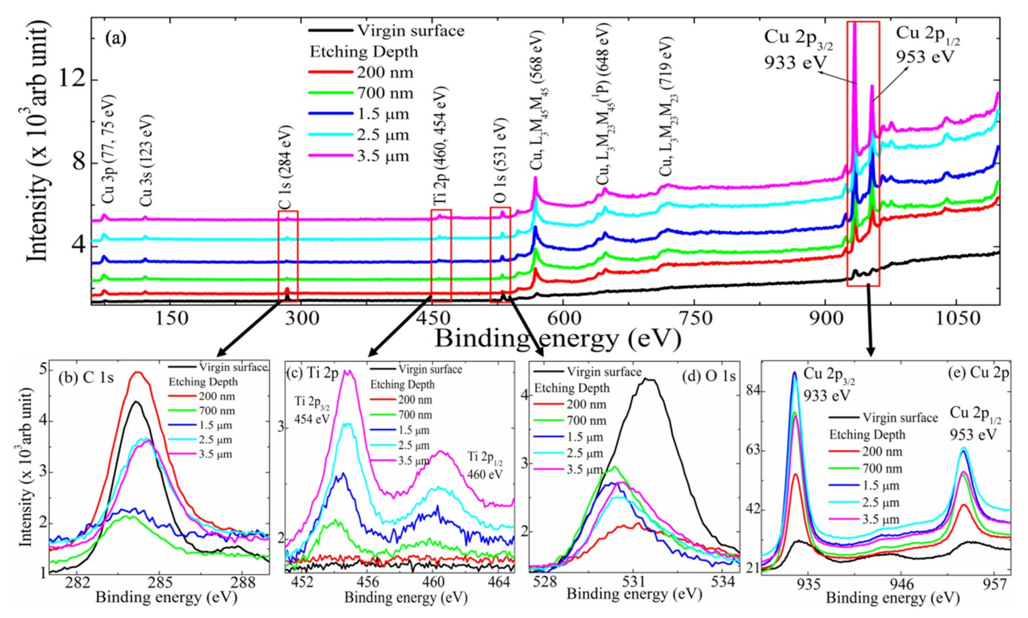
Figure 1. (a) Full scale (50 to 1050 eV) XPS spectrum of the as-deposited and etched Cux–TiyCz thin film. The red areas are magnified and shown separately in (b) C-1s, (c) Ti-2p, (d) O-1s and (e) Cu-2p. The XPS spectra were obtained with Al Kα x-rays, 23.5 eV pass energy, and 0.125 eV/step.
Coatings 09 00551 g001
Figure 2. The XPS spectra of the Cu-2p core peak of the Cux–TiyCz film at different depths: (a) at the surface, (b) 0.7 μm (c) 1.5 μm, (d) 2.5 μm, and (e) 3.5 μm. The blue solid lines resemble Gaussian fits with a linear background (dashed line), except for the surface spectrum where a quadratic background was used. The red and black lines represent metal and metal oxide sub-peaks, respectively. The intensity scales for the Cu-2p spectra are not the same.
Coatings 09 00551 g002
Figure 3. The Ti-2p XPS spectra of the Cux–TiyCz film at different depths: (a) at the surface, (b) 0.7 μm, (c) 1.5 μm, (d) 2.5 μm and (e) 3.5 μm. The blue solid lines resemble Gaussian fits. The red, black, and green lines represent the TiC, Ti, and TiO sub-peaks, respectively. The intensity scales for the Ti-2p spectra are not the same.
Coatings 09 00551 g003
Figure 4. The C-1s XPS spectra of the Cux–TiyCz film at different depths: (a) at the surface, (b) 0.7 μm (c) 1.5 μm, (d) 2.5 μm, and (e) 3.5 μm. The black solid lines resemble Gaussian fits. The orange, olive, and blue areas represent metal carbide, C–O, and C=O sub-peaks, respectively, and the green line shows C–C bonds. The intensity scales for the C-1s spectra are not the same.
Coatings 09 00551 g004
Figure 5. The O-1s core level XPS spectra of the Cux–TiyCz film at different depths: (a) at the surface, (b) 0.7 μm (c) 1.5 μm, (d) 2.5 μm and (e) 3.5 μm. The black solid lines resemble Gaussian fits. The orange and blue areas represent metal oxide and C=O sub-peaks, and the green line shows C–O bonds. The intensity scales for the O-1s spectra are not the same.
Coatings 09 00551 g005
Figure 6. (a) The relative composition (in %) of Cu, Ti, C, and O. The estimated accuracy is ±1 at %. (b) the spin-orbit splitting energy of Cu (2p3/2–2p1/2) and Ti (2p3/2–2p1/2), as a function of the film depth.
Coatings 09 00551 g006
Figure 7. (a) TEM image showing the investigated Cux–TiyCz film (1) and Si substrate (2) regions, (b) and (c) filtered high resolution TEM images, (d) and (e) diffraction pattern from regions 1 and 2, respectively.
Coatings 09 00551 g007
Figure 8. The absorption spectra of the Cux–TiyCz film deposited on the Si substrate films in the wavelength range from 300 to 900 nm: (a) at the surface, (b) 0.7 μm (c) 1.5 μm, (d) 2.5 μm and (e) 3.5 μm.
Coatings 09 00551 g008