Abstract
In this study, the operation method of the proposed ferroelectric memory structure as a method to overcome the limitations of the existing Charge Trap Flash (CTF) memory Vertical NAND (V-NAND) structure was presented and verified through device simulation. The proposed structure and operation method applied the BiCS (Bit Cost Scalable) structure GIDL (Gate Induce Drain Leakage) deletion method to confirm that selective program operation is possible in the ferroelectric memory V-NAND (Vertical Channel NAND) structure. In particular, we confirmed that the proposed method can easily suppress the program operation by adjusting the hole density of the channel even in the “Y-mode” operation. The channel hole density adjustment that makes this possible can be easily controlled by the voltage difference between the bit line (BL) and drain select line (DSL) contacts. The proposed structure was verified through a device simulation, and as a result of the verification, it was confirmed that the channel hole can be selectively charged in the program operation. Through this, when the cell to be programmed shows the program operation of 2.3 V, the other cells do not. It was confirmed that it could be suppressed to 0.4 V.
1. Introduction
The recent development of NAND flash technology for high density has been extensively utilized in industry. Since the first vertical channel NAND flash technology was announced by Toshiba in 2007 [1], the Terabit Cell Array Transistor (TCAT) by Samsung [2] and Stacked Memory Array Transistor (SMArT) by SK Hynix [3] were developed in 2009 based on this structure. Since then, the development of vertical channel structures has grown rapidly. In particular, the layered stack of the vertical channel structure is expected to have a high-end structure of more than 100 layers in 2019 [4,5,6].
Three-dimensional NAND memory is a high-density, cost-effective technology, but it still has some drawbacks such as speed, cell size, and power consumption at the system level due to the required peripherals (e.g., charge pump). In particular, the program speed is pointed out as a weak point compared to other memories (ex: DRAM) in the NAND flash structure, and attempts to solve this have been studied.
In order to solve this problem, next-generation memory that can replace the 3D-NAND memory of the ONO structure is being researched, and resistance change memory such as Phase-Change RAM (PCRAM), Resist-Change-RAM (RRAM), and Magnetic RAM (MRAM) has advantages such as relatively fast operating speed and low operating power [6]. Therefore, it was expected that such memory could replace the existing NAND flash memory. However, when the resistance change memories are configured as a large-scale product, the structure as well as the operation method is different from the existing NAND flash memory, and the 1Transistor-1Resistor (1T-1R) structure occupies a larger area than the 1T flash memory structure.
As a result of this problem, most of the resistance-changing memories studied so far do not replace mass storage devices such as Solid-State Disks (SSD) and have limited use in specialized fields such as internal memory. Among these, in the case of ferroelectric memory recently studied using HfO2 material [7,8,9,10,11,12], it is only necessary to replace the ONO structure used in the CTF flash with the ferroelectric material. Therefore, the NAND flash structure using the ferroelectric memory basically has an advantage that the existing NAND flash structure and operation method can be used as it is.
However, in the actual operation, since the operation of the ferroelectric memory is performed contrary to the CTF memory, a different operation method from the existing CTF memory is required. The most important difference is that the voltage that changes the threshold voltage of the memory cell in the positive direction is negative in the ferroelectric memory. This means that the channel, not the word line, must have a positive voltage when the ferroelectric memory performs a program operation.
However, unlike single devices, NAND strings are structurally unable to use sub-contacts. So, how to apply a positive voltage to the channel is just a way to apply a positive voltage to the BL or source line (SL). However, if a positive voltage is simply applied to the BL or SL, there is a problem that the voltage cannot be transmitted due to the characteristics of the silicon channel with high resistance. For this reason, a method of doping the channel itself with a high n-type has been proposed [9], but when this method is used, the threshold voltage of the proposed structure is located in the negative direction, so there is no memory window that can actually be used in the proposed structure. Therefore, in order to use ferroelectric memory in a V-NAND string structure, a method to solve this problem is essential. In addition, assuming multi-string operation, it is expected that selective program operation is not possible because all channels are always on in the proposed structure.
To solve this problem, in this paper, a new programming method using the BiCS (Bit Cost Scalable) GIDL (Gate Induce Drain Leakage) deletion method was proposed and verified through device simulation. As a result of the verification, if the proposed operation method is applied despite the inherent operation characteristics of ferroelectric memory, normal memory operation is possible while maintaining the existing V-NAND (Vertical Channel NAND) structure and wiring method. In addition, even in a multi-string operation, since it is possible to selectively generate GIDL only for the bit line (BL) to be programmed, the program operation is possible in the same manner as the existing V-NAND structure.
2. Details of the Proposed Structure and Operation
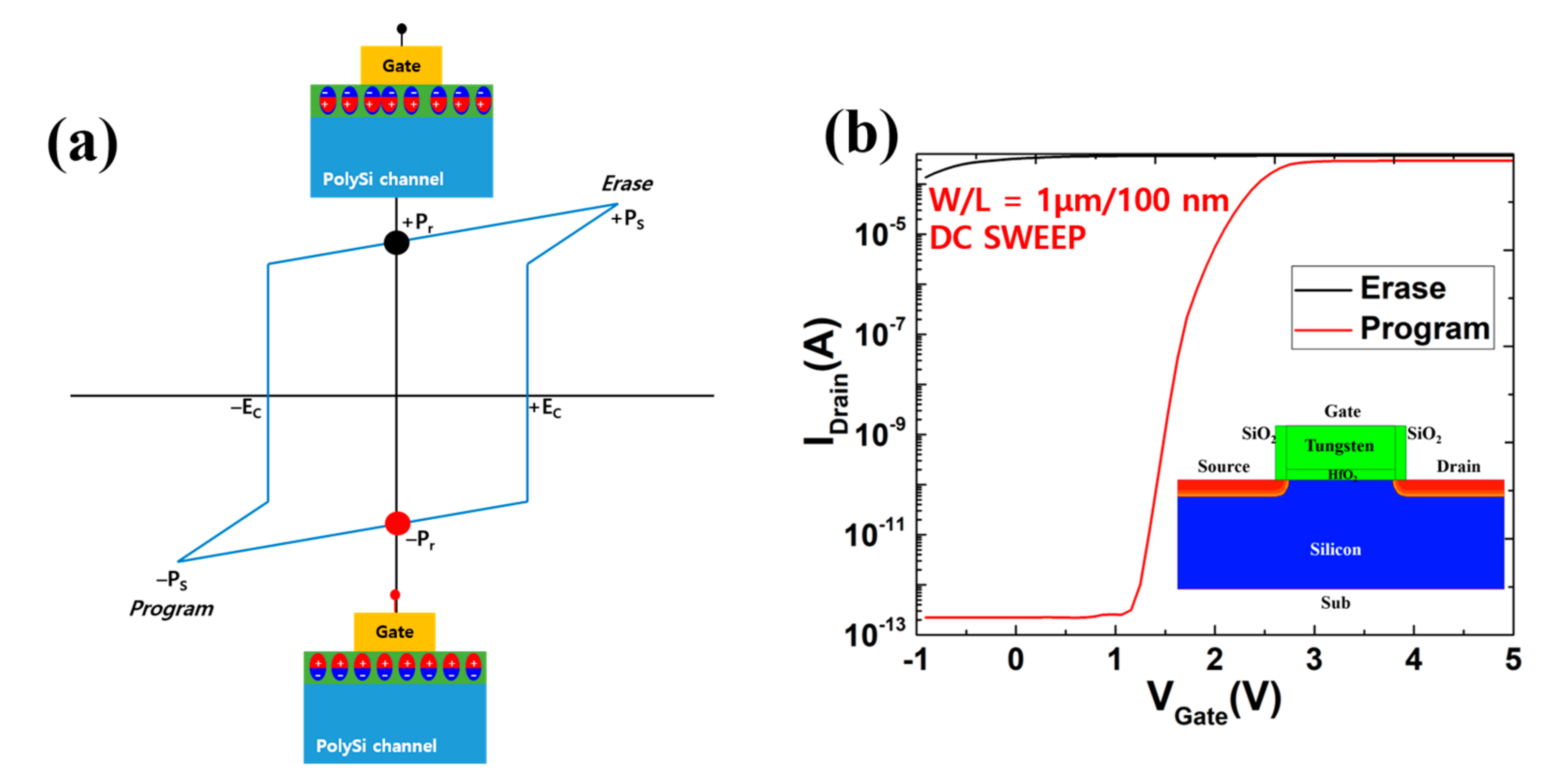
Figure 1 shows the operating characteristics of ferroelectric memory. As described above, the biggest feature of the ferroelectric memory is that the threshold voltage of the device moves in the negative direction when the gate voltage has a positive value and moves in the positive direction when the gate voltage has a negative value. Therefore, in the previous papers [6,7,8,9], operating with a positive value based on the gate voltage was described as a program operation, and operating with a negative value was described as an erase operation. However, in the case of such an operation criterion, there is a problem that the operation scheme in the actual read operation should be opposite to that of the existing CTF V-NAND because the resultant threshold voltage is the opposite the gate voltage. Therefore, in this paper, the criteria for program and erase operations are defined as the change in threshold voltage for each operation, not the gate voltage. Therefore, the program operation in this paper is that the gate voltage has a negative value, and as a result, the threshold voltage has a positive value, and the erase operation is the opposite.

Figure 1.
Shows the operating characteristics of ferroelectric memory. (a) describes the hysteresis curve of the ferroelectric memory and the corresponding operating characteristics, and (b) shows the operating characteristics in the 2D-FET.
Next, when using a ferroelectric memory structure in V-NAND, as described above, the gate voltage must be negative in the program operation. Therefore, in order to create such an environment, the channel should have a positive value and maintain the gate voltage in the ground state. However, since the V-NAND structure is that the sub-contact cannot be located inside the channel, the method to increase the channel voltage must transfer the positive voltage applied to the CSL or BL to the channel.
In order to increase the channel voltage in the V-NAND structure, a GIDL erase method or a bulk erase method used for an erase operation in an existing CTF structure can be used. In these methods, holes are commonly injected into the channel, and high voltages generated by CSL contacts located at the ends of the channel can be delivered to the channel through the holes present in the channel. In addition to this, unlike CTF’s erase operation, if only the word line (WL) that performs the program operation (the operation of changing the threshold voltage in the positive direction) remains in the ground state and the other WL maintains a moderately high voltage, an optional program may also be possible.
However, if the operation range is expanded to multiple string operations such as a real V-NAND structure rather than a single string, the program operation using the bulk erase method has a problem in that all strings sharing the same CSL are programmed in the existing structure [2]. In order to solve this problem, all of the lower Source Select Line (SSL) lines need to be separated, but such a change causes complexity of the operation line and thus has a disadvantage in that the manufacturing cost increases.
Therefore, it is appropriate to use the GIDL erase method of the BiCS structure for the program operation method of the ferroelectric memory, and the location generating the GIDL should be limited to the DSL adjacent to the BL. This is because SSL and CSL contacts are shared by all strings due to the structure of V-NAND as mentioned above.
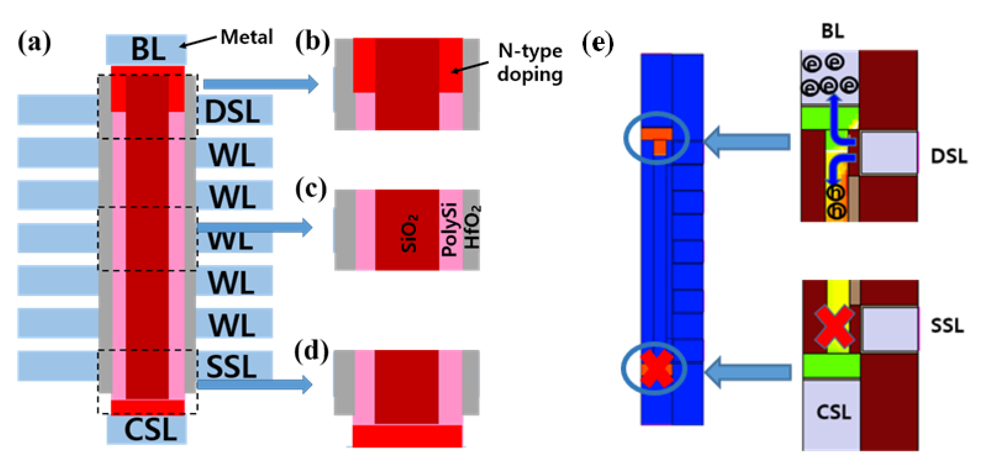
Figure 2 illustrates the structure proposed in this paper, and the basic structure is the same as the BiCS structure proposed by Toshiba. As shown in Figure 2a, the ONO layer, which is the storage layer, was changed to the HfO2 film, which is a ferroelectric insulating film. In addition, as shown in b and d of Figure 2, the drain select line (DSL) area has an over doping area that can generate GIDL, but the SSL area does not have such an over doping area. When the program operation proceeds in the structure designed in this way, GIDL occurs only in the DSL area, and the generated electrons escape to the BL contact to which the high voltage is applied, and only holes are charged in the channel. Therefore, the charged holes become carriers that transmit the high voltage of the BL contact. As shown in (e), when the program is operated with the designed structure, GIDL occurs only in the DSL area, and the generated electrons escape to the BL contact point where high voltage is applied, and only the hole is charged in the channel. Thus, the charged hole becomes the carrier carrying the high voltage of the BL contact.
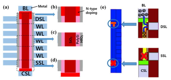
Figure 2.
Description of V-NAND structure of ferroelectric memory using Gate Induce Drain Leakage (GIDL) phenomenon. (a) shows the overall structure, (b) is a drain select line (DSL) transistor structure with an over-doped region for generating the GIDL phenomenon, (c) shows the word lines (WLs) region and (d) shows a Source Select Line (SSL) region without an over-doped region. Finally, (e) shows the movement of electrons and holes in the proposed GIDL program operation method.
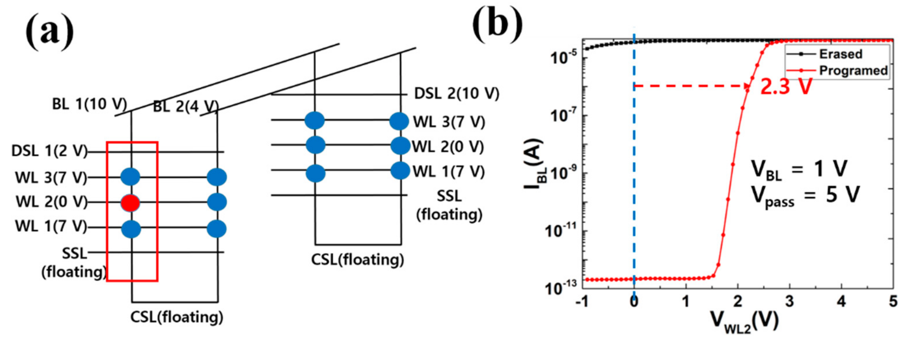
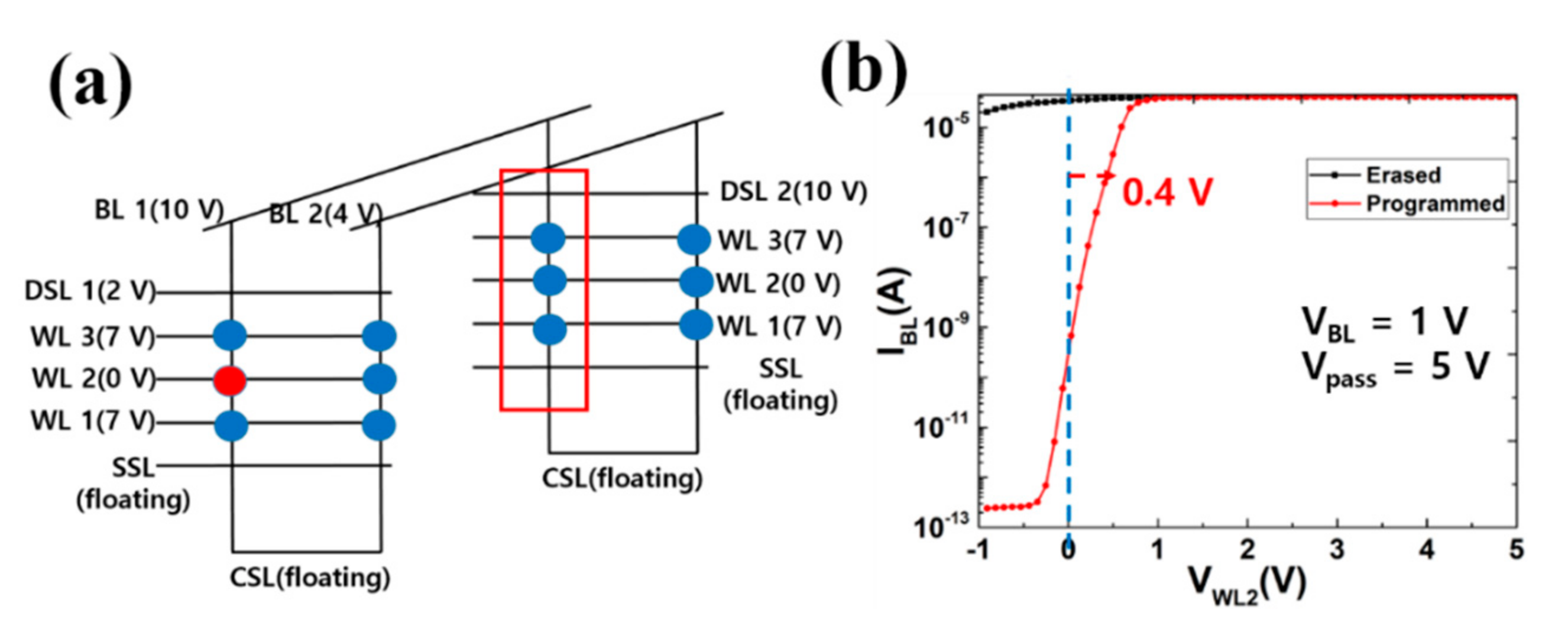
Figure 3 describes a plurality of string operations constructed based on the string structure described in Figure 2 above. When a target cell (red dot) is programmed in the normal V-NAND program operation, other cells (blue dots) should be able to suppress the program through the operation.

Figure 3.
Describe how the ferroelectric V-NAND structure operates in multiple string operations. (a) illustrates voltage distribution for programming only a specific cell in the combination of WL2 and BL1, and (b) describes the operating voltage of the contacts in each operation.
In the case of a string containing a cell to be programmed first, a high program voltage (VPROGRAM) is set for the BL of the string, and a low voltage is set for DSL (VDSL1). Through this operation, holes generated by the GIDL phenomenon occurring between the high N-type region connected to the BL and the DSL gate are transferred to the channel, and through these holes, the entire channel can maintain a high voltage. Next, when the WL to be programmed is maintained in the ground state (GND), polarization occurs in the HfO2 layer in the region where the WL is located due to a voltage difference from the channel. In addition, in the case of other WLs, since the difference between the applied pass voltage (VPASS) and the channel voltage is small, polarization can be suppressed (red square).
Next, in order to suppress the program operation of the same WL in the rear string sharing the same BL, the voltage of the DSL is increased (VDSL2), so that GIDL does not occur. In this case, no matter how high the voltage of the BL, there are no holes to transmit this voltage to the channel, so the voltage of the channel can be kept low (green square). Finally, in the case of strings using different BLs, the program can be loaded by keeping the BL voltage itself low (GND) (blue square).
Through a series of operations, the BiCS structured ferroelectric memory device using GIDL can perform the same program operation as when the existing CTF memory is applied.
3. Simulation Results and Discussion
In this study, we used the Sentaurus simulation tool from Synopsys [13] to form half of the vertical channel NAND structure section, as shown in Figure 2. In addition, this structure was employed as the virtual gate all (GAA) structure during device simulation through the cylindrical command (360 degree rotation) of the Sentaurus tool. Through this process, a complete vertical channel 3D NAND string was simulated.
This structure (Figure 4) comprises memory transistors named word line 1 (WL1), word line 2 (WL2) and word line 3 (WL3) along with top–bottom select transistors, namely, DSL and Source Select Line (SSL) transistors. Figure 2b shows an expanded view of the dimensions of the elements used in the simulated device. The total diameter of the simulation device is 100 nm. The word line gate length and the interval between successive word lines were fixed at 40 nm. In addition, the Metal Gate consists of a 2 nm thick TiN and a 36 nm Tungsten layer.
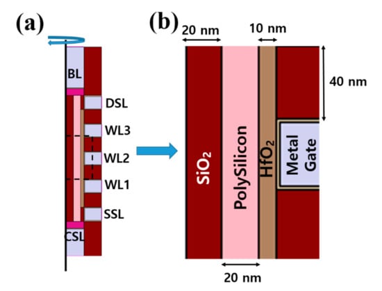
Figure 4.
Details of the simulated device. (a) Schematic of the three stacked memory cells, namely, word lines, WL1 to WL3, and select transistors, namely, SSL and DSL transistors, bit line (BL), and CSL. (b) Expanded view of the simulated structure with dimensions of the constituent parts.
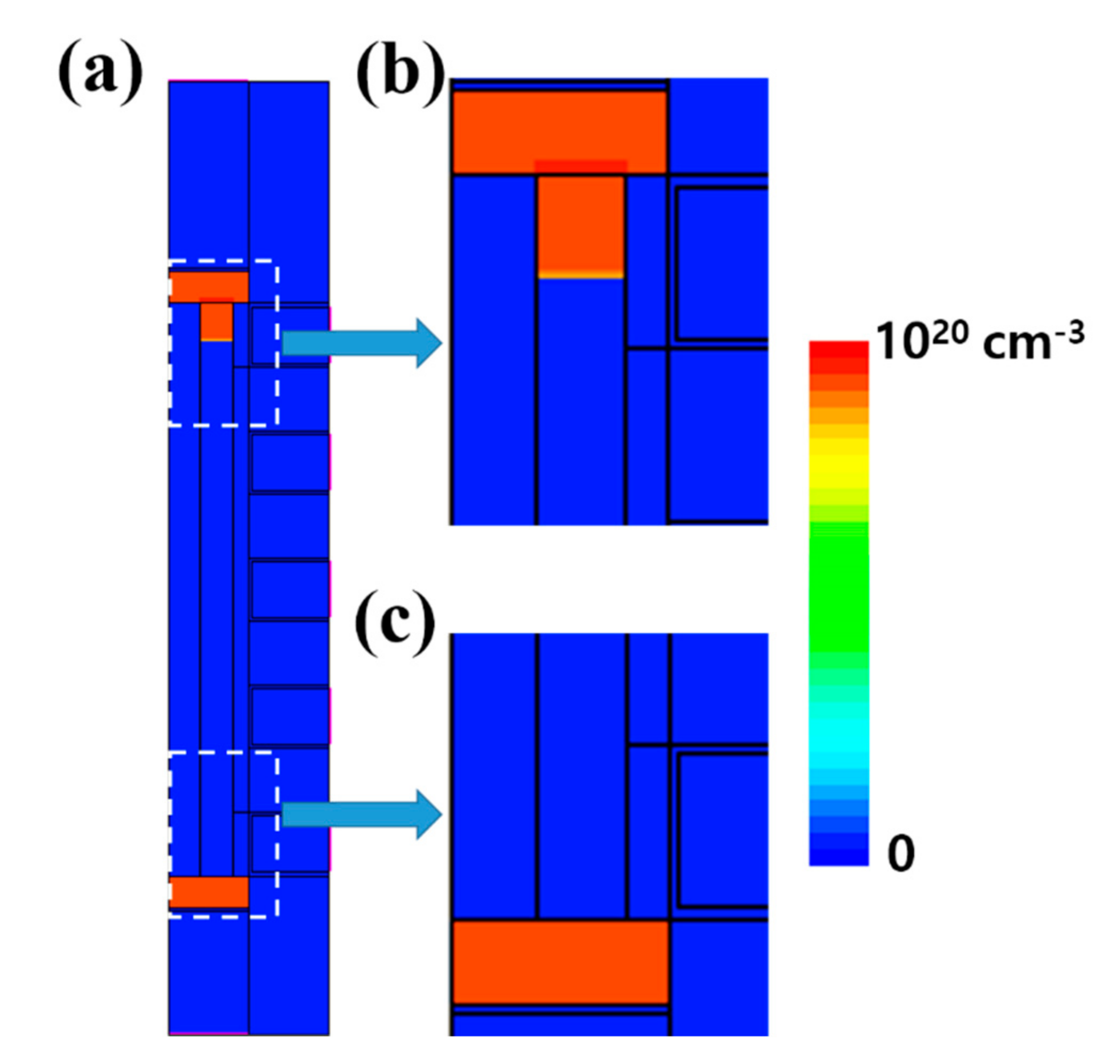
Figure 5 shows the doping state of the simulation structure. As described above, the excessive doping region for generating GIDL exists only in the DSL region and not in the SSL region. Therefore, channel boosting in the program operation can be selectively controlled according to the operation of the BL and DSL.
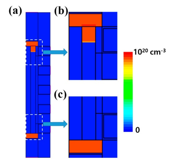
Figure 5.
Doping concentration. (a) shows the entire structure, (b) shows the expanded DSL area, and (c) shows the expanded SSL area.
In this study, the doping concentration dependence, high field saturation, trap scattering mobility and Trap-Assist-Tunnel (TAT) models were used in the given device simulations. In addition, Shockley-Read-Hall, Auger, Schenk band-to-band recombination, and tunneling models were also used to simulate the operation of V-NAND structure.
In addition, for each material trap, the parameters listed in Table 1 for polysilicon channel were applied. The parameters related to the polarization change of HfO2 are listed to Table 2.

Table 1.
Trap parameters of polysilicon channel.

Table 2.
Ferroelectric parameters of HfO2.
Figure 6 shows the operation result (Figure 6b) when the operating voltage of the simulation structure is set to program the WL2 cell of BL1 similar to the red square in (a). As expected, unlike the ref, the GIDL phenomenon caused by the 10 V voltage of BL and the 2 V voltage of DSL1 can maintain the voltage of the undoped polysilicon channel in a high voltage state, thereby showing a threshold voltage change of 2.3 V.

Figure 6.
Memory simulation results for program operation: (a) program operation voltage and (b) operation results.
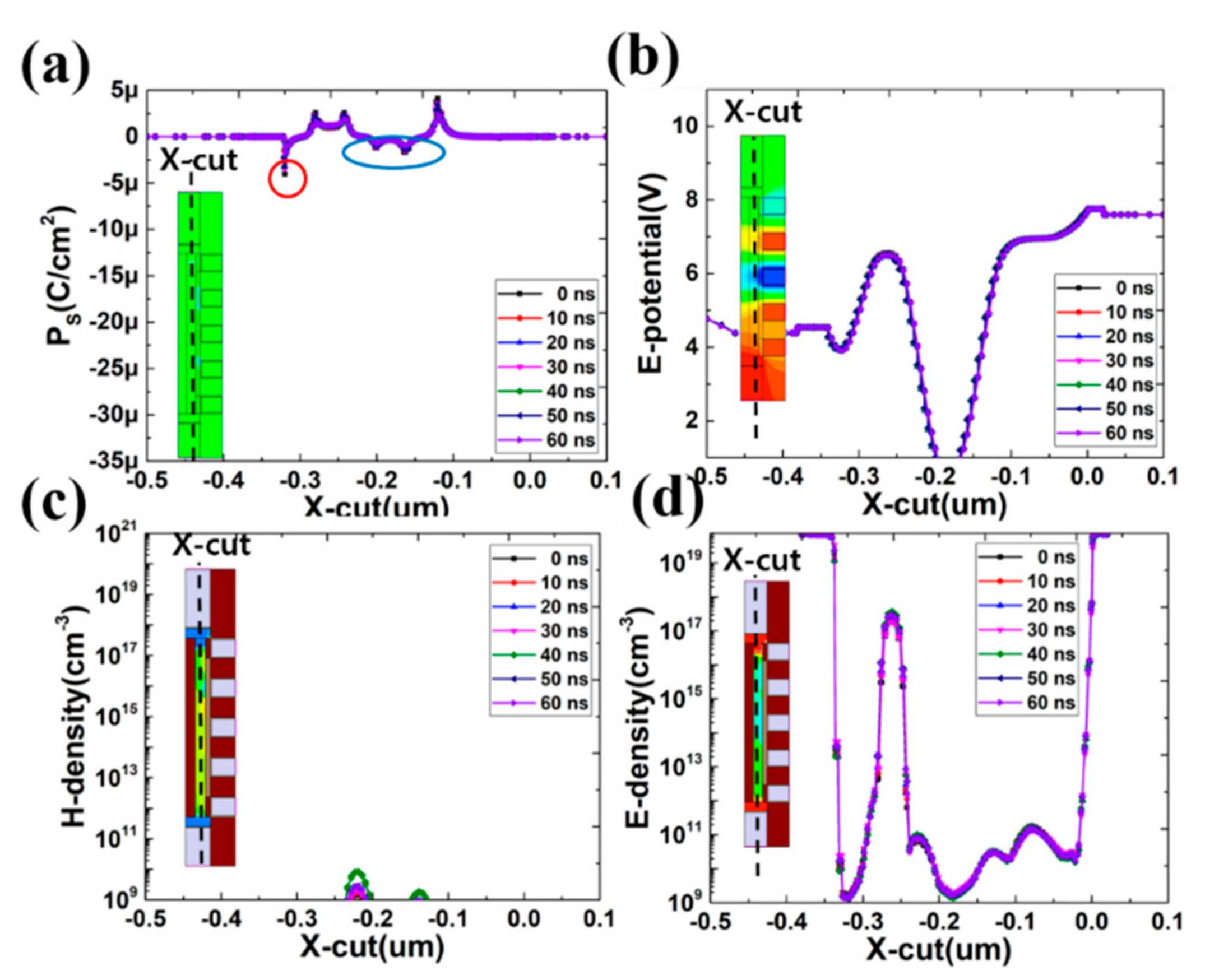
Figure 7 shows the various electrical changes that cause the threshold voltage changes identified in Figure 6. These changes are the amount of polarization (a), the potential of the channel (b), the hole density of the channel (c), and the electron density of the channel (d).
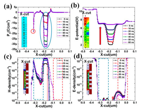
Figure 7.
Various electrical changes that cause a change in the threshold voltage in the program operation: (a) change in the amount of minuscule, (b) potential in the channel, (c) hole density in the channel, and (d) electron density in the channel.
First, it can be seen that the polarization amount change, which is a direct cause of the threshold voltage change, hardly changes at 0 ns and reaches the maximum polarization amount after 60 ns. However, since the change in polarization amount is linear, it is possible to assume that the delay of 60 ns is not the time itself for the polarization amount to change, but the voltage change in the channel is linear. This assumption can be confirmed in (b).
However, it has been confirmed that this program operation causes an unintended change in the amount of polarization between DSL and WL3 (red circle) along with a change in the amount of polarization in WL2 (blue circle). This unintended change in polarization can cause a soft program problem that occurs even in the existing CTF memory structure, so if the ferroelectric memory does not have a sufficient EC value, one or two WL adjacent to the DSL can be used as a dummy cell.
Figure 7b shows the change in channel voltage that caused the change in polarization amount. As mentioned above, it can be seen that the change of the channel voltage hardly changes at 0 ns and rises linearly for 60 ns. In addition, the channel voltage at the time of reaching the maximum polarization amount is 7 V, which shows that 3 V is reduced compared to 10 V applied from BL. This change is because, unlike the structure proposed in ref [9], holes are injected into the undoped pure polysilicon channel to operate. Therefore, it should be considered that the voltage of the actual channel may be reduced to a certain level depending on the concentration of the injected hole and the electrical state of the polysilicon channel.
Figure 7c shows the change in hole density that causes the change in channel voltage. In the case of holes existing in the channels from DSL to WL 2, it can be seen that they are generated by the GIDL phenomenon generated in DSL and transferred to WL2. The density of holes transferred in this way has the highest value of 1021 cm−3 near WL2, which is 0 V, and in the case of WL3, which is Vpass, it is less than 1014 cm−3 to 1016 cm−3, but it can be seen that voltage transmission is possible. Conversely, the hole density from WL2 to CSL is 109 cm−3 or less, and there is virtually no hole. These results can be thought of as the transmitted hole is attracted to the low voltage of WL2 and cannot be transmitted down the WL2.
The depletion of the hole concentration is small enough that WL1 applied with the Vpass voltage below WL2 cannot perform self-boosting operation [11,12], but on the contrary, it can be seen that the electron concentration is about 1011 cm−3, as shown in Figure 7d. These results can be thought of as the surrounding electrons pushed by the low voltage of WL2 being attracted to the Vpass voltage of WL1, and by these electrons, WL1 can maintain the channel voltage by self-boosting operation and prevent unintended program operation. As a result, it can be seen that the amount of polarization change of each WL in the program operation has little change in the polarization amount of the pass states WL1 and WL3 except for the program state WL2 as shown in (a).
Figure 8 shows the operating voltage configuration (a) and the resulting operation (b) to suppress the program operation of the same WL2 in the string connected to BL2. As expected, the proposed operation changed the threshold voltage change of WL2 to only 0.4 V.
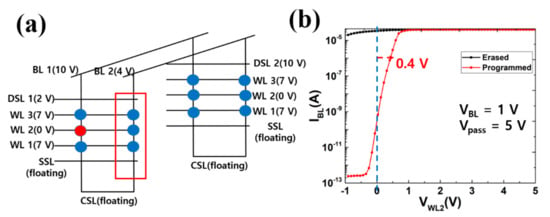
Figure 8.
Memory simulation results for program operation: (a) program operation voltage and (b) operation results.
First, the change in polarization amount, which is a direct cause of the threshold voltage change, changed only up to −3u C/cm2, unlike the results in Figure 7, and the change in this level cannot change the threshold voltage. Therefore, the threshold voltage of all WLs was suppressed to 0.4 V, as shown in Figure 8. Next, it can be seen that the change in channel voltage is also self-boosted according to changes in WLs, unlike in Figure 7b. In particular, in the case of WL2 in the 0 V state for program operation, the channel voltage also becomes 0 V, and the program operation is suppressed. In the case of Figure 7c showing the change in hole density, since the voltage applied to the BL is 4 V, GIDL does not occur at this voltage, so it can be seen that the channel is maintained in a state without holes. Therefore, the voltage state of the channel depends on the electron density shown in Figure 7d. At this time, a self-boosting operation occurs according to the voltage state of each WL, and through this, the difference between the channel voltage and the WL voltage can be suppressed. As a result, the proposed operation mode in other strings with low BL voltage can successfully control the program operation of all WLs including WL2.
Figure 9 shows the various electrical changes that cause the low threshold voltage changes identified in Figure 8. These changes are the amount of polarization (a), the potential of the channel (b), the hole density of the channel (c), and the electron density of the channel (d).

Figure 9.
Various electrical changes that suppress the threshold voltage change in the program suppression operation: (a) change in the amount of minuscule, (b) potential in the channel, (c) hole density in the channel, (d) electron density in the channel.
Figure 10 shows the operating voltage configuration (a) and the resulting operation (b) to suppress the program operation of the same WL2 in the string connected to BL1. In this string, since the same BL1 is shared, to suppress the GIDL phenomenon, a method of reducing the voltage difference between the two contacts by increasing the voltage of DSL2 to the same level as BL must be used. As a result, as shown in (b), the change in threshold voltage of WL2 could be suppressed to 0.4 V. In particular, in the existing V-NAND structure, the above string position is called “Y-mode” [14,15], and it is known to control by applying a fine step self-boosting operation to suppress the program operation. However, the ferroelectric memory structure shows that the program operation can be sufficiently suppressed by simple voltage regulation.
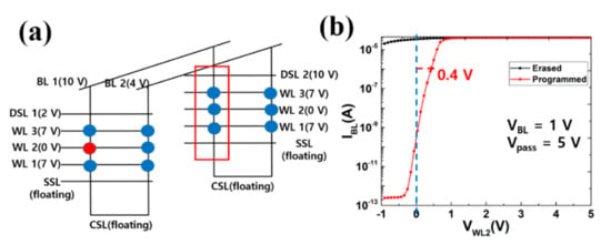
Figure 10.
Memory simulation results for program operation: (a) program operation voltage and (b) operation results.
Figure 11 shows the various electrical changes that cause the low threshold voltage changes identified in Figure 10. These changes are the amount of polarization (a), the potential of the channel (b), the hole density of the channel (c), and the electron density of the channel (d). First, the change in polarization amount, which is a direct cause of the threshold voltage change, changed only up to 3u, unlike the results in Figure 7, and the change in this level cannot change the threshold voltage. Therefore, the threshold voltage of all WLs was suppressed to 0.4 V, as shown in Figure 10. In addition, these results proved that the program operation can be suppressed while sharing the high voltage of 10 V of BL1.
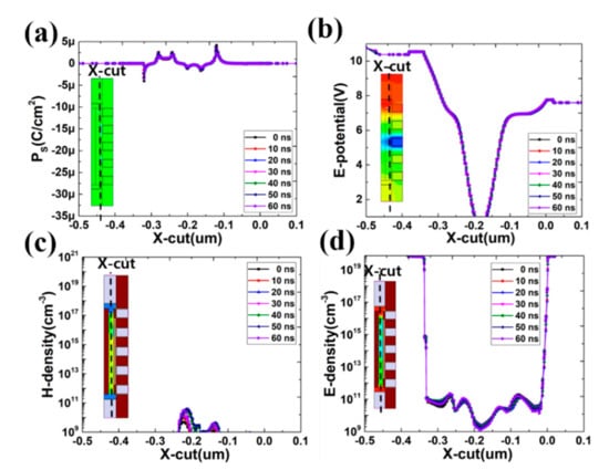
Figure 11.
Various electrical changes that suppress the threshold voltage change in the program suppression operation (Y-mode): (a) change in the amount of minuscule, (b) potential of the channel, (c) hole density of the channel, (d) electron density of the channel.
The change in channel voltage shown in Figure 11b does not cause the GIDL phenomenon by matching 10 V the voltages of the BL and DSL contacts as described above. Therefore, when using the proposed structure and operation method, the ferroelectric V-NAND structure shows that the operation in “Y-mode”, which is known to be the most vulnerable in the existing CTF structure V-NAND, can also accurately suppress the program operation.
Table 3 shows the results of comparing the proposed structure with the currently used CTF V-NAND structure and the previously announced structure using the N-type polysilicon channel. First, in terms of the memory window, the proposed structure is still smaller than that of the CTF V-NAND structure, but unlike the N-type channel structure, a positive memory window can be reliably secured. This fact can be expected to show performance beyond CTF V-NAND reliably if additional memory windows are secured with the development of ferroelectric materials in the future. On the contrary, in terms of energy used for program operation, the proposed structure uses less energy than the CTF-V-NAND structure, but it is used basically intrinsic polysi channel, so it needs the energy required for the GIDL operation. Therefore, the proposed structure should use more energy than the N-type channel structure that does not require an additional carrier. However, since the energy used in the proposed structure is mostly used for the GIDL operation and very little energy is used for the actual program operation [8], it can be expected to be clearly less than the CTF V-NAND structure.

Table 3.
Performance comparison of published ferroelectric V-NAND structures.
4. Conclusions
In this study, an operation method of the proposed ferroelectric memory structure was proposed as a method to overcome the limitations of the existing CTF memory V-NAND structure and verified through device simulation. The proposed structure and operation method showed that by applying the BiCS structure GIDL erasing method, the ferroelectric memory V-NAND structure can be operated by changing the operation method without additional processes such as channel doping, unlike the method proposed in other studies. As a result of verifying the proposed structure and operation method through device simulation, it was confirmed that the cell in which the program operation was performed shows a memory window of 2.3 V, but the cells whose program operation was inhibited were suppressed to 0.4 V. These results show that the GIDL phenomenon can be effectively controlled according to the voltage combination of BL and DSL in the DSL area of the proposed structure, and it is possible to effectively control the holes and voltage in the channel according to the control of this GIDL phenomenon.
Author Contributions
Methodology, paper writing, investigation, conceptualization, Validation, writing, investigation, S.C. Review, C.C., M.K. and J.K.J. Funding acquisition, supervision, editing, Y.-h.S. All authors have read and agreed to the published version of the manuscript.
Funding
This research received no external funding.
Acknowledgments
This research was supported by Samsung Research Funding & Incubation Center of Samsung Electronics under Project Number SRFC-TA1903-04. Also, it was supported by the Ministry of Trade, Industry & Energy (MOTIE (project number 20003808)) and Korea Semiconductor Research Consortium (KSRC) support program for the development of the future semiconductor device.
Conflicts of Interest
The authors declare no conflict of interest.
References
- Tanaka, H.; Kido, M.; Yahashi, K.; Oomura, M.; Katsumata, R.; Kito, M.; Fukuzumi, Y.; Sato, M.; Nagata, Y.; Matsuoka, Y.; et al. Bit Cost Scalable Technology with Punch and Plug Process for Ultra High Density Flash Memory. In Proceedings of the 2007 IEEE Symposium on VLSI Technology, Kyoto, Japan, 12–14 June 2007; pp. 14–15. [Google Scholar]
- Jang, J.; Kim, H.S.; Cho, W.; Cho, H.; Kim, J.; Shim, S.L.; Jeong, H.; Son, B.K.; Kim, D.W.; Shim, J.J.; et al. Vertical Cell Array usingTCAT(Terabit Cell Array Transistor) Technology for UltraHigh Density NAND Flash Memory. In Proceedings of the 2009 Symposium on VLSI Technology, Honolulu, HI, USA, 15–17 June 2009; pp. 192–193. [Google Scholar]
- Choi, E.S.; Park, S.K. Device Considerations for High Density and Highly Reliable 3D NAND Flash Cell in Near Future. In Proceedings of the 2012 International Electron Devices Meeting, San Francisco, CA, USA, 10–13 December 2012; pp. 211–214. [Google Scholar]
- TechInsights Memory Technology Update from IEDM18. 11 April 2019. Available online: https://www.techinsights.com/blog/techinsights-memory-technology-update-iedm18 (accessed on 27 December 2020).
- Johann, A.; Higashitani, M.; Paak, S.S.; Sivaram, S. Past and Future of 3D Flash. In Proceedings of the 2020 IEEE International Electron Devices Meeting (IEDM), Virtually, San Francisco, CA, USA, 12–18 December 2020; pp. 103–106. [Google Scholar]
- International Roadmap for Devices and Systemstm 2018 Update More Moore. August 2018. Available online: https://irds.ieee.org/images/files/pdf/2018/2018IRDS_MM.pdf (accessed on 11 December 2020).
- Trentzsch, M.; Flachowsky, S.; Richter, R.; Paul, J.; Reimer, B.; Utess, D.; Jansen, S.; Mulaosmanovic, H.; Müller, S.; Slesazeck, S.; et al. A 28 nm HKMG super low power embedded NVM technology based on ferroelectric FETs. In Proceedings of the 2016 IEEE International Electron Devices Meeting (IEDM), San Francisco, CA, USA, 3–7 December 2016; pp. 217–294. [Google Scholar]
- Dünkel, S.; Trentzsch, M.; Richter, R.; Moll, P.; Fuchs, C.; Gehring, O.; Majer, M.; Wittek, S.; Müller, B.; Melde, T.; et al. A FeFET based super-low-power ultra-fast embedded NVM technology for 22 nm FDSOI and beyond. In Proceedings of the 2017 IEEE International Electron Devices Meeting (IEDM), San Francisco, CA, USA, 2–6 December 2017; pp. 486–488. [Google Scholar]
- Ni, K.; Smith, J.; Ye, H.; Grisafe, B.; Bruce, R.G.; Kummel, A.; Datta, S. A Novel Ferroelectric Superlattice Based Multi-Level Cell Non-Volatile Memory. In Proceedings of the 2019 IEEE International Electron Devices Meeting (IEDM), San Francisco, CA, USA, 7–11 December 2019; pp. 669–672. [Google Scholar]
- Florent, Y.K.; Pesic, M.; Subirats, A.; Banerjee, K.; Lavizzari, S.; Arreghini, A.; Piazza, L.D.; Potoms, G.; Sebaai, F.; McMitchell, S.R.C.; et al. Vertical Ferroelectric HfO2 FET based on 3-D NAND Architecture: Towards Dense Low-Power Memory. In Proceedings of the 2018 IEEE International Electron Devices Meeting (IEDM), San Francisco, CA, USA, 1–5 December 2018; pp. 43–46. [Google Scholar]
- Mo, F.; Tagawa, Y.; Jin, C.; Ahn, M.; Saraya, T.; Hiramoto, T.; Kobayashi, M. Experimental Demonstration of Ferroelectric HfO2 FET with Ultrathin-body IGZO for High-Density and Low-Power Memory Application. In Proceedings of the 2019 Symposium on VLSI Technology, Kyoto, Japan, 9–14 June 2019; pp. 42–43. [Google Scholar]
- Ku, B.C.; Choi, S.J.; Song, Y.; Choi, C.H. Fast Thermal Quenching on the Ferroelectric Al:HfO2 Thin Film with Record Polarization Density and Flash Memory Application. In Proceedings of the 2020 Symposium on VLSI Technology, Kyoto, Japan, 16–19 June 2020; pp. 14–15. [Google Scholar]
- Sentaurus Device User Guide; Version J-2014.9; Synopsys: Research Triangle Park, NC, USA, 2014.
- Shim, K.; Choi, E.; Jung, S.; Kim, S.; Yoo, H.; Jeon, K.; Joo, H.; Oh, J.; Jang, Y.; Park, K.; et al. Inherent Issues and Challenges of Program Disturbance of 3D NAND Flash Cell. In Proceedings of the IEEE International Memory Workshop, Milan, Italy, 20–23 May 2012; pp. 1–4. [Google Scholar]
- Yoo, H.; Choi, E.; Oh, J.; Park, K.; Jung, S.; Kim, S.; Shim, K.; Joo, H.; Jung, S.; Jeon, K.; et al. Modeling and Optimization of the Chip Level Program Disturbance of 3D NAND Flash Memory. In Proceedings of the IEEE International Memory Workshop, Monterey, CA, USA, 26–29 May 2013; pp. 1–4. [Google Scholar]
Publisher’s Note: MDPI stays neutral with regard to jurisdictional claims in published maps and institutional affiliations. |
© 2020 by the authors. Licensee MDPI, Basel, Switzerland. This article is an open access article distributed under the terms and conditions of the Creative Commons Attribution (CC BY) license (http://creativecommons.org/licenses/by/4.0/).

