Design and Implementation of Fast Locking All-Digital Duty Cycle Corrector Circuit with Wide Range Input Frequency


Abstract
:1. Introduction
2. Circuit Description
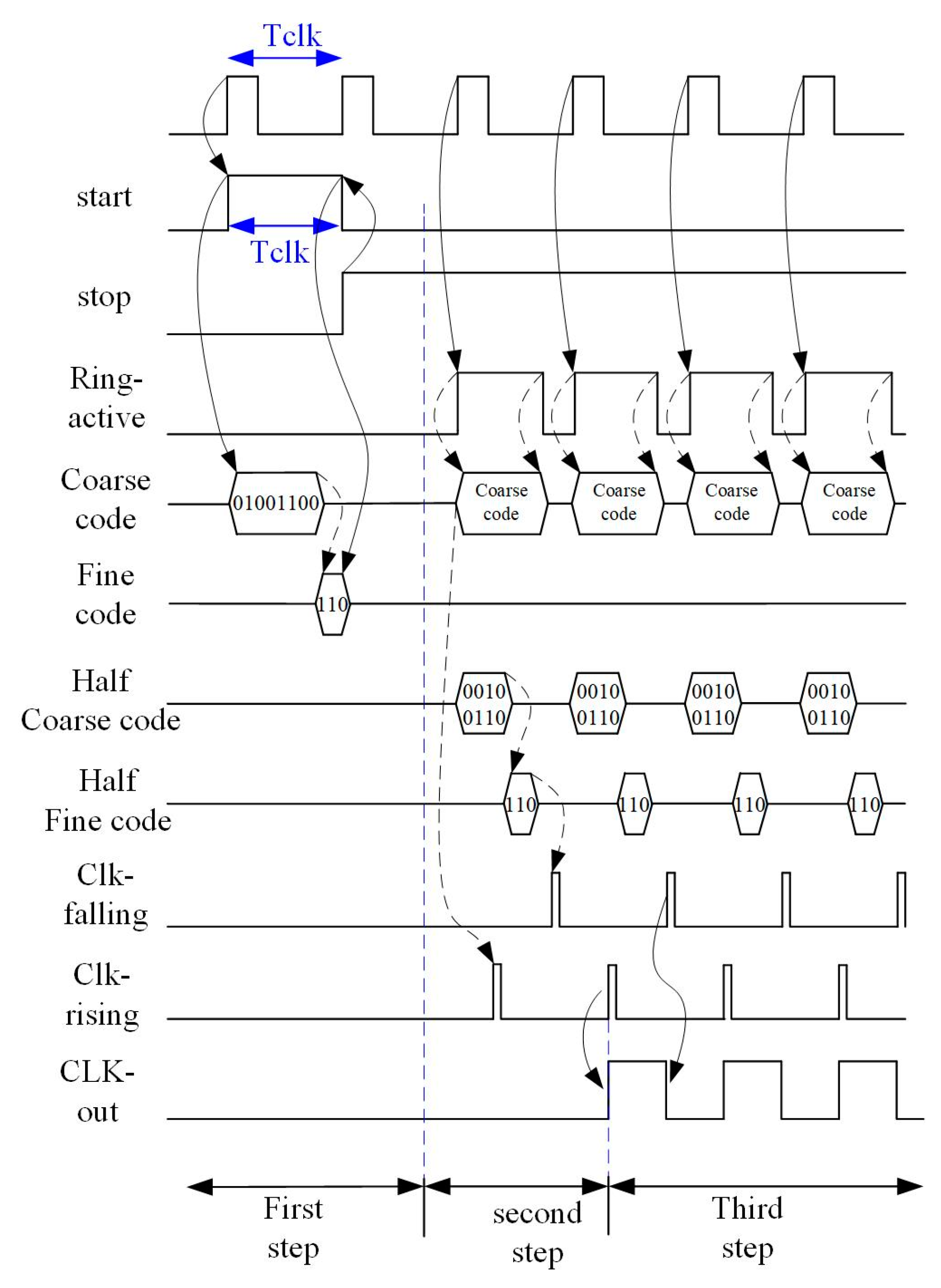
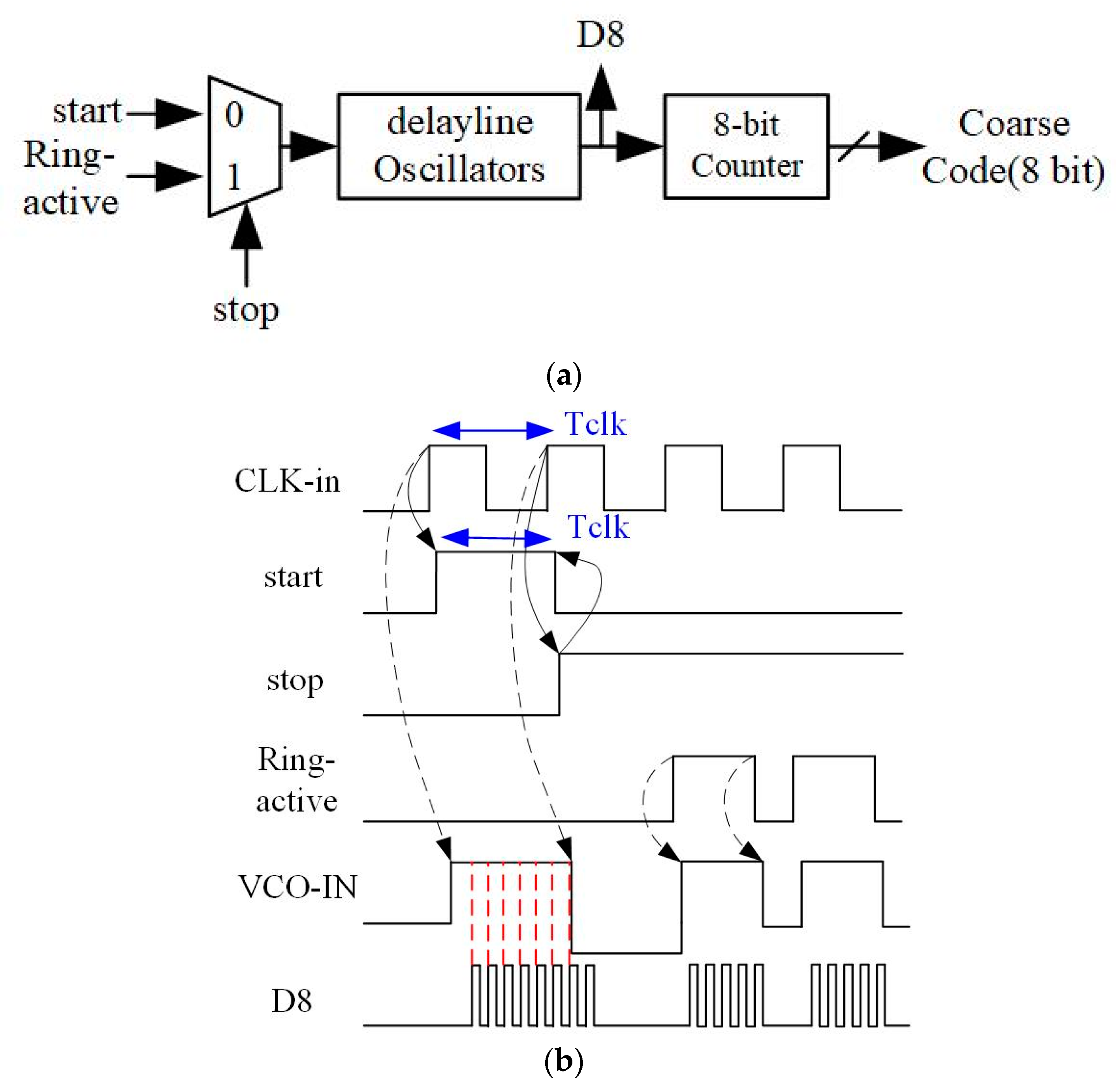
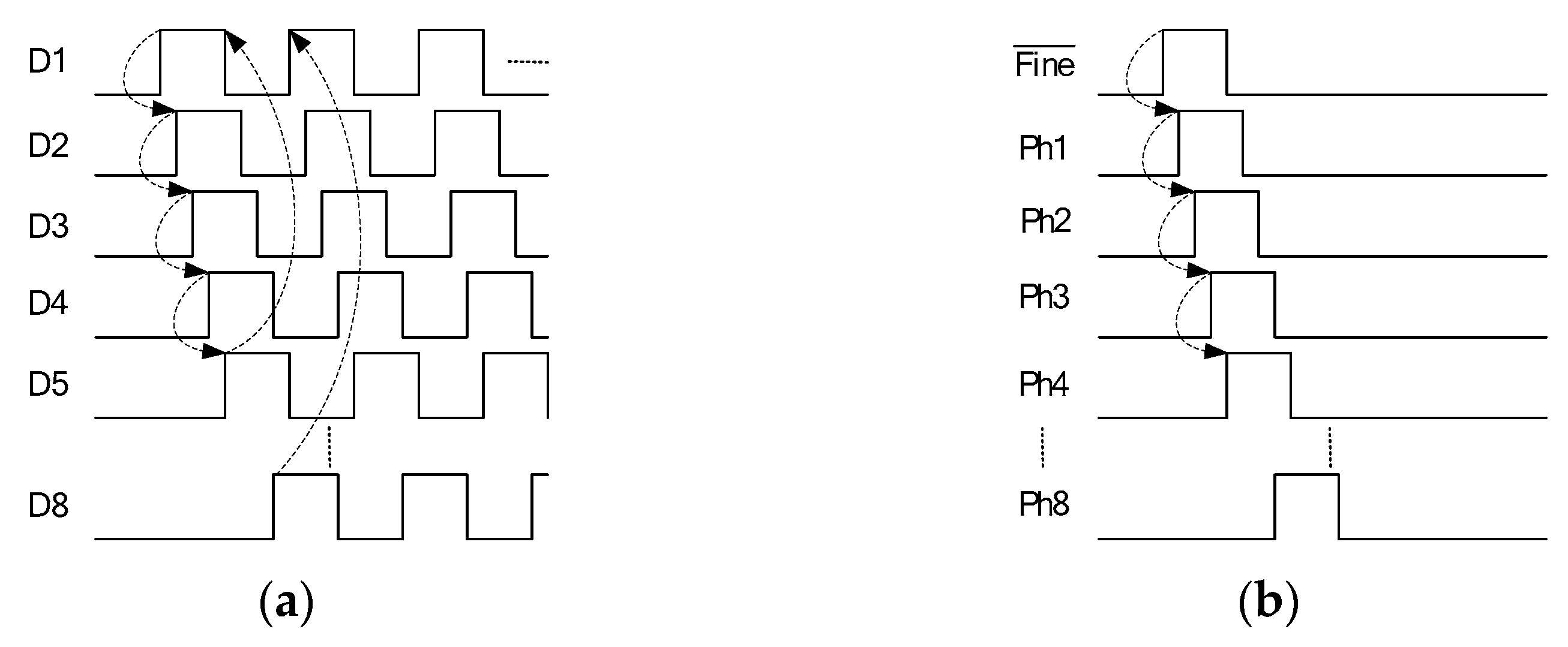
2.1. TDC
2.1.1. Fine TDC
2.1.2. Coarse TDC
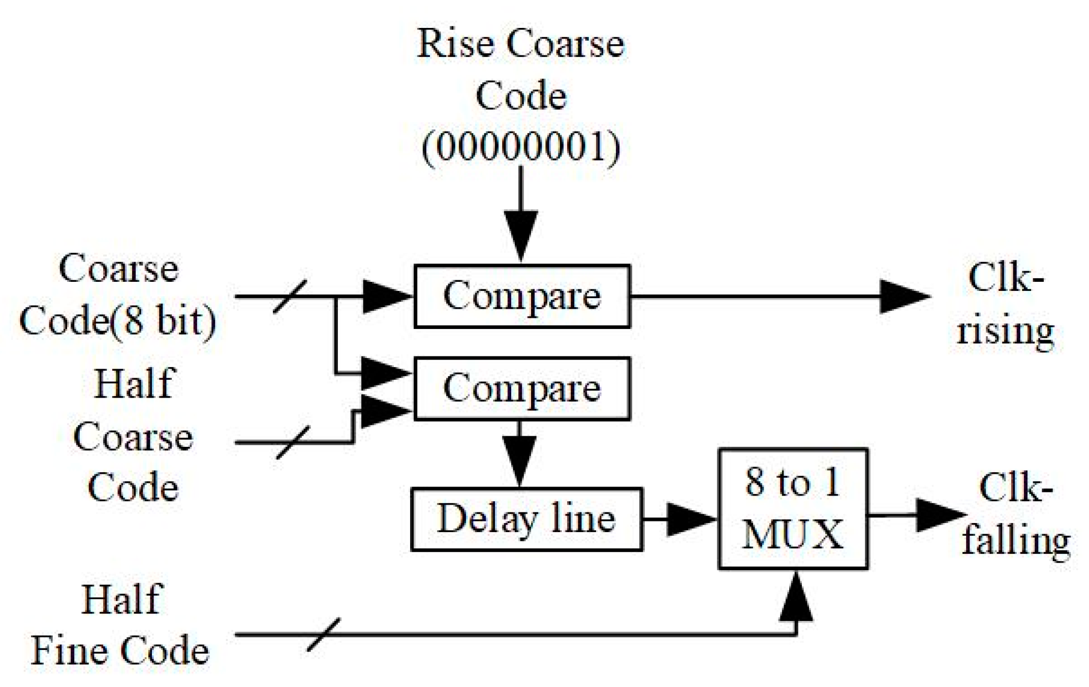
2.2. DTC
2.3. Ring-Active CKT
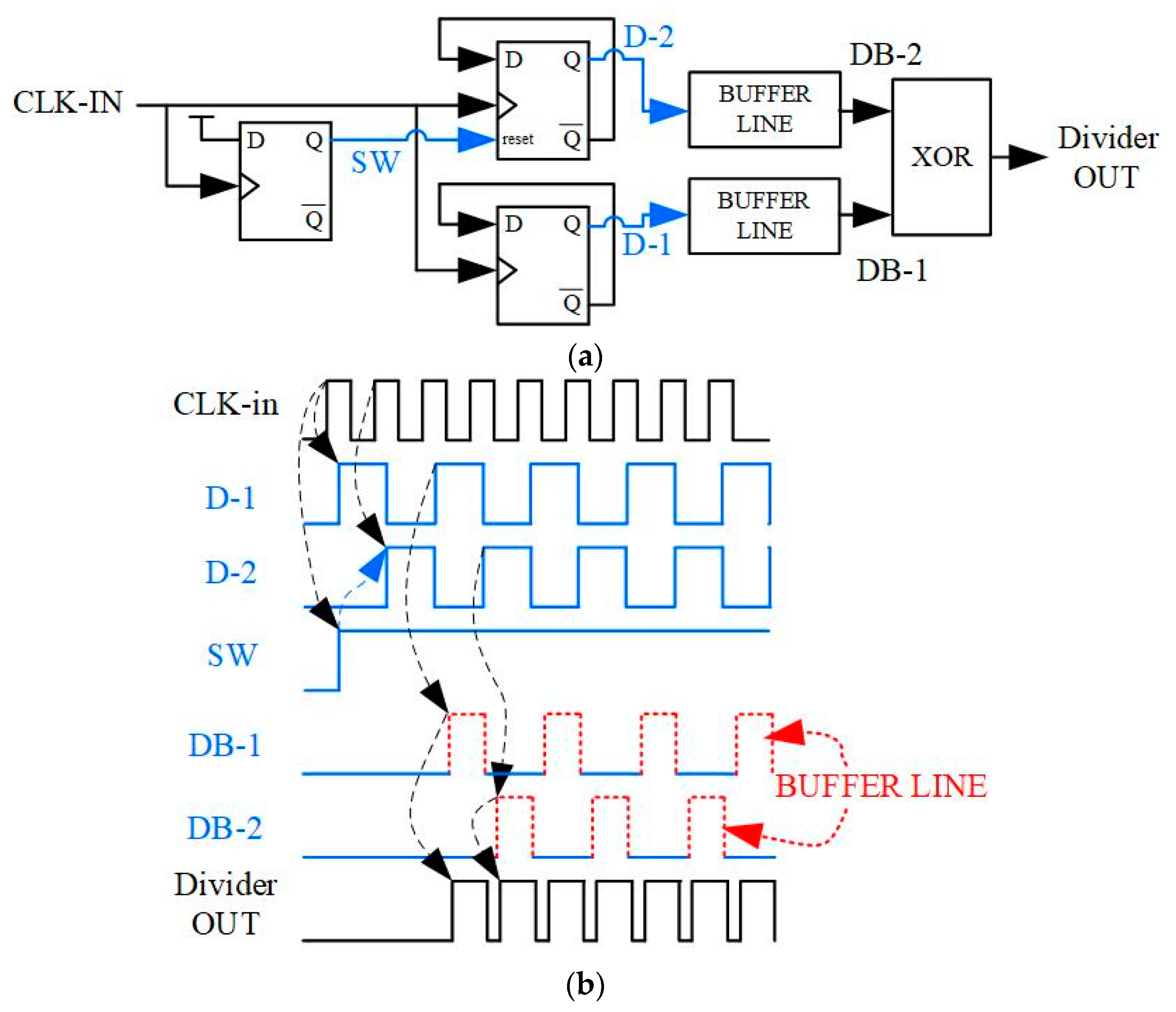
2.4. Delay Line Oscillators & Delay Line
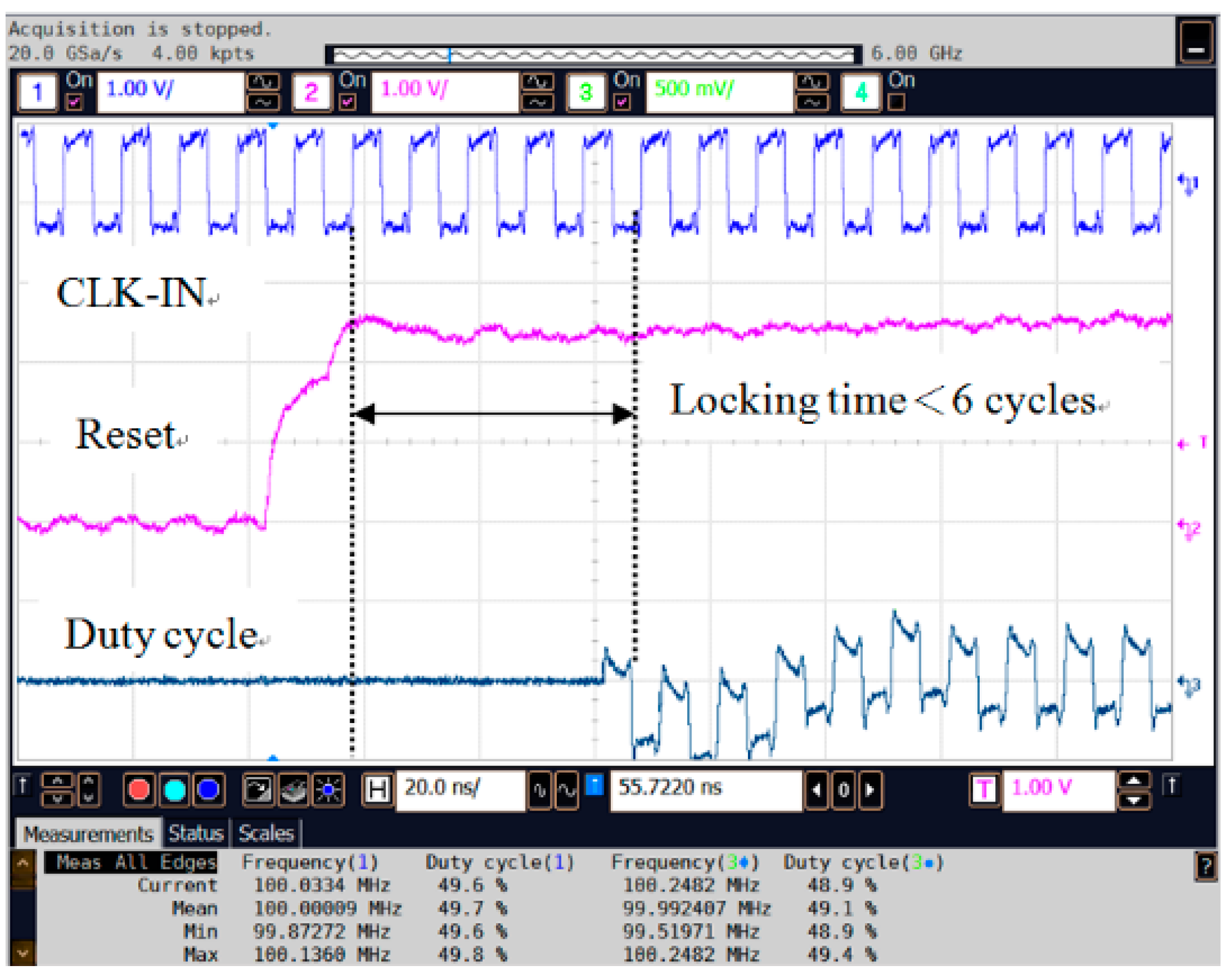
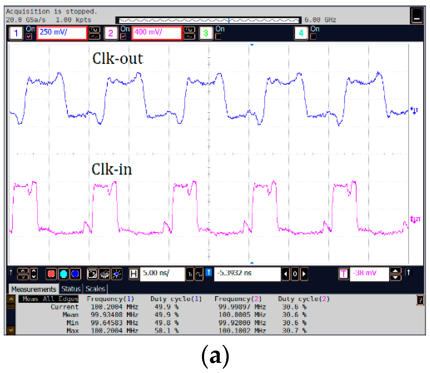
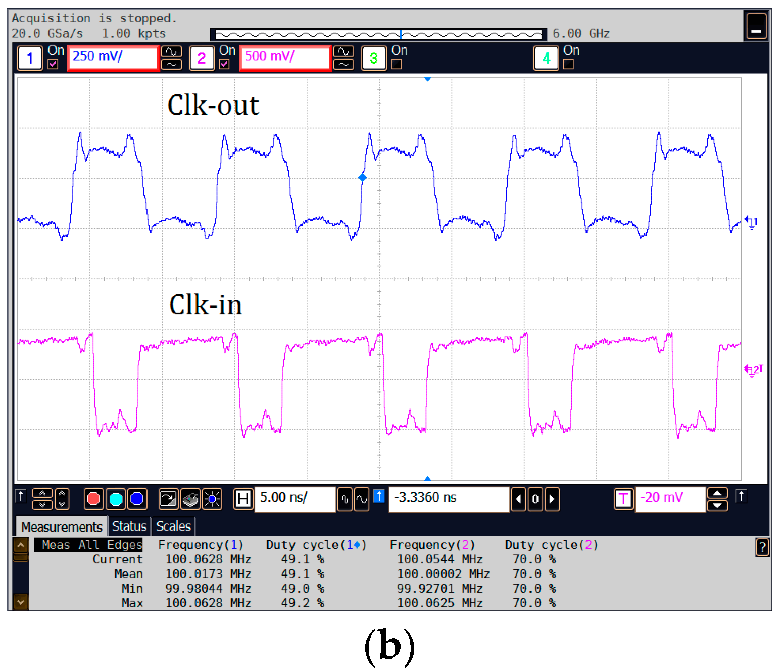
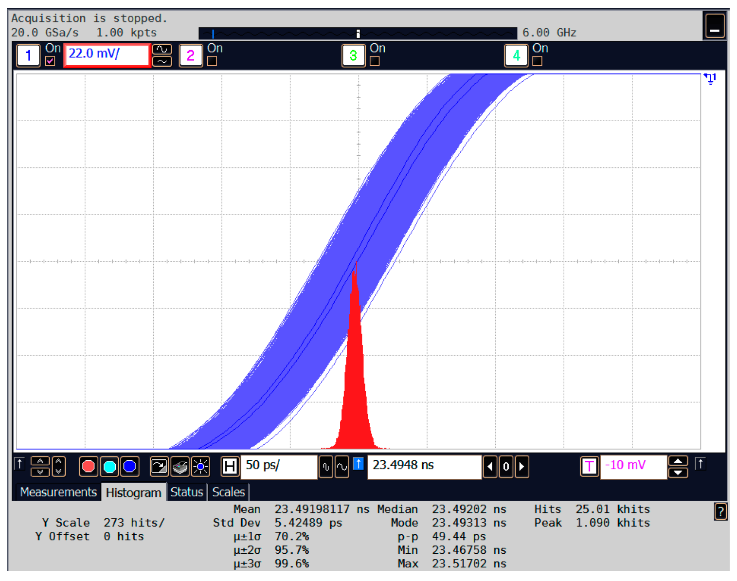
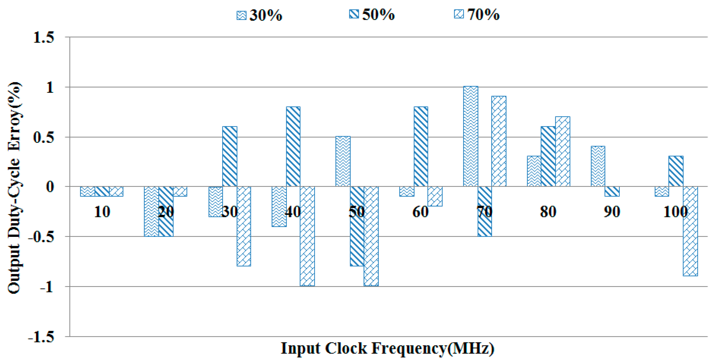
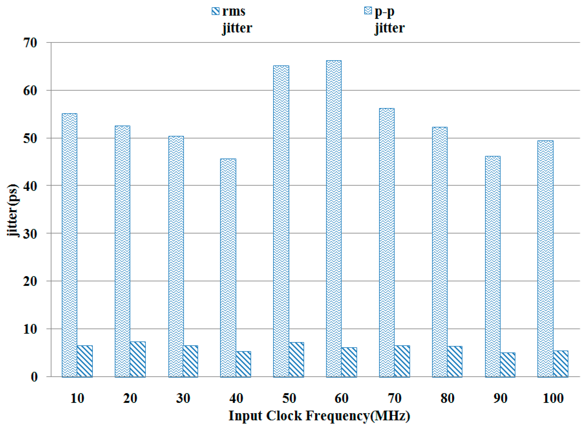
3. Experimental Results
4. Conclusions
Author Contributions
Funding
Institutional Review Board Statement
Informed Consent Statement
Data Availability Statement
Acknowledgments
Conflicts of Interest
References
- Lee, J.; Kim, B. A low-noise fast-lock phase-locked loop with adaptive bandwidth control. IEEE J. Solid-State Circuits 2000, 35, 1137–1145. [Google Scholar]
- Chiu, W.; Huang, Y.; Lin, T. A dynamic phase error compensation technique for fast-locking phase-locked loops. IEEE J. Solid-State Circuits 2010, 45, 1137–1149. [Google Scholar] [CrossRef]
- Hangmann, C.; Hedayat, C.; Hilleringmann, U. Stability analysis of a charge pump phase-locked loop using autonomous difference equations. IEEE Tran. Circuits Syst. I Regul. Pap. 2014, 61, 2569–2577. [Google Scholar] [CrossRef]
- Liang, C.; Yang, R.; Liu, S. An all-digital fast-locking programmable DLL-based clock generator. IEEE Tran. Circuits Syst. I Regul. Pap. 2008, 55, 361–369. [Google Scholar] [CrossRef]
- Yao, C.; Ho, Y.; Chiu, Y.; Yang, R. Designing a SAR-Based All-Digital Delay-Locked Loop With Constant Acquisition Cycles Using a Resettable Delay Line. IEEE Trans. Very Large Scale Integr. (VLSI) Syst. 2015, 23, 567–574. [Google Scholar] [CrossRef]
- Lin, W.M.; Huang, H.Y. A Low-Jitter Mutual-Correlated Pulsewidth Control Loop Circuit. IEEE J. Solid-State Circuits 2004, 39, 1366–1369. [Google Scholar]
- Wang, Y.J.; Kao, S.K.; Liu, S.I. All-Digital Delay-Locked Loop/Pulsewidth-Control Loop with Adjustable Duty Cycles. IEEE J. Solid-State Circuits 2006, 41, 1262–1274. [Google Scholar] [CrossRef]
- Nakamura, K.; Fukaishi, M.; Hirota, Y.; Nakamura, Y.; Yotsuyanagi, M. A CMOS 50% duty cycle repeater using complementary phase blending. In Proceedings of the IEEE International VLSI Circuits, Honolulu, HI, USA, 15–17 June 2000; pp. 48–49. [Google Scholar]
- Wang, J.; Wang, Y. An All-digital 50% duty-cycle corrector. In Proceedings of the IEEE International Circuits and Systems, Vancouver, BC, Canada, 2 May 2004; pp. 925–928. [Google Scholar]
- Yoo, C.; Jeong, C.; Kih, J. Open-loop full-digital duty cycle correction circuit. IET J. Electron. Lett. 2005, 41, 635–636. [Google Scholar] [CrossRef] [Green Version]
- Ogawa, T.; Taniguchi, K. A 50% duty-cycle corrector circuit for PLL output. Electron. Commun. Jpn. 2003, 86, 21–24. [Google Scholar]
- Shin, D.; Song, J.; Chae, H.; Kim, C. A 7 ps jitter 0.053 mm2 fast lock all-digital dll with a wide range and high resolution DCC. IEEE J. Solid-State Circuits 2009, 44, 2437–2451. [Google Scholar] [CrossRef]
- Chung, C.; Sheng, D.; Li, C. A Wide-Range Low-Cost All-Digital Duty-Cycle Corrector. IEEE Trans. Very Large Scale Integr. (VLSI) Syst. 2015, 23, 2487–2496. [Google Scholar] [CrossRef]
- Jeong, C.; Abdullah, A.; Min, Y.; Hwang, I.; Kim, S. All-digital duty-cycle corrector with a wide duty correction range for dram applications. IEEE Tran. Large Scale Integr. (VLSI) Syst. 2016, 24, 363–367. [Google Scholar] [CrossRef]
- Mohan, S.; Chan, S.; Colleran, M.; Greenwood, F.; Gamble, E.; Kouznetsov, G. Differential Ring Oscillators with Multipath Delay Stages. In Proceedings of the IEEE International Custom Integrated Circuits Conference, San Jose, CA, USA, 21 September 2005; pp. 635–638. [Google Scholar]


| [10] | [11] | [12] | This Work | |
|---|---|---|---|---|
| Type | Digital | Digital | Digital | Digital |
| Process (μm) | 0.35 | 0.25 | 0.35 | 0.35 |
| Supply Voltage (V) | 2.5 V | NA | 3.3 V | 3.3 V |
| Frequency range (MHz) | 250–600 | 400 | 400–600 | 10–100 |
| Duty cycle range | 40–60% | 2–98% | 30– 70% | 30– 70% |
| Total locked time | <5 cycle | <30 cycle | <28 cycle | ≤6 cycle |
| Duty cycle error | ±0.8% | −1.2–2.2% | ±0.6% | ±1% |
| Jitter (ps) | 64.4 ps @600 MHz | NA | 16.7 ps @500 MHz | 49.44 ps @100 MHz |
| Core size (mm2) | NA | NA | 0.68 | 0.27 |
Publisher’s Note: MDPI stays neutral with regard to jurisdictional claims in published maps and institutional affiliations. |
© 2021 by the author. Licensee MDPI, Basel, Switzerland. This article is an open access article distributed under the terms and conditions of the Creative Commons Attribution (CC BY) license (http://creativecommons.org/licenses/by/4.0/).
Share and Cite
Kao, S.-K. Design and Implementation of Fast Locking All-Digital Duty Cycle Corrector Circuit with Wide Range Input Frequency. Electronics 2021, 10, 71. https://doi.org/10.3390/electronics10010071
Kao S-K. Design and Implementation of Fast Locking All-Digital Duty Cycle Corrector Circuit with Wide Range Input Frequency. Electronics. 2021; 10(1):71. https://doi.org/10.3390/electronics10010071
Chicago/Turabian StyleKao, Shao-Ku. 2021. "Design and Implementation of Fast Locking All-Digital Duty Cycle Corrector Circuit with Wide Range Input Frequency" Electronics 10, no. 1: 71. https://doi.org/10.3390/electronics10010071