Article

Reliability and Economic Efficiency Analysis of 4-Leg Inverter Compared with 3-Leg Inverters

1
Department of Electronics and Control Engineering, Hanbat National University, Daejeon 34158, Korea
2
Department of Electrical Engineering, Chonnam National University, Gwangju 61186, Korea
3
Energy Conversion Research Centre, Korea Electronics Technology Institute, Gwangju 61011, Korea
*
Author to whom correspondence should be addressed.
Electronics 2021, 10(1), 87; https://doi.org/10.3390/electronics10010087
Submission received: 9 December 2020 / Revised: 29 December 2020 / Accepted: 30 December 2020 / Published: 4 January 2021
(This article belongs to the Section Power Electronics)

Abstract

:
The 4-leg inverter can adjust the load current or output voltage even under unbalanced load conditions, but it is known that the additional switch arm to the 3-leg inverter can increase the overall cost and the failure rate. This paper aims to analyze the failure rate and mean time between failures (MTBF) of 3-leg inverters and 4-leg inverters using part count failure analysis (PCA) and fault-tree analysis (FTA), and to compare the price of the inverters. The FTA can analyze the failure rate, including the type, number and connection status of the circuit components, and moreover the redundancy effect of the 4-leg inverter. For more accurate failure-rate prediction, the failure rate and MTBF of the 4-leg inverter according to the lifecycle of the controller are analyzed. Finally, by comparing the price of 3-leg inverters and 4-leg inverters using the cost model of major parts, the degree of reliability improvement against price increase is quantitatively analyzed.

1. Introduction

An inverter is a power converter that converts DC into AC, which allows simultaneous control of output voltage and frequency, and is used for various purposes such as motor drives based on VVVF (variable voltage and variable frequency) and grid-connection based on CVCF (constant voltage and constant frequency) control. Among the inverter circuit topologies, the three-phase 3-leg inverter is widely used as a power converter that connects distributed generation (DG) such as solar power, wind power or energy storage systems (ESS) to the grid [1,2,3,4,5]. However, if a DG network accident results in a current imbalance in the three-phase distribution network, the 3-leg inverter cannot supply an imbalanced current called a zero-sequence current. In this case, a 3-leg inverter employing a split DC-link capacitor or a 4-leg inverter can be a good alternative [6,7,8,9,10]. The 3-leg inverter with split DC-link capacitors works like that of three independent half-bridge inverters. Therefore, the line-to-neutral output voltage is half the input voltage, so the utilization of the input voltage becomes low, and moreover the DC-link capacitor directly handles the current flowing to the ground, so large capacitance is required [6,7]. The 4-leg inverter increases the switching loss by the added switch arm. Nevertheless, various modulation techniques are being studied because of the advantages of increasing DC-link voltage utilization [8,9,10] and the presence of 16 switching states, enabling output voltage adjustments for unbalanced loads and control of energy flow for each phase [11,12,13,14,15,16,17,18].
Three-dimensional space vector modulation (3D SVPWM), an extension of two-dimensional space vector modulation (2D SVPWM), was proposed, and 3D SVPWM was extensively studied [11,12,13,14,15]. A carrier-based PWM scheme using offset voltage has been proposed to alleviate the complexity of 3D SVPWM [16,17]. This research focuses only on the CPWM, which corresponds to class I of the 3D SVPWM, which has the effect of improving the THD but reduces the lifecycle of the inverter because each switch arm has a different power loss due to an unbalanced current. The above-mentioned 4-leg inverter modulation schemes commonly use 16 switching states appropriately to achieve various control objectives. In particular, the 4-leg inverter is capable of alternative operation even if a problem occurs with one switch arm of the 3-legs. In general, from a reliability perspective, increasing the number of parts increases the failure rate, but applying a control technique that takes into account the redundancy to a 4-leg inverter structure can lower the failure rate, which can predict the effect of improving reliability.
The reliability and economics of three-phase 3-leg and 4-leg inverters are analyzed in this paper by using the fault-tree analysis (FTA) technique, which can consider operational characteristics according to the redundancy characteristics of the 4-leg inverter. This study aims to accurately predict reliability according to the driving environment by analyzing the failure rate and MTBF (mean time between failures) by designing the fault-tree reflecting the operational risk according to the 3-leg and 4-leg inverter structure and control method. Among the various control methods for controlling the 4-leg inverter, the analysis is made by adding a redundancy function to the SVPWM method that can produce an increased output voltage compared with the sinusoidal PWM control method while keeping the switching frequency constant.
In this paper, we first define the failure of 3-leg and 4-leg inverters, and then design a fault-tree taking into account the operational characteristics. Second, using the fault library of MIL-HDBK-217F, we calculate the failure rate and the MTBF from the fault-trees. Third, we assume the lifecycle of the controller is 3 to 20 years and reflect this in the fault-tree to analyze the correlation between the lifecycle of the controller and the failure rate of the inverter. Fourth, we calculate the failure rate according to the part count failure analysis (PCA) method and compare it with FTA (fault-tree analysis) results to compare the advantages and disadvantages of 3-leg and 4-leg inverters in terms of reliability. Finally, through the economic analysis of 3-leg and 4-leg inverters, the overall cost is compared to the effect of reliability improvement.

2. Three-Phase 3-Leg and 4-Leg Inverter
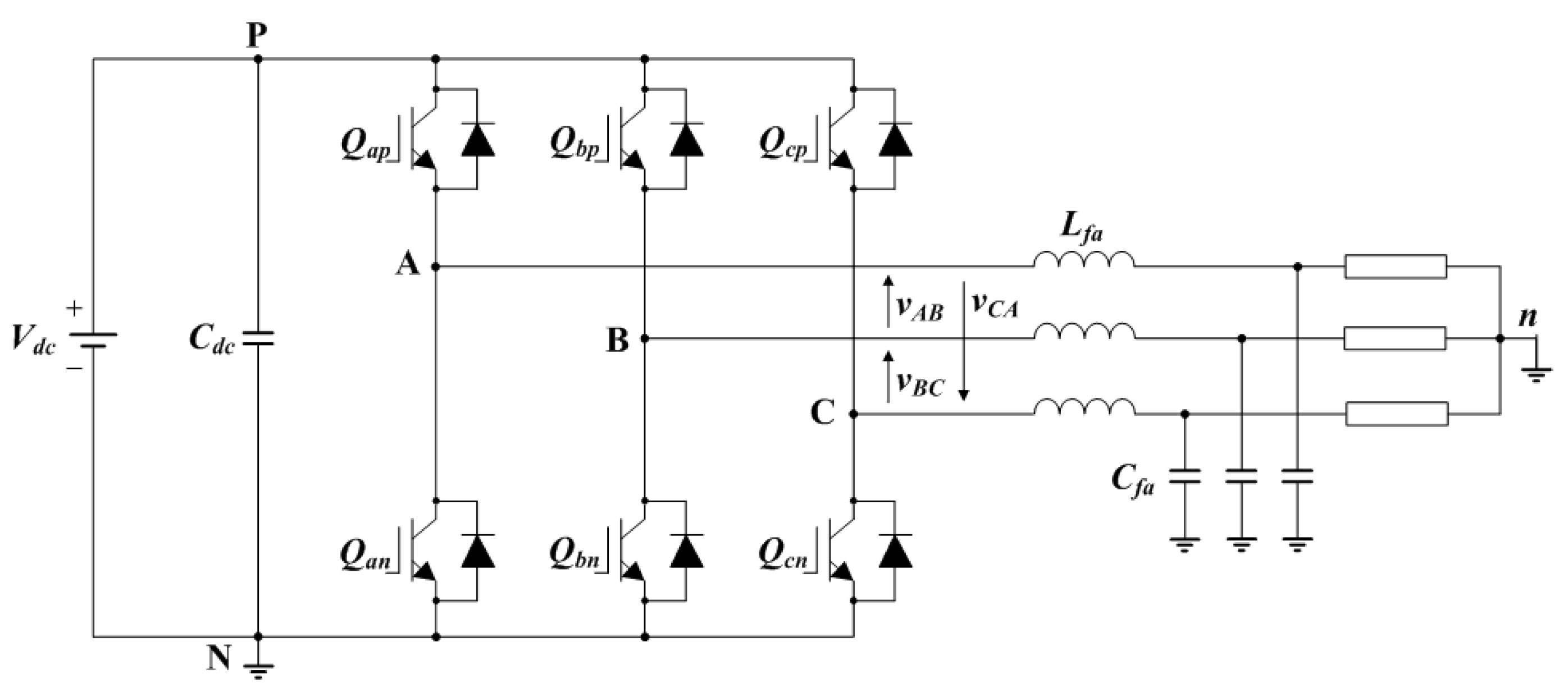
2.1. 3-Leg Inverter

The three-phase inverter generates a three-phase AC output voltage using a DC input source to supply power to the three-phase load. Figure 1 shows the circuit configuration of a three-phase 3-leg inverter. The 3-leg inverter consists of three switch arms that can operate independently of each other, and each arm produces its own arm voltage vA, vB, vC for three phases, where the reference for each arm voltage is determined as the potential of the N node corresponding to the (−) potential of the input voltage source. In this case, each arm voltage will be a momentary VDC or zero potential. The line-to-line voltage supplied to the load is vAB = vAvB, vBC = vBvC, vCA = vCvA, so the arm voltage is one of the two values of {VDC, 0} and the three-phase line voltage is one of the three values of {VDC, 0, −VDC}.
If the three-phase load is balanced, the phase voltage of the load has VDC or 0, and each phase of the load is connected to either of these two voltages. Therefore, if one switch arm fails, an imbalance of power supplied to the three-phase load is inevitable.

2.2. 3-Leg Inverter Employing Split DC-Link Capacitor
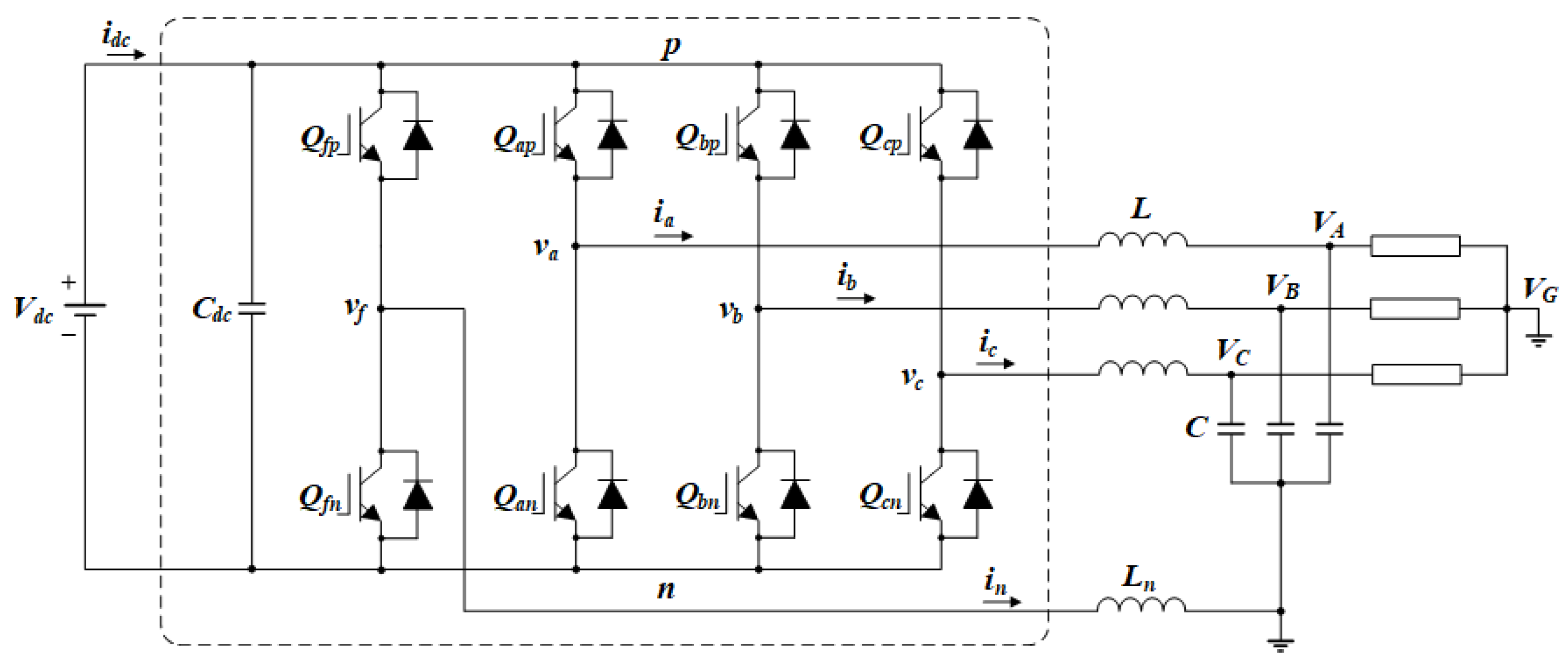
To compensate for these unbalanced problems, a 3-leg inverter circuitry with split DC-link capacitors can be used as shown in Figure 2. A three-phase 3-leg inverter with split DC-link capacitors consists of three switch arms that can operate independently of each other and each arm produces its own arm voltage vA, vB, vC for three phases. Here the reference potential for each arm voltage is determined by the neutral point of the series-connected capacitor. In this case, each arm voltage will be a momentary VDC/2 or −VDC/2. The line-to-line voltage supplied to the load is vAB = vAvB, vBC = vBvC, vCA = vCvA, so the arm voltage is one of the two values of {VDC/2, −VDC/2} and the three-phase line voltage is one of the three values of {VDC, 0, −VDC}.
In Figure 2, the neutral point current flows through the DC-link capacitor, and the ground is clamped by half the DC-link voltage. The 3-leg inverter with split DC-link capacitors is the same as the three half-bridge inverters being driven independently. Therefore, the line-to-neutral output voltage is half the input voltage, so the utilization of the input voltage source is low, and moreover the DC-link capacitor directly handles the current flowing to the ground, so the capacitance increases unrealistically. In conclusion, it is possible to supplement the load imbalance problem, but in the case of a switch arm failure, it is impossible to operate an alternative operation to secure redundancy.

2.3. 4-Leg Inverter

Figure 3 shows the circuit configuration of the 4-leg inverter. The additional switch arm controls the neutral voltage and the neutral current. This allows the 4-leg inverter to generate three independent output voltages regardless of load conditions. In other words, even if one switch arm fails, it is possible to secure 100% redundancy that allows alternative switching operation.

3. Reliability Analysis of Inverters

To compare the reliability of 3-leg and 4-leg inverters, this chapter calculates the failure rate and MTBF (mean time between failures) through part count failure analysis (PCA) and fault-tree analysis (FTA) under conditions where the inverters are controlled by the SVPWM. Figure 4 shows the power stage of the 4-leg inverter and the controller based on TMS320F2835. Table 1 represents the specification of the 4-leg inverter and the 3-leg inverter is constructed using the same component. The types and number of parts that make up the inverter and controller vary widely. Reliability and economics are analyzed for relatively expensive parts, such as the main components IGBT (Insulated Gate Bipolar Transistor), capacitors and inductors, because it is difficult to consider all components in reality. For capacitors, we analyze the electrolytic capacitor of DC-link and the film capacitor for filtering purpose. Supercapacitor can also be analyzed as important parts of the inverter depending on its application area [19], but it is excluded because it is difficult to analyze accurately due to a lack of experimental data.

3.1. Calculation of Part Failure Rate by MIL-HDBK-217F

To calculate the failure rate of inverters using PCA and FTA, it is first necessary to calculate the failure rate of parts for the IGBT, the capacitor the and inductor, which are the main circuit components that consist of the inverter. In this paper, we use the fault library of MIL-HDBK-217F, which provides a failure-rate calculation equation for each part [20,21]. It considers various factors such as basic failure rate, power capacity, voltage rating, application, temperature, environment, quality factor, etc. The experimental Equations (1)–(6) are the result of reflecting the specification given in Table 1 for MIL-HDBK-217F’s failure-rate calculation formula; the quality factor is based on the commercial product and the environment factor is based on the state in which the inverter is a controlled environment.

3.1.1. Failure Rate of IGBT

The MIL-HDBK-217F does not provide failure rates for IGBTs. Since IGBT consists of series combinations of BJT and MOSFET equivalent, failure of either will result in failure of IGBT. Therefore, the failure rate of IGBT is calculated through the OR-gate operation of the two elements [22].
λ IGBT = 1 ( 1 λ BJT ) ( 1 λ MOSFET )   failures / 10 6 h
λ BJT = 0 . 00076923 ( P r ) 0.37 exp ( V C E _ a p p l i e d V C E O _ r a t e d ) exp [ 2114 ( 1 T J + 273 1 298 ) ]   failures / 10 6 h
λ MOSFET = 3.96 exp [ 1925 ( 1 T J + 273 1 298 ) ]   failures / 10 6 h
where (2) and (3) are the failure rate based on the experimental data of BJT and MOSFET, respectively. Here, TJ is the junction temperature (°C), Pr is the rated power (W), VCE-applied is the collector–emitter applied voltage, VCEO-rated is the collector–emitter rated voltage in the base open state.

3.1.2. Failure Rate of DC-Link Capacitor

The failure rates of electrolytic capacitors (aluminum oxide) used as DC-link capacitors are given in (4).
λ C _ d c = 0 . 012 ( C ) 0.23 [ ( V o p e r a t i n g 0.6 V r a t e d ) 5 + 1 ] exp [ 0.35 8.617 × 10 5 ( 1 T + 273 1 298 ) ]   failures / 10 6 h
Equation (4) is the failure rate based on the experimental data of an electrolytic capacitor. Here, C is the capacitance (μF) of the capacitor. Voperating is the working voltage of the capacitor, the sum of the DC voltage and AC voltage peak applied to the capacitor, and Vrated is the rated voltage of the capacitor. T is the ambient temperature (°C) of the capacitor.

3.1.3. Failure Rate of Filter Capacitor

The metalized polypropylene film capacitor is employed as an AC filter capacitor, and the failure rate according to the experimental data is shown in (5).
λ C _ f = 0 . 051 ( C ) 0.09 [ ( V o p e r a t i n g 0.6 V r a t e d ) 5 + 1 ] exp [ 0.15 8.617 × 10 5 ( 1 T + 273 1 298 ) ]   failures / 10 6 h
Equation (5) is the failure rate based on the experimental data of the metalized polypropylene film capacitor. Here, C is the capacitance (μF) of the capacitor. Voperating is the working voltage of the capacitor, the sum of the DC voltage and AC voltage peak applied to the capacitor, and Vrated is the rated voltage of the capacitor. T is the ambient temperature (°C) of the capacitor.

3.1.4. Failure Rate of Filter Inductor

The failure rate of the AC filter inductor according to experimental data is given in (6).
λ L = 0 . 00054 exp [ 0.11 8.617 × 10 5 ( 1 T H S + 273 1 298 ) ]   failures / 10 6 h
T H S = T A + 1 . 1 ( Δ T )
Here, the hot spot temperature of the inductor THS (°C) is calculated by (7). TA is the ambient temperature (°C) at which the inductor operates and ΔT is the average temperature rise above the ambient temperature (°C).

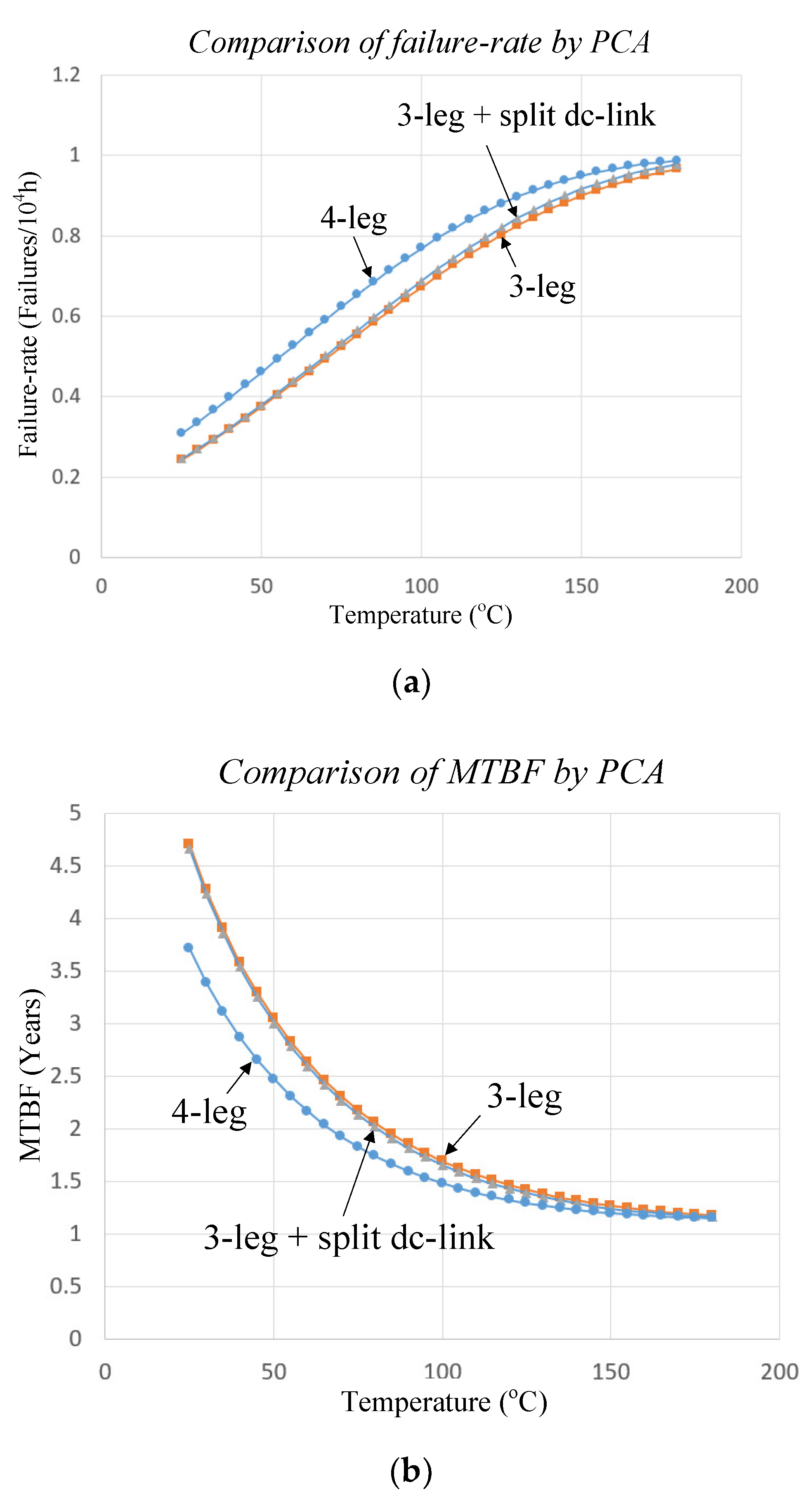
3.2. Failure Rate by Part Count Failure Analysis (PCA)

Figure 5 shows the failure dependence of a 3-leg inverter in application to PCA. Failure of 3-leg inverter is caused by failure of six IGBTs, a DC-link capacitor, three AC filter capacitors, three AC filter inductors and output load failure. If any of the components fails, it has an OR-gate dependency that leads to a failure of the 3-leg inverter. We calculate the failure rate of the 3-leg inverter by substituting the part failure rate calculated as MIL-HDBK-217F for the failure dependence shown in Figure 5. Here, the output load failure rate reflects 1% of AC filter inductor with the lowest failure rate among key components to minimize the impact on the inverter failure rate under analysis and to reflect some portions of the effect of temperature rise [23,24,25].
Figure 6 shows the failure dependence of a 3-leg inverter with split DC-link capacitors. Failure of the inverter is caused by failure of six IGBTs, two DC-link capacitors, three AC filter capacitors, three AC filter inductors and output load failure. If any of the components fails, it has an OR-gate dependency that leads to a failure of the inverter.
Figure 7 shows the failure dependence of a 4-leg inverter. Failure of 4-leg inverter is caused by failure of eight IGBTs, a DC-link capacitor, three AC filter capacitors, three AC filter inductors, a neutral inductor and output load failure. If any of the components fails, it has an OR-gate dependency that leads to a failure of the 4-leg inverter. It is a configuration in which two IGBTs and one neutral inductor are added compared to a 3-leg inverter.
Figure 8a shows a comparison of the failure rate of the three-phase inverters by the PCA method. The 4-leg inverter has the highest failure rate at 25~180 °C. At 25 °C, the failure rate of the 3-leg inverter is 0.243 failures/104h, and the Split DC-link capacitor 3-leg inverter shows 0.245 failures/104h, but the 4-leg inverter represents a relatively high failure rate of 0.307 failures/104h. The increased failure rate of approximately 0.065 failures/104h compared to 3-leg inverters is the result of an increase of two IGBTs. The difference in failure rates is reduced by 32% at 180 °C to approximately 0.021 failures/104h.
Figure 8b shows the MTBF of a 3-leg inverter at 25 °C is 4.7 years, the split DC-link capacitor 3-leg inverter is 4.66 years, but the 4-leg inverter represents a relatively small MTBF of 3.71 years. The difference in MTBF is about 0.99 years at 25 °C and decreases to about 0.025 years at 180 °C. The reason why the difference in failure rates decreases as the temperature increases is that at higher driving temperatures, the effect of increasing failure rates by temperature is greater than that by the number of parts.

3.3. Failure Rate by Fault-Tree Analysis (FTA)

This chapter designs and analyzes fault-trees for reliability analysis considering the operational characteristics of 3-leg inverters and 4-leg inverters. The design of a fault-tree requires an analysis of the various causes and consequences of failure of the inverter [26,27,28]. The causes of failure and the effects of the failure are very complex, so it is very difficult to consider all conditions. Therefore, we design a fault-tree for major failures with high RPN (Risk Priority Number) values defined by the multiplication of severity, frequency of occurrence and detectability of failures in FMECA (Failure Mode, Effects Analysis and Criticality Analysis) [29,30].
Fault-Tree Analysis (FTA) is a quantitative failure analysis method that logically analyzes the cause of failures and makes a fault-tree and uses it to obtain the probability of failure. The FTA is a top-down approach that uses Boolean algebra (AND, OR-gate, etc.) in graphical representations to express logical inter-relationships between basic and top events.

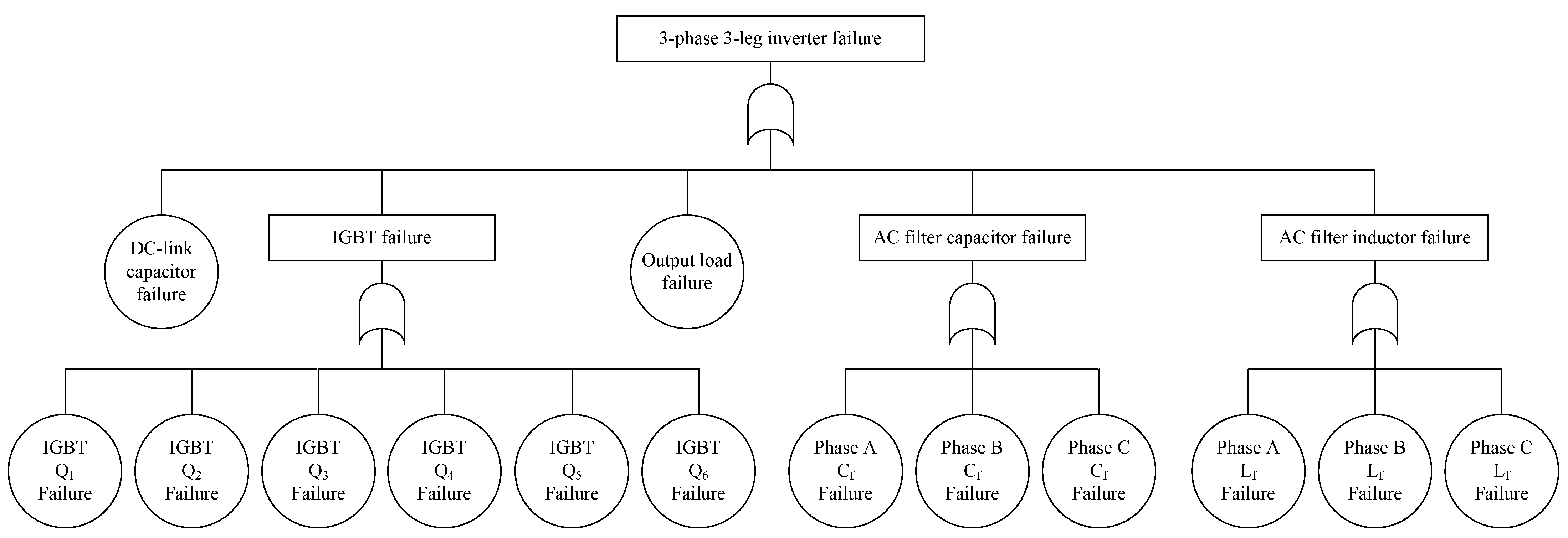
3.3.1. Fault-Tree Design of 3-Leg Inverter

Figure 9 shows the fault-tree of a three-phase 3-leg inverter. Failure of the 3-leg inverter is defined as failure of the output voltage generation function. Since the top-level failure of the 3-leg inverter is defined as a failure of the output voltage generation, the cause of the lower stage failure may be the failure of each phase voltage control. Function failures that control the amplitude and frequency of the output voltage are defined as failures on each phase, not separately classified. In addition, the input of the 3-leg inverter is assumed to be supplied by the DC-link capacitor, and the probability of failure of the front-end system supplying power to the DC-link capacitor is included in the DC-link capacitor failure. The main goal is to analyze the reliability of the 3-leg inverter itself. Therefore, the type and condition of the load are treated as a failure of Output load failure] without being specifically identified.
[DC-link power supply failure] consists of OR-gate combination of [DC-link capacitor intrinsic function failure] and [DC-link front-end circuit function failure]. The electrolytic capacitor, which is a DC-link capacitor, is responsible for charging and discharging functions for maintaining DC-link voltage, but may lose its original function due to short circuit, opening and failure of the capacitor itself. Therefore, sub-failures are designed with [Capacitor short failure], [Capacitor open failure] and [DC-link failure]. Since the input of the 3-leg inverter assumes that it is supplied by the DC-link capacitor, the probability of failure of the front-end system supplying power to the DC-link capacitor is included in the DC-link capacitor failure.
[IGBT switching function failure] occurs from the loss of switching function of the upper and lower IGBT of each arm. The causes of [Qxp switching function failure] can be seen as [IGBT intrinsic function failure] and [Switching signal generation failure]. [IGBT intrinsic function failure] is caused by short circuit, open circuit, overheating due to loss of heat-sink function and failure of IGBT itself. Therefore, the sub-event of [Qxp switching failure] is designed as an OR-gate combination of [IGBT Qxp failure], [Short circuit failure], [Open circuit failure] and [Heat-sink failure].
The causes of failure for generating a switching signal of [switching signal generation function failure] are control IC failure, failure of control algorithm and failure of gate-amp. Therefore, the sub-event of [Switching signal generation failure] is designed with OR-gate combination of [Gate-amp function failure], [Control signal generation failure] and [Control IC failure]. [Control signal generation failure] is due to a problem with the control algorithm itself or to failure of the feedback function due to failure of the PT, CT sensor, etc. Therefore, the sub-event of [Control signal generation failure] is designed as an OR-gate combination of [Control Algorithm failure] and [Feedback function failure].
[AC filtering function failure] consists of the OR-gate combination of [AC filter Lfx failure] and [ac filter Cfx failure]. The inductor and capacitor located at the output stage of each phase are responsible for generating high quality output voltage by LC filtering the inverter output voltage. While there are many possible causes of failure, only the inductor and capacitor itself are considered as they have relatively low failures compared to IGBT, DC-link capacitors and others.

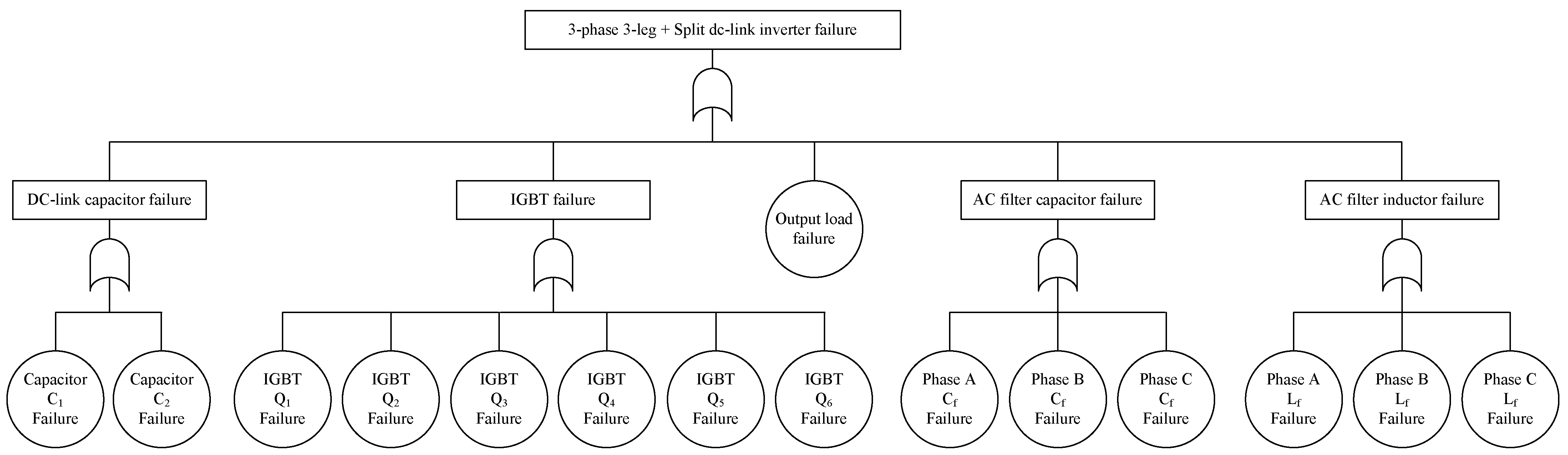
3.3.2. Fault-Tree Design of 3-Leg Inverter Employing Split DC-Link Capacitors

Figure 10 shows a fault-tree of three-phase 3-leg inverter employing split DC-link capacitors. Another DC-link capacitor is added compared to the 3-leg inverter in Figure 9, adding a red dotted box, an event indicating a failure of that function. This shows that each capacitor failure is designed to be reflected, taking into account the structure of the split DC-link capacitor. An increase in failure rate can be expected as much as an electrolytic capacitor, a DC-link capacitor, compared with the failure rate of a 3-leg inverter.

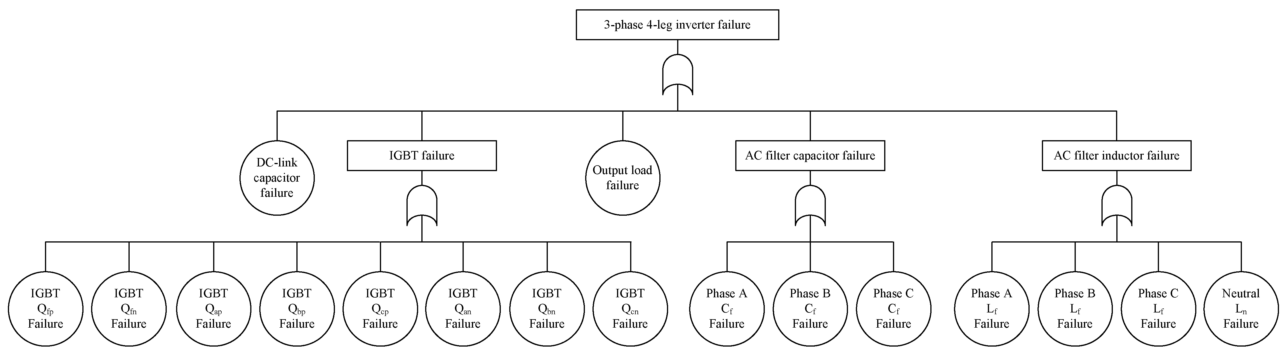
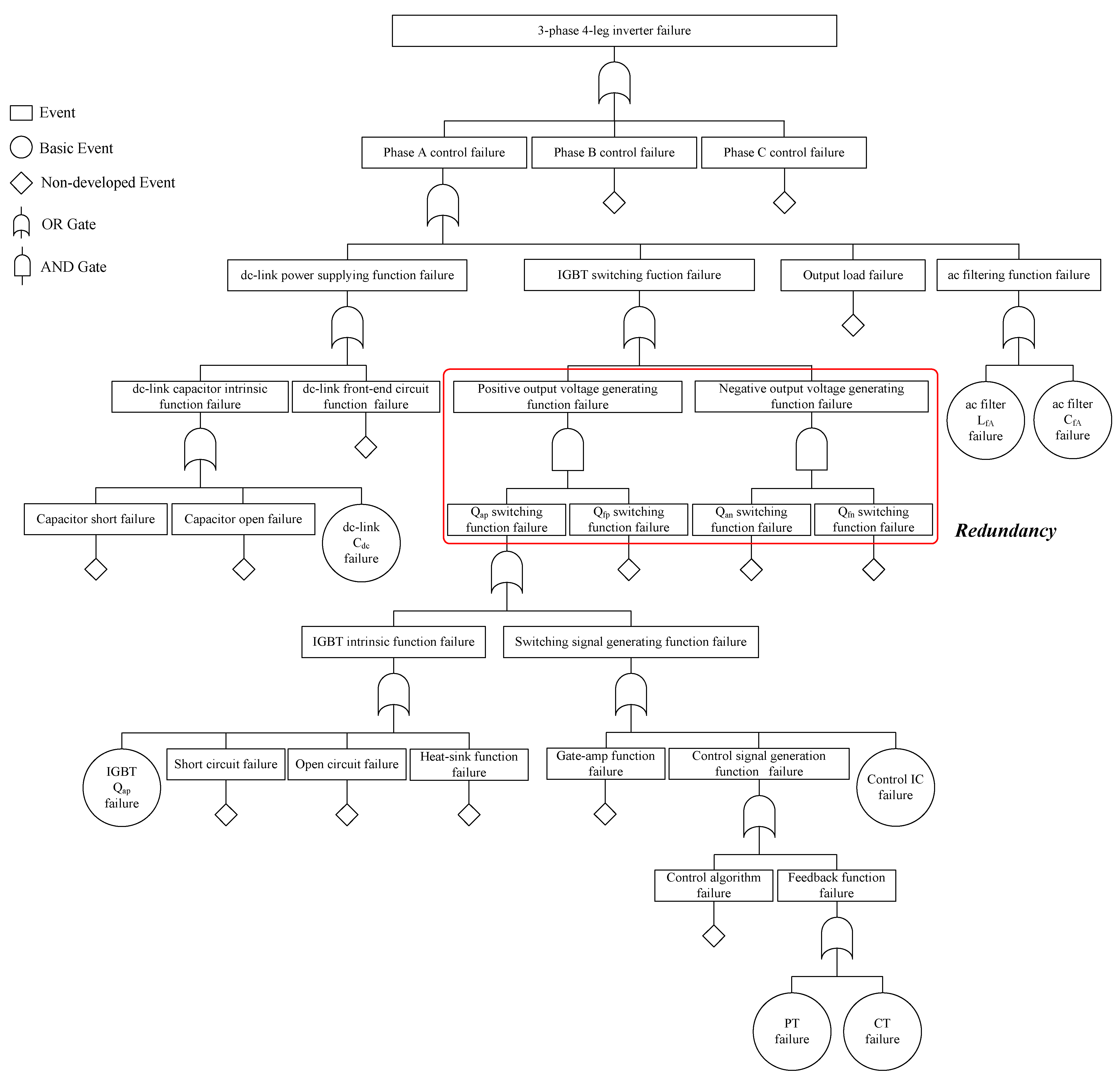
3.3.3. Fault-Tree Design of 4-Leg Inverter

Figure 11 shows the fault-tree of a 4-leg inverter. Failure of the 4-leg inverter is defined as failure of the output voltage generation function like that of 3-leg inverter. The red dotted box represents an [IGBT switching function failure] event, which differs from the 3-leg inverter in the fault-tree of a 4-leg inverter. The 4-leg inverter is a structure in which one switch arm is added to the 3-leg inverter. Thus, even if a failure of the IGBT responsible for each phase occurs, the output compensation of the load phase voltage can be achieved through the alternate switching control of the added switch. If the 4-leg inverter meets the 100% redundancy condition, the added switch arm operates completely separate for positive (+) and negative (−) output phase voltage, so the sub-event of [IGBT switching function failure] is designed with OR-gate combination. [Positive (or negative) output voltage generation failure] is designed as AND-gate combination of [Qap (or Qan) switching function failure] and [Qfp (or Qfn) switching function failure] taking into account 100% redundancy condition.
Figure 12 shows the phase current (ia, ib, ic) and neutral point current (in) of the 4-leg inverter. Figure 12a shows each phase current waveform in a balanced three-phase load. It has the same amplitude of the phase current and a neutral current is zero. Figure 12b shows the phase current when the load of phase A is half of the phase B and C loads by load imbalance. The load is balanced by allowing the phase current as much as the reduction of phase A current (ia) to flow over the additional switch arm. Figure 12c shows the load phase current and neutral current (in) when the load of phase C doubles the load of phases A and B due to load imbalance. When the amplitude of the phase C current (ic) is greater than the current amplitude for the other two phases (ia, ib), the neutral current (in) appears to be the same amplitude as the A and B phases but with phase differences. Figure 12d shows a condition in which the phase C current (ic) cannot flow due to a fault in phase C. The 4-leg inverter, which has the redundancy characteristic, is kept in a balanced three-phase through alternative operation of the additional switch arm.
Figure 13a shows a comparison of the failure rate of the three-phase inverters by FTA. The 4-leg inverter has the lowest failure rate, in the range of 25 to 180 °C. At 25 °C, the 3-leg inverter exhibits 0.247 failures/104h, and the split DC-link capacitor 3-leg inverter exhibits 0.254 failures/104h, similar to the failure rate results for PCA. However, for 4-leg inverters, the PCA has a failure rate of 0.307 failures/104h, but the FTA has a very low failure rate of 0.0266 failures/104h. This is because the PCA only considers the type, number and connection of components, but the FTA also considers the operating characteristics of inverters. The 4-leg inverter is a structure in which two IGBT switches with relatively high failure rates are added, but in substance it shows that the added switch arm allows redundancy for each output phase voltage generation, which can significantly reduce the failure rate.
The MTBF in Figure 13b shows that the 3-leg inverter at 25 °C is 4.6 years and the split DC-link capacitor 3-leg inverter is 4.5 years, similar to the results for PCA, but the 4-leg inverter shows a significant increase in lifecycle to about 43 years. However, as the temperature increases, the difference in failure rates decreases compared to PCA results because at higher driving temperatures the effect of increasing failure rates due to temperature is greater than that due to the operating characteristics of the inverter.

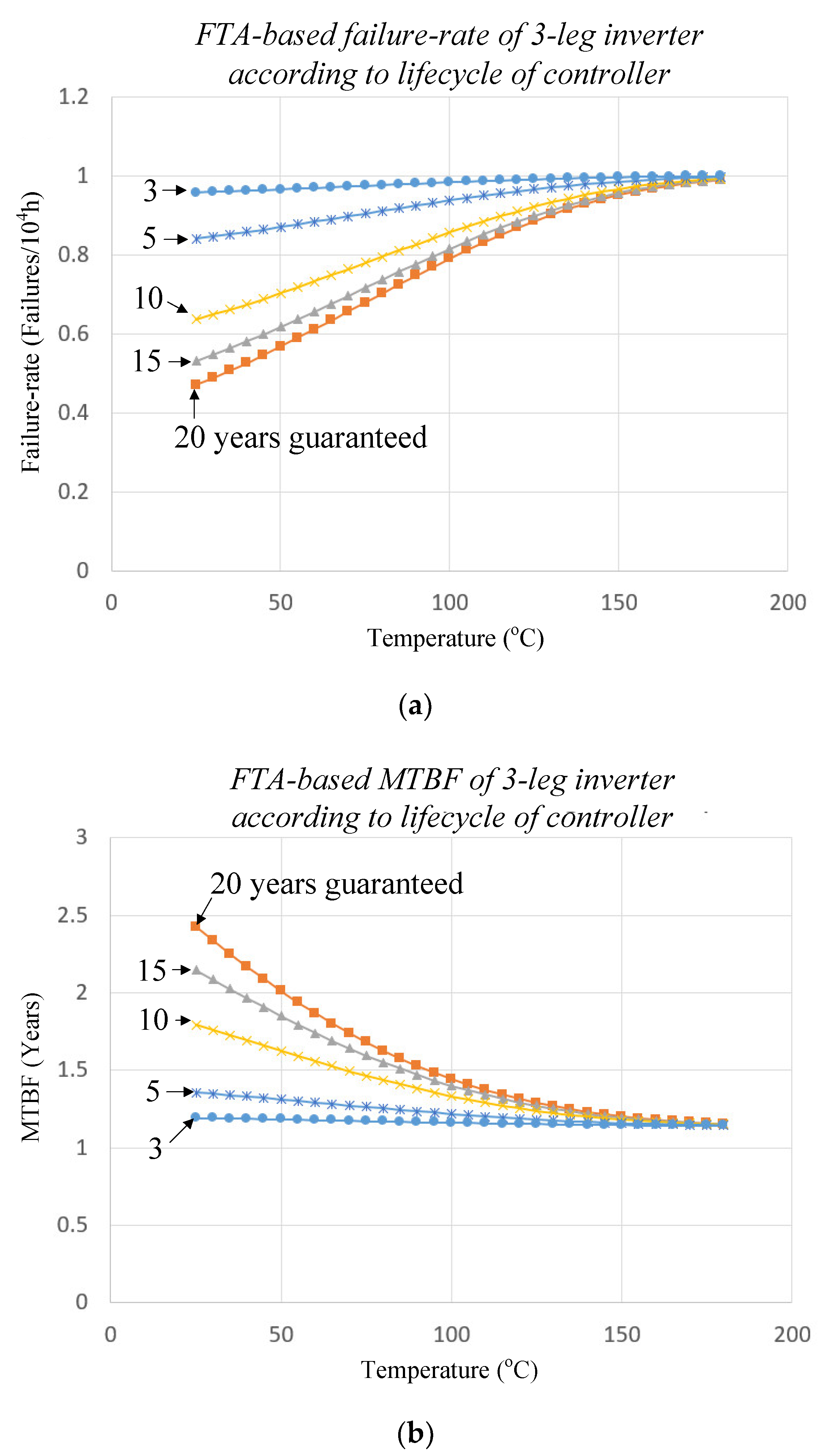
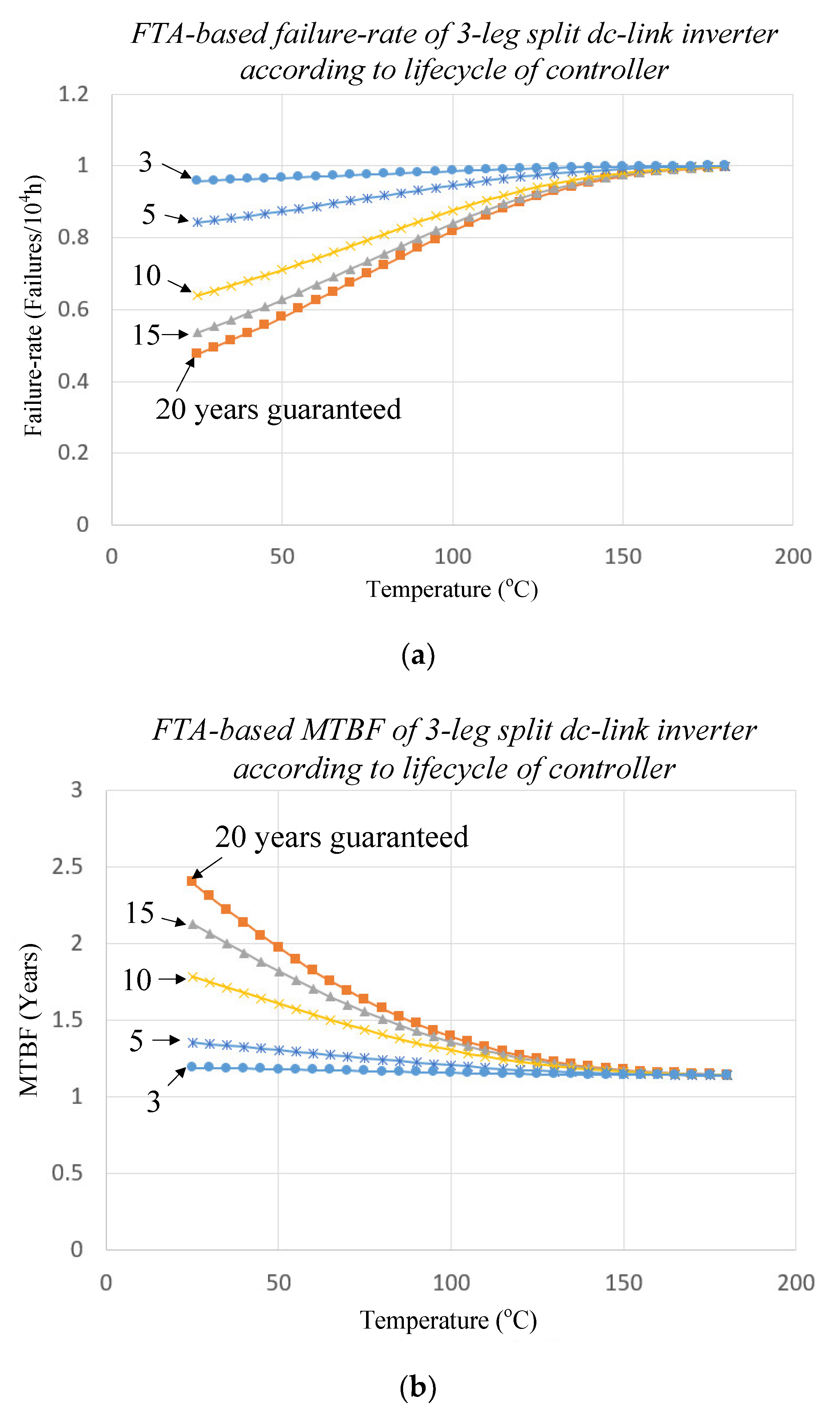
3.4. Failure Rate of the Three-Phase Inverter According to the Reliability of the Controller

This section analyzes the failure rate of the inverter according to the reliability of the controller applied to the three-phase inverter. The three-phase inverter can apply various control techniques, such as sinusoidal PWM, SVPWM, depending on the purpose of control. These control algorithms are implemented by control ICs, peripheral circuits, etc., and the severity of failure rates due to performance differences in the control algorithm itself is difficult to assess realistically. Even if performance or complexity between control techniques is considered, the degree of difference in failure rates is not significant and the impact on failure rate analysis is small. Thus, in this paper, the failure of a [Switching signal generation function failure] event corresponding to the controller function in the fault-tree is set to 3, 5, 10, 15 and 20 years and the inverter failure rate and MTBF are analyzed for the analysis of how much the controller including the control algorithm affects the overall reliability of the inverter. Table 2 shows the MTBF converted to failure rate (failures/104h).
Figure 14a shows the failure rate of the 3-leg inverter according to the lifecycle of the controller using the FTA. At 25 °C, it is analyzed as 0.47 failures/104h for 20 years, 0.53 failures/104h for 15 years, 0.64 failures/104h for 10 years, 0.84 failures/104h for five years and 0.96 failures/104h for three years of controller lifecycle. It shows that the MTBF of a controller decreases every five years; the failure rate increases almost twice as much. It should be noted that if the MTBF of the controller at 25 °C is less than five years the failure rate of the 3-leg inverter will increase rapidly to 0.84 failures/104h. In particular, if the MTBF of the controller is designed to be less than three years, the failure rate of a 3-leg inverter is higher than 0.96 failures/104h, indicating that the lifecycle of the controller is a condition that significantly affects the failure rate of the 3-leg inverter.
Figure 14b shows the MTBF of the 3-leg inverter according to the lifecycle of the controller. In order for a 3-leg inverter to obtain MTBF of more than two years at 25 °C, the MTBF of the controller must be guaranteed at least 15 years. In particular, it should be noted that the MTBF of a 3-leg inverter decreases sharply to 1.36 years, if the controller MTBF is less than five years at 25 °C. In operating conditions above 100 °C, it falls below 1.5 years regardless of the MTBF of the controller, as the failure rate increases due to the greater influence on the operating temperature than the lifecycle of the controller.
Figure 15a shows the failure rate of the split DC-link capacitor 3-leg inverter according to the lifecycle of the controller using the FTA. Similar to a 3-leg inverter, the five-year reduction in the controller’s MTBF shows that the failure rate almost doubles. If the MTBF of the controller is not more than five years under 25 °C operating conditions, it shall be noted that the failure rate of the split DC-link capacitor 3-leg inverter has increased rapidly to 0.84 failures/104h. In particular, if the MTBF of the controller is designed to be less than three years, the failure rate of the controller is higher than 0.96 failures/104h, similar to the failure rate of the 3-leg inverter, because it significantly affects the failure rate of the inverter.
Figure 15b shows the MTBF of the split DC-link capacitor 3-leg inverter according to the lifecycle of the controller using the FTA. If the MTBF of the controller is 20 years at 25 °C, the MTBF of the inverter is analyzed to be 2.4 years, 2.13 years for 15 years, 1.79 years for 10 years, 1.36 years for 5 years and 1.19 years for 3 years. The MTBF of the controller must be guaranteed for at least 15 years in order for the split DC-link capacitor 3-leg inverter to secure MTBF of at least 2 years in operation conditions of 25 °C. At 80 °C and above, the MTBF of the inverter drops to less than 1.5 years regardless of the MTBF of the controller. This is because the failure rate increases due to the greater influence on operating temperature in comparison to the lifecycle of the controller.
Figure 16a shows the failure rate of the 4-leg inverter according to the lifecycle of the controller obtained using the FTA. At 25 °C, it shows a failure rate of 0.07 failures/104h when the MTBF of the controller is 20 years, 0.09 failures/104h for 15 years, 0.15 failures/104h for 10 years, 0.36 failures/104h for 5 years, 0.67 failures/104h for 3 years. If the lifecycle of the controller is more than 10 years, it is possible to obtain a failure rate of not more than 0.15 failures/104h at 25 °C, as shown in Figure 16b. The failure rate of 4-leg inverters according to the MTBF of the controller is analyzed relatively lower than that of 3-leg inverters. This is because the redundancy effect of the 4-leg inverter is greater than that of the lifecycle of the controller.

4. Economic Efficiency Analysis of Inverter

In this section, we derive the cost model for the design of the 3-leg inverter and 4-leg inverter and use it to compare the price of the inverters. We estimate the cost model of the main part of inverter based on the parameters that increase in proportion to the price of the parts sold on the market. An exchange rate of 1100 WON = 1 USD is applied because the price of the parts is sampled in Korean WON [31,32].

4.1. Cost Model of IGBT

The 3-leg inverter consists of six IGBTs and the 4-leg inverter has eight IGBTs. We derive the cost model from the 600 V product line, which is the rated voltage of the inverter, and the 1200 V product line with twice the voltage margin. To ensure the validity of the economic analysis, prices are compared using Microchip Technology’s products with multiple samples for voltage ratings. Figure 17 shows the IGBT cost model with increasing current rating and is expressed as a log function of (8) and (9).
σ IGBT 600 V = 102.9 ln x 493.35
σ IGBT 1200 V = 84 ln x 327.44
where x is the current rating of IGBT.

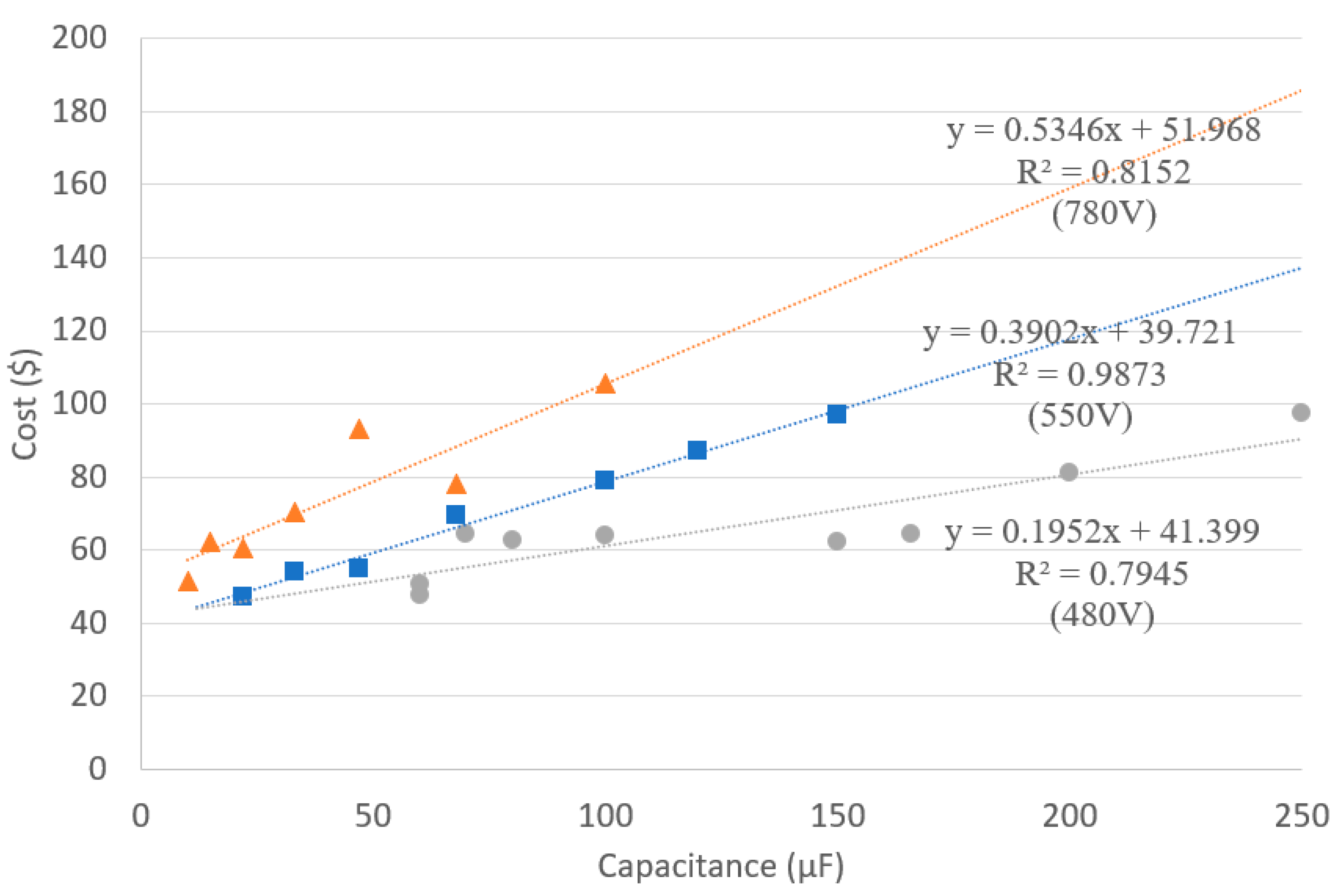
4.2. Cost Model of Capacitor

4.2.1. Cost Model of DC-Link Capacitor

The 3-leg inverter and 4-leg inverter have one electrolytic capacitor as a DC-link capacitor. Both inverters should analyze a product family of 600 V or higher, taking into account the voltage applied to the DC-link capacitor. However, due to the lack of samples of commercial products for high voltage electrolytic capacitors, prices are compared using TDK Electronics’ 300 V, 400 V and 500 V product lines. A serial combination of capacitors can satisfy the working voltage and a parallel combination of capacitors can satisfy the required capacitance.
Figure 18 shows the cost model of an electrolytic capacitor. As the capacitance increases, the cost of the electrolytic capacitor increases linearly, as expressed in (10)–(12).
σ C _ d c l i n k 300 V = 9.956 x + 15.023
σ C _ d c l i n k 400 V = 12.153 x + 19.921
σ C _ d c l i n k 500 V = 21.109 x + 22.168
where x is the capacitance (mF) of the DC-link capacitor.

4.2.2. Cost Model of Filter Capacitor

The filter capacitor is analyzed based on the film capacitor. The rated voltage applied to the filter capacitor for both inverters is 380 V. Therefore, a cost model is generated by using the product line of 480 V, 550 V, and 780 V of KEMET considering voltage margin. As shown in Figure 19, the cost of increasing the capacitance of the film capacitor is linear, as expressed in (13)–(15).
σ C _ f i l m 480 V = 0.1952 x + 41.399
σ C _ f i l m 455 V = 0.3902 x + 39.721
σ C _ f i l m 780 V = 0.5346 x + 51.968
where x is the capacitance (μF) of the film capacitor.

4.3. Cost Model of Filter Inductor

The 3-leg inverter has three filter detectors, and the 4-leg inverter has three filter inductors and one neutral inductor. Unlike other parts, inductors do not have an appropriate distribution of products on the market. Therefore, we estimate the cost model from the sum of the price of core and wire. The core size and AWG of the wire required the design of the filter inductor with reference to [33] and the core cost model is shown in (16).
Figure 20a shows the core price per available magnetizing area (Ae) of TDK Electronics’ toroidal core. As the Ae of the core increases, the price increases as an exponential function and is expressed in (16).
σ L _ c o r e Ae = 5.6424 e 0.007 x
where x means the Ae value of the core suitable for the filter inductor. Next, the AWG of the wire used in the filter inductor and the number of turns according to AL-value are considered [33]. When the number of turns of the inductor is determined, the wire diameter is calculated from (17). Here ρc is the electrical resistance of the copper wire, lT is the mean-length per turn (MLT) of the windings, and Pcu is the amount of heat or energy wasted when the current flows.
d 2 π I S ρ c l T N P c u w h e r e , N = L A L v a l u e
To reduce skin effect and proximity effect losses in conductors, a copper-braid form, which is many thin wire strands individually insulated and twisted or woven together such as Litz wire, can be applied. However, since the wire price is calculated as part of the inductor price, we consider the AWG of a single wire for convenience.
Figure 20b shows the price per meter per AWG of copper wire. As the wire thickens, the price per meter of the wire increases as an exponential function. The price per meter per AWG is given as (18).
σ L _ w i r e = 2.0277 e 0.23 x

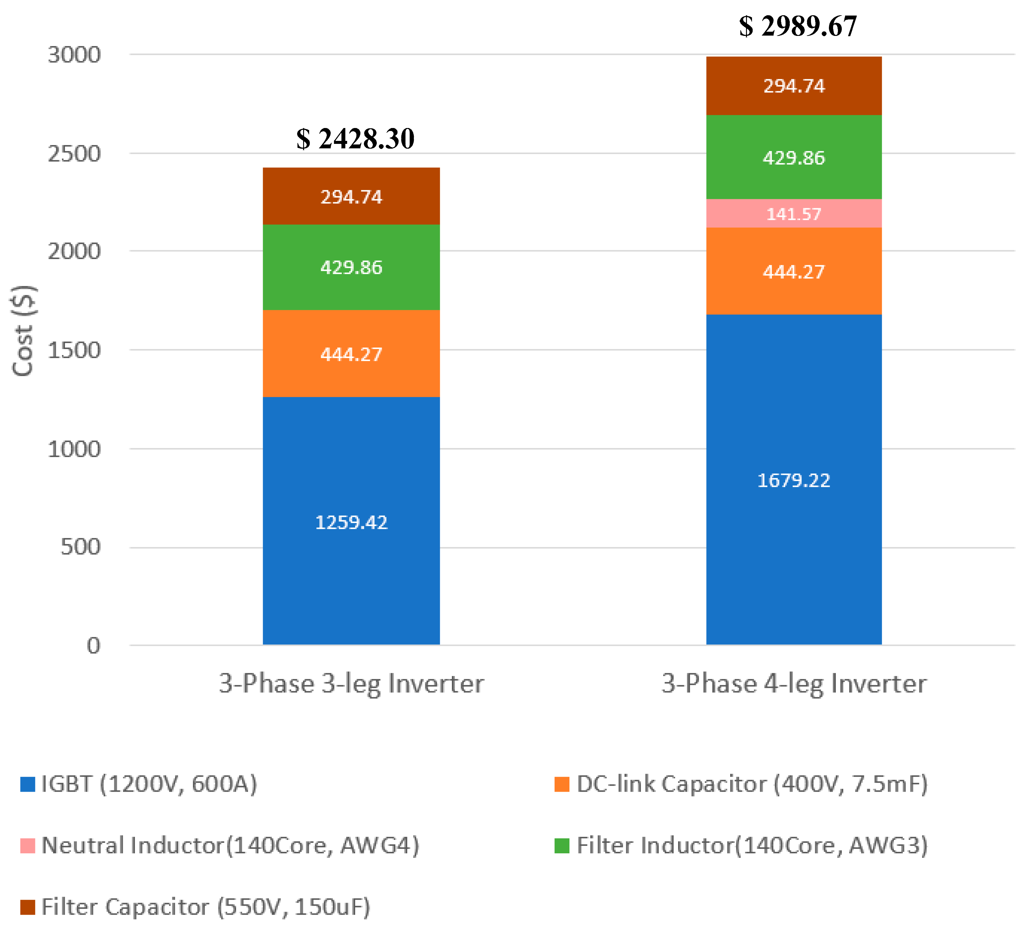
4.4. Cost Comparison of the Inverter Using the Part Cost Model

In this section, the price of a 3-leg inverter and a 4-leg inverter are compared using the part cost model. The 3-leg requires six IGBTs and the 4-leg inverter needs eight IGBTs. An IGBT has 1200 V and 600 A ratings. The voltage applied to the DC-link capacitor of the two inverters is 600 V. To meet the working voltage, connect four 7.5 mF capacitors with a working voltage of 400 V in series parallel. Thus, the working voltage of the DC-link capacitor is 800 V and the capacitance is 15 mF. The applied voltage of the filter inductor is 380 V. It uses film capacitors with a voltage rating of 550 V and capacitance of 150 μF with a voltage margin of about 1.5 times higher. In the case of inductors, the voltage applied to the filter and the neutral inductor is the same, but the required inductance is different. Since the minimum size of the filter inductor core meeting the output power capacity is 131 mm, the design uses a T140 × 103 × 25 core of AL-value 1100 nH. We calculate the number of turns required for a filter inductor and a neutral inductor, derive the AWG and calculate the price of the wire by multiplying the price per meter of the wire with the turns and MLT (mean-length per turn).
The comparison of the 3-leg inverter and 4-leg inverter using the part cost model is shown in Figure 21. Comparing the price of two inverters with the design conditions of Table 1 results in a price difference of about USD 561. This is the result of the difference in the number of neutral inductors and the number of IGBTs. The price comparison in Figure 21 does not take into account all the parts, design and manufacturing costs of the inverter. A more accurate price comparison will be possible, considering that 4-leg inverters can increase program coding costs and increase additional design costs for controllers compared to 3-leg inverters.

5. Conclusions

For 3-leg inverters and 4-leg inverters to which SVPWM control is applied, this paper analyzes the failure rate and MTBF based on a fault-tree and compares the price of the inverters. Because PCA is a reliability assessment that only takes into account the type, number and connection status of parts, the failure rate usually increases as the number of parts increases. However, the FTA results show a high failure rate in the order of split DC-link capacitor 3-leg inverter > 3-leg inverter > 4-leg inverter. In general, the 4-leg inverter with the largest number of parts should have the highest failure rate, but the redundancy effect significantly reduced the failure rate. For more accurate failure rate prediction, the failure rate and MTBF of the 4-leg inverter according to the lifecycle of the controller were analyzed. The MTBF of the controller shall be guaranteed for at least 10 years in order for the 4-leg inverter to secure MTBF of approximately eight years in the 25 °C operating conditions.
In conclusion, the 4-leg inverter has a price increase of USD 561 at the same power capacity compared to the 3-leg inverter, but reliability is greatly improved by enabling the operation of redundancy compensation while also enabling the adjustment of the energy flow or output voltage in unbalanced load conditions.

Author Contributions

Conceptualization, S.-G.S. and F.-s.K.; Data curation, Y.-g.K. and F.-s.K.; Formal analysis, Y.-g.K., D.-h.H. and F.-s.K.; Investigation, Y.-g.K., D.-h.H., S.-P.K., S.-J.P. and F.-s.K.; Methodology, S.-G.S. and F.-s.K.; Project administration, F.-s.K.; Resources, S.-J.P.; Software, F.-s.K.; Supervision, F.-s.K.; Validation, S.-P.K. and F.-s.K.; Visualization, F.-s.K.; Writing—original draft, F.-s.K.; Writing—review & editing, S.-G.S., S.-J.P. and F.-s.K. All authors have read and agreed to the published version of the manuscript.

Funding

This work was supported by the Korea Institute of Energy Technology Evaluation and Planning (KETEP) grant funded by the Korea government (MOTIE) (20194310100030, Development of Demonstration Zone for New Electricity Service Model).

Institutional Review Board Statement

Not applicable.

Informed Consent Statement

Not applicable.

Data Availability Statement

Data is contained within the article.

Conflicts of Interest

The authors declare no conflict of interest.

References

  1. Douglass, P.J.; Trintis, I.; Munk-Nielsen, S. Voltage unbalance compensation with smart three-phase loads. In Proceedings of the Power Systems Computation Conference, PSCC 2016, Genoa, Italy, 20–24 June 2016; pp. 1–7. [Google Scholar]
  2. Hu, J.; Fu, X.; Liao, T.; Chen, X.; Ji, K.; Sheng, H.; Zhao, W. Low Voltage Distribution Network Line Loss Calculation Based on The Theory of Three-phase Unbalanced Load. In Proceedings of the 3rd International Conference on Intelligent Energy and Power Systems, IEPS 2017, Hangzhou, China, 10 October 2017; pp. 65–71. [Google Scholar]
  3. Lin, F.; Tan, K.; Lai, Y.; Luo, W. Intelligent PV Power System with Unbalanced Current Compensation Using CFNN-AMF. IEEE Trans. Power Electron. 2019, 34, 8588–8598. [Google Scholar] [CrossRef]
  4. Han, J.; Oh, Y.S.; Gwon, G.H.; Kim, D.U.; Noh, C.H.; Jung, T.H.; Lee, S.J.; Kim, C.H. Modeling and Analysis of a Low-Voltage DC Distribution System. Resources 2015, 4, 713–735. [Google Scholar] [CrossRef] [Green Version]
  5. Wang, J.; Konikkara, D.D.; Monti, A. A generalized approach for harmonics and unbalanced current compensation through inverter interfaced distributed generator. In Proceedings of the IEEE 5th International Symposium on Power Electronics for Distributed Generation Systems, PEDG 2014, Galway, Ireland, 24–27 June 2014; pp. 1–8. [Google Scholar]
  6. Bifaretti, S.; Lidozzi, A.; Solero, L.; Crescimbini, F. Comparison of modulation techniques for active split dc-bus three-phase four-leg inverters. In Proceedings of the IEEE Energy Conversion Congress and Exposition, ECCE 2014, Pittsburgh, PA, USA, 14–18 September 2014; pp. 14–18. [Google Scholar]
  7. Lin, Z.; Ruan, X.; Jia, L.; Zhao, W.; Liu, H.; Rao, P. Optimized Design of the Neutral Inductor and Filter Inductors in Three-Phase Four-Wire Inverter With Split DC-Link Capacitors. IEEE Trans. Power Electron. 2019, 34, 247–262. [Google Scholar] [CrossRef]
  8. Liu, Z.; Liu, J.; Li, J. Modeling, Analysis, and Mitigation of Load Neutral Point Voltage for Three-Phase Four-Leg Inverter. IEEE Trans. Ind. Electron. 2013, 60, 2010–2021. [Google Scholar] [CrossRef]
  9. Hadidian Moghaddam, M.J.; Kalam, A.; Miveh, M.R.; Naderipour, A.; Gandoman, F.H.; Ghadimi, A.A.; Abdul-Malek, Z. Improved Voltage Unbalance and Harmonics Compensation Control Strategy for an Isolated Microgrid. Energies 2018, 11, 2688–2714. [Google Scholar] [CrossRef] [Green Version]
  10. Chee, S.J.; Kim, H.S.; Sul, S.K.; Ko, S. Common-Mode Voltage Reduction of Three-Level Four-Leg PWM Converter. IEEE Trans. Ind. Appl. 2015, 51, 4006–4016. [Google Scholar] [CrossRef]
  11. Zhang, R.; Prasad, V.H.; Boroyevich, D.; Lee, F.C. Three-dimensional space vector modulation for four leg voltage source converters. IEEE Trans. Power Electron. 2002, 17, 314–326. [Google Scholar] [CrossRef]
  12. Aissani, M.; Aliouane, K. Three-dimensional space vector modulation for four-leg voltage-source converter used as an active compensator. In Proceedings of the International Symposium on Power Electronics, Electrical Drives, Automation and Motion, SPEEDAM 2010, Pisa, Italy, 14–16 June 2010; pp. 1416–1421. [Google Scholar]
  13. Golwala, H.; Chudamani, R. New Three-Dimensional Space Vector-Based Switching Signal Generation Technique without Null Vectors and With Reduced Switching Losses for a Grid-Connected Four-Leg Inverter. IEEE Trans. Power Electron. 2016, 31, 1026–1035. [Google Scholar] [CrossRef]
  14. Zhang, Q.; Zhang, P.; Zhao, S.; Gao, J.; Sun, X. Research on a discontinuous three-dimensional space vector modulation strategy for the three-phase four-leg inverter. In Proceedings of the IEEE 8th International Power Electronics and Motion Control Conference, IPEMC-ECCE Asia 2016, Hefei, China, 22–26 May 2016; pp. 575–580. [Google Scholar]
  15. Llonch-Masachs, M.; Heredero-Peris, D.; Montesinos-Miracle, D.; Rull-Duran, J. Understanding the three and four-leg inverter Space Vector. In Proceedings of the 18th European Conference on Power Electronics and Applications, EPE ECCE Europe 2016, Karlsruhe, Germany, 5–9 September 2016; pp. 1–10. [Google Scholar]
  16. Kim, J.H.; Sul, S.K. A carrier-based PWM method for three-phase four-leg voltage source converters. IEEE Trans. Power Electron. 2004, 19, 66–75. [Google Scholar] [CrossRef]
  17. Kim, J.H.; Sul, S.K.; Kim, H.; Ji, J.K. A PWM strategy for four-leg voltage source converters and applications to a novel line interactive UPS in a three phase four wire system. In Proceedings of the 39th IEEE Industry Applications Conference, IAS 2004, Seattle, WA, USA, 3–7 October 2004; pp. 2202–2209. [Google Scholar]
  18. Kim, S.Y.; Song, S.G.; Park, S.J. Minimum Loss Discontinuous Pulse-Width Modulation Per Phase Method for Three-Phase Four-Leg Inverter. IEEE Access 2020, 8, 122923–122935. [Google Scholar] [CrossRef]
  19. Gamini Jayasinghe, S.D.; Mahinda Vilathgamuwa, D.; Madawala, U.K. A Dual Inverter-Based Supercapacitor Direct Integration Scheme for Wind Energy Conversion Systems. IEEE Trans. Ind. Appl. 2013, 49, 1023–1030. [Google Scholar] [CrossRef]
  20. Reliability prediction of electric equipment. In Rep. MIL-HDBK-217F; Department of Defense, Washington DC, Tech.: Washington, DC, USA, 1991; Available online: http://everyspec.com/MIL-HDBK/MIL-HDBK-0200-0299/MIL-HDBK-217F_14591 (accessed on 3 January 2021).
  21. Choudhary, K.; Sidharthan, P. Reliability Prediction of Electronic Power Conditioner (EPC) using MIL-HDBK-217 based Parts Count Method. In Proceedings of the International Conference on Computer, Communication and Control, IC4 2015, Indore, India, 10–12 September 2015. [Google Scholar]
  22. Mou, H.; Hu, W.; Sun, Y.; Zhao, G. A Comparison and Case Studies of Electronic Product Reliability Prediction Methods Based on Handbooks. In Proceedings of the International Conference on Quality, Reliability, Risk, Maintenance, and Safety Engineering, QR2MSE 2013, Chengdu, China, 15–18 July 2013; pp. 112–115. [Google Scholar]
  23. Jones, J.; Hayes, J. A comparison of electronic-reliability prediction models. IEEE Trans. Reliab. 1999, 48, 127–134. [Google Scholar] [CrossRef]
  24. Yeo, S.C.; Kang, F.S. Fault-Tree Based Failure-Rate Analysis for Boost Converter and Interleaved Boost Converter. J. Electr. Eng. Technol. 2019, 14, 2375–2387. [Google Scholar] [CrossRef]
  25. Kang, F.S.; Song, S.G. Fault-Tree Based Failure-Rate Analysis for Clamped-double Submodule employing dc-short current protecting function. J. Electr. Eng. Technol. 2020, in press. [Google Scholar] [CrossRef]
  26. Khalil, M.; Soulatiantork, P. Reliability assessment of PV inverters. In Proceedings of the 14th IMEKO TC10 Workshop Technical Diagnostics, New Perspectives in Measurements, Tools and Techniques for System’s Reliability, Maintainability and Safety 2016, Milan, Italy, 27–28 June 2016; pp. 389–393. [Google Scholar]
  27. Shoults, L.W. Implementation of Design Failure Modes and Effects Analysis for Hybrid Vehicle Systems. Master’s Thesis, Virginia Polytechnic Institute and State University, Blacksburg, VA, USA, May 2016. [Google Scholar]
  28. Basu, J.B. Failure Modes and Effects Analysis (FMEA) of a Rooftop PV System. Int. J. Sci. Eng. Res. 2015, 3, 51–55. [Google Scholar]
  29. MIL-STD-1629A, Procedures for Performing a Failure Mode, Effects and Criticality Analysis, November 1980. Available online: https://www.fmea-fmeca.com/milstd1629.pdf (accessed on 3 January 2021).
  30. IEC-60182, Analysis Techniques for System Reliability-Procedure for Failure Mode and Effects Analysis (FMEA). 2006. Available online: https://webstore.iec.ch/preview/info_iec60812%7Bed2.0%7Den_d.pdf (accessed on 3 January 2021).
  31. Burkart, R.; Kolar, J.W. Component cost models for multi-objective optimizations of switched-mode power converters. In Proceedings of the IEEE Energy Conversion Congress and Exposition ECCE 2013, Denver, CO, USA, 15–19 September 2013; pp. 2139–2146. [Google Scholar]
  32. Domingues-Olavarría, G.; Fyhr, P.; Reinap, A.; Andersson, M.; Alaküla, M. From Chip to Converter: A Complete Cost Model for Power Electronics Converters. IEEE Trans. Power Electron. 2017, 32, 8681–8692. [Google Scholar] [CrossRef]
  33. Valchev, V.C.; Bossche, A.V. Inductors and Transformers for Power Electronics, 1st ed.; CRC Press: Boca Raton, FL, USA, 2005; pp. 33–42. [Google Scholar]
Figure 1. Circuit configuration of three-phase 3-leg inverter.
Electronics 10 00087 g001
Figure 2. Circuit configuration of three-phase 3-leg inverter employing split DC-link capacitors.
Electronics 10 00087 g002
Figure 3. Circuit configuration of three-phase 4-leg inverter.
Electronics 10 00087 g003
Figure 4. Photograph of three-phase 4-leg inverter: (a) Power stage; (b) controller.
Electronics 10 00087 g004
Figure 5. Failure dependency of three-phase 3-leg inverter.
Electronics 10 00087 g005
Figure 6. Failure dependency of three-phase 3-leg inverter with split DC-link capacitors.
Electronics 10 00087 g006
Figure 7. Failure dependency of 4-leg inverter.
Electronics 10 00087 g007
Figure 8. Comparison of failure rate and mean time between failures (MTBF) by part count failure analysis (PCA): (a) Failure rate; (b) mean time between failures.
Electronics 10 00087 g008
Figure 9. Fault-tree of three-phase 3-leg inverter.
Electronics 10 00087 g009
Figure 10. Fault-tree of three-phase 3-leg inverter with split DC-link capacitors.
Electronics 10 00087 g010
Figure 11. Fault-tree of three-phase 4-leg inverter.
Electronics 10 00087 g011
Figure 12. Phase current (ia, ib, ic) and neutral current (in) of three-phase 4-leg inverter: (a) With three-phase balanced load condition; (b) when the load of phase A is half of the phase B and C loads by load imbalance; (c) when the load of phase C doubles phases A and B due to load imbalance; (d) alternate operation of the additional switch arm due to failure of phase C.
Electronics 10 00087 g012
Figure 13. Comparison of failure rate and MTBF by fault-tree analysis (FTA): (a) Failure rate; (b) mean time between failures, year.
Electronics 10 00087 g013
Figure 14. Failure rate and MTBF of 3-leg inverter according to the controller lifecycle: (a) Failure rate; (b) mean time between failures, year.
Electronics 10 00087 g014
Figure 15. Failure rate and MTBF of split-DC-link capacitor 3-leg inverter according to the controller lifecycle: (a) Failure rate; (b) mean time between failures, year.
Electronics 10 00087 g015
Figure 16. Failure rate and MTBF 4-leg inverter according to the controller lifecycle: (a) Failure rate; (b) mean time between failures, year.
Electronics 10 00087 g016
Figure 17. Cost model of IGBT.
Electronics 10 00087 g017
Figure 18. Cost model of electrolytic capacitor.
Electronics 10 00087 g018
Figure 19. Cost model of film capacitor.
Electronics 10 00087 g019
Figure 20. Cost model of inductor: (a) Core price per available magnetizing area, Ae; (b) wire price according to AWG.
Electronics 10 00087 g020
Figure 21. Cost comparison of 3-leg and 4-leg inverters using the cost model of the part.
Electronics 10 00087 g021
Table 1. Specifications of three-phase 4-leg inverter.
ItemValues
Output power100 kW
Output voltage (line-to-neutral)380 V, 60 Hz
DC-link voltage600 V
DC-link capacitance15.5 mF
Switching deviceIGBT CM600HA-24H
ac filter for A, B, C phase legs660 μH
ac filter inductor for neutral leg330 μH
ac filter capacitor for each phase150 μH
Table 2. Failure rate of [Switching signal generation function failure] corresponding to MTBF.
MTBF (Year)MTBF (Day)MTBF (h)Failure Rate (Failures/104h)
3109526,2800.380517504
5182543,8000.228310502
10365087,6000.114155251
155475131,4000.076103501
207300175,2000.057077626
Publisher’s Note: MDPI stays neutral with regard to jurisdictional claims in published maps and institutional affiliations.

