Abstract
This paper presents new architectures and implementations of original open-loop Class-BD audio amplifiers with balanced Common-Mode output. The output stage of each proposed amplifier includes the typical H-bridge with four MOSFETs and four additional MOSFET switches that balance and keep the Common-Mode output constant. The presented amplifiers employ the extended NBDD PWM or PSC PWM modulation scheme. When the output stage is built only on NMOSFET transistors, gate drivers require a floating power supply, using a self-boost charge pump with capacitive isolation of the control signal. The use of complementary MOSFETs in the output stage greatly simplifies gate control systems. The proposed amplifiers were compared to the typical Class-BD configuration, using the optimal NBDD modulation with respect to audio performance of the Differential-Mode (DM) and Common-Mode (CM) outputs. Basic SPICE simulations and experimental studies have shown that the proposed Class-BD amplifiers have similar audio performance to the prototype with the optimal NBDD modulation scheme, while at the same time having a balanced constant voltage CM output, thus eliminating the main contributor to radiation emission. As a result, the filtering of the DM output signals can be greatly simplified, while the filtering of the CM output signals can be theoretically eliminated. Practically, due to the timing errors added by the gate drivers, spikes are generated at the CM output, which are very easy to filter out by the reduced LC output filter, even at very low L.
1. Introduction
Many works have been dedicated to different kinds of improved PWM methods and Class D power amplifier topologies in order to achieve two of the most important features: high fidelity and high efficiency.
Class-D amplifier architectures can generally be divided into two categories: open-loop Class-D amplifiers with natural pulse width modulation (NPWM), or its discrete-time version known as uniform PWM (UPWM); and closed-loop ones with Sigma–Delta modulation (SDM) and bang–bang control modulation.
Depending on the sampling method, PWM schemes are generally categorized in three of the most important classes: natural NPWM, uniform UPWM and linearized PWM (LPWM) [1,2].
In addition, each PWM sampling method also distinguishes one-edge or two-edge PWM, as well as two-level (Class-AD) or three-level (Class-BD) switching. Among four fundamental NPWM schemes, NBDD (Natural sampling Class-BD Double sided) modulation, which is equivalent to the level-three version of Phase Shifted Carrier Pulse Width Modulation (PSC PWM) [1,2], is the best in terms of the DM output and has by far the most attractive spectral characteristic, which contains much less unwanted spectral components than all other PWM methods.
The H-bridge output stage of the Class-BD amplifier with the appropriate NBDD modulator and time domain waveforms of the control signals and output voltages are shown in Figure 1.
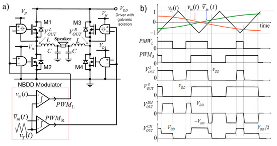
Figure 1.
Class-BD amplifier, using NBDD PWM modulator: (a) Block diagram; (b) time domain waveforms of: NBDD output signals and voltages at DM and CM outputs.
The control signals contain dead time between the switch states where all switches are off to achieve zero voltage switching (ZVS) and to prevent shoot-through currents.
The DM and CM outputs of the NBDD modulation can be expressed after some conversion by the following Double Fourier Series (DFS) expressions [1,2,3]:
where —switching angle frequency, —audio angle frequency, M—modulation index, , —Bessel function of n-th order.
Equation (1) shows that effective sampling frequency of the DM output signal is doubled without increasing the transition frequency on the output, and all harmonics around odd multiples of the switching frequency are eliminated. However, the CM output (Equation (2)) reveals some drawback, as the frequency spectrum of the NBDD output contains the odd harmonics of the switching frequency and their even intermodulation (IM) components. The CM output components are present at full scale, even at a very low level of the modulating signal.
Fast switching of the output transistors, nearly rail-to-rail high swings, and wide frequency spectrum of PWM signals can lead to high-frequency RF emissions and interference from the output stage, printed circuit board traces, filter and speaker cables, which become inadvertent antennas [4,5,6,7].
A properly designed external LC filter, placed as close as possible to the switching output stage, suppresses the unwanted RF effects, limits the amount of the output ripple current, protects the speaker by attenuating the switching frequency, and also reduces EMI [8,9,10]. The LC filter for the Class-BD amplifier with NBDD modulation must be designed separately for DM and CM components. Filtration of unwanted components of the spectrum at the DM output is very easy because the NBDD frequency spectrum has no harmonics of the switching frequency, and no IM components around odd multiples of the switching frequency. In terms of DM output, NBDD is the best and has, by far, the most attractive spectral characteristics for all the other NPWM methods.
However, the frequency spectrum of the NBDD CM output contains the odd harmonics of the switching frequency, and their even IM components (2). The CM output components are present at full scale, even at a very low level of the modulating signal. The IM components around the first harmonic of the switching frequency are the most undesirable because they put strong demands on the CM output signals filtering. The output filter of the Cass-BD amplifier uses, most often, a common mode choke coil instead of two normal inductors, which results in more effective CM output signal suppression because the CM choke coil exhibits much larger impedance for the CM output current than for the DM one [9,10].
In the last decade, filterless Class-D amplifiers have become very popular [10,11,12]. The output of the filterless Class-D amplifier is directly connected to a load (speaker), and the load itself provides filtering.
In many recent studies, the theory behind PWM and different modulation schemes, as well as new linearization methods, have been discussed; thus, high-fidelity improvements and EMI reduction of the filterless Class-D amplifiers have been proposed [6,7,12,13,14,15,16].
An original, Common-Mode Free BD (CMFBD) modulation that keeps the CM output constant is presented in [7]. The DM output of this amplifier has the same performance as that using the optimal NBDD modulation; however, the switching frequency of the power MOSFETs creating the new H-bridge output stage is doubled. A detailed analysis of the presented CMFBD modulation shows that it is equivalent to the Phase Shifted Carrier Pulse Width Modulation (PSC PWM) that is considered as a multi-level PWM method for Class-BD amplifiers [1,2].
Figure 2 shows the circuit diagram of the Class-BD output stage, using the PSCPMW modulation scheme and the block diagram of the PSC PWM modulator that generates all control S1–S3 signals [2,7]. The H-bridge contains two additional series switches, M5 and M6, connected parallel with the load, which are used to shunt the bi-directional inductive load current when M1–M4 are off and to set both outputs at with the help of shunt resistor Rb connected parallel with M1–M4 transistors. The DM and CM outputs of the PSC PWM modulation can be expressed after some conversion by the following DFS expressions [2,3]:
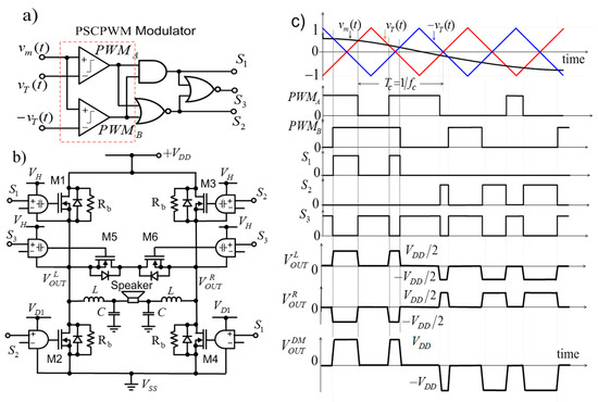
Figure 2.
Class-BD amplifier based on PSC PWM modulation scheme: (a) Block diagram of PSC PWM modulator; (b) the output stage; (c) time domain waveforms at the outputs of the modulator and amplifier.
Comparing Equations (1) and (2) with the corresponding Equations (3) and (4), as well as Figure 1b with Figure 2c, we can see that the DM output of the Class-BD amplifier with the PSC PWM modulation is identical to that one for the optimal NBDD PWM; however, PSC PWM keeps the CM output constant.
The disadvantage of PSC PWM modulation is the need to use two additional series switches, M5 and M6, as well as switching power transistors with twice the frequency of NBDD modulation, which results in higher switching power losses. In addition, power losses occur in shunt resistors Rb connected in parallel with the M1–M4 to set both outputs at , which also increase the rise and fall times of the PWM output pulses, contributing to a further increase in switching power losses.
The organization of this paper is as follows. Section 2 presents original architectures and implementations of Class-BD audio amplifiers with the balanced CM output. The output stage of each proposed amplifier includes the typical H-bridge with four MOSFETs and four additional MOSFET switches that balance and keep the Common-Mode output constant. The presented amplifiers employ the extended NBDD PWM or PSC PWM modulation schemes. Section 3 presents basic SPICE simulations and experimental studies of the proposed Class-BD amplifiers implemented on the complementary MOSFET pairs. Conclusions are given in Section 4.
2. Class-BD Amplifiers with Balanced CM Output Employing the Extended NBDD PWM or PSC PWM Modulation Scheme
Figure 3a shows a slightly improved version of the Class-BD audio amplifier with a balanced CM output [3], using the extended NBDD PWM modulator (Figure 3c).
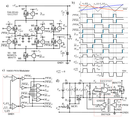
Figure 3.
Class-BD audio amplifier with balanced CM output, using the extended NBDD PWM modulator: (a) Topology of the output stage, (b) time domain waveforms at the outputs of the modulator and amplifier. (c) Block diagram of the extended NBDD PWM modulator. (d) Floating gate driver with galvanic isolation of the control signal.
This amplifier consists of a typical H-bridge output stage with four MOSFETs, and four additional MOSFET switches (M5, M6 and M7, M8), separating the H-bridge from the power supply, and switching the bridge’s power rails to the half-voltage VDD/2, at the time intervals in which the MOSFETs of the high-side or the low-side of the H-bridge are closed simultaneously. At these states, when M1, M3 transistors of the high-side are on, M7 is off and M8 is on, whereas when M2, M4 transistors of the low-side are on, M5 is off and M6 is on. The switching frequency of all MOSFETs is the same as for NBDD modulation, i.e., twice as low as that for PSC PWM modulation as shown in Figure 2b.
When all gate drivers UCC27537 have the same turn-on and turn-off propagation delays (according to the datasheet, it is 17 ns), the modulated PWM waveform at the H-bridge output is undistorted and is only delayed in relation to the control signals. These delays do not have to be the same, as it is necessary to introduce an appropriate delay time on the rising edges of all control signals turning on the MOSFETs, with respect to the falling edges of all control signals turning off the MOSFETs. This allows a zero-switching voltage to be achieved to prevent shoot-through currents during switching processes; however, dead time in particular has the most significant contribution of nonlinearity in the H-bridge output. The optimal turn-on delay time for MOSFETs is a compromise between low shoot-through currents and low switching power losses, and an acceptable THD level at the output of the class D amplifier.
To implement this delay, an input AND gate with two Schmitt Trigger inputs of the UCC27537 were used (Figure 3c). Time constant Rd Cd of the circuit connected to one of the inputs of this gate determines the appropriate delay time on the rising edges of control signal turning on the MOSFET. The gate driver output is connected to the gate of the transistor via a resistor RG and an anti-parallel Schottky diode, providing turn-off speed enhancement. The ground GND1 of the PWM controller is isolated from the floating ground GND of the driver, using the digital isolator ISO7420 with an insulating barrier made of silicon dioxide (SiO2).
Figure 3c also shows a self-boost charge pump circuit [16], generating the floating power supply for the gate driver of the M2 transistor; the same solution applies to all other MOSFETs. Continuous switching of MCP1 ensures that the isolated and floating charge pump bias supply is available at all times to the corresponding driver, regardless of the modulation index M and without any interference with the desired phase-leg switching sequence.
Much simpler solutions for gate control systems can be used when the output stage of the amplifier is implemented on complementary MOSFET pairs.
As shown in Figure 4, the gate drivers of all MOSFETs share a common ground GND1 and are directly driven from the NBDD modulator outputs. The block diagram of the NBDD PWM modulator is also simpler (Figure 4d) because the output stage implemented on complementary MOSFET pairs does not need pairs of complementary control signals.
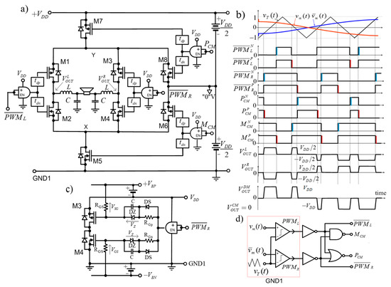
Figure 4.
Class-BD audio amplifier with balanced CM output, using the extended NBDD PWM modulator and implemented on complementary MOSFET pairs: (a) Topology of the output stage. (b) Time domain waveforms at the amplifier outputs, and PWM control signals with delayed turn-on times for the NMOS and PMOS transistors. (c) Implementation of the turn-on delay times of the NMOS and PMOS. (d) Block diagram of the extended NBDD PWM modulator.
Taking into account that M6 and M8 transistors are supplied with a half voltage , the supply voltage of this system should be within a limited range, described by the following inequalities:
At the higher gate voltage , the drain to source resistance in the on state is less than a certain value at which the conduction power losses are still acceptable. and are the maximum values for complementary MOSFETs, the most common , which result in the following condition: . Therefore, it is not possible to use the supply voltage higher than : .
Figure 4c shows a gate drive circuit with a shifted reference voltage level for the control signals that is suitable for the applications with complementary power MOSFETs with the following supply voltage:
Shown in Figure 4c, the gate driver has the ability to control turn-on and turn-off speeds independently for NMOSFET and PMOSFET. The RG resistor allows adjustment of the MOSFET turn-on speed (RGn allows to adjust the delay time of the rising edges of the PWM signal, while RGp allows to adjust the delay time of the falling edges) independently. During turn-off, the antiparallel Schottky diode shunts out serial resistor RG; in addition, the gate charge is taken from the parallel CB capacitor charged to the Zener voltage VZ, providing turn-off speed enhancement. During the on-time of the switch, a small DC current flows in the level shifter, keeping the driver biased in the right state.
An original Class-BD audio amplifier with a balanced CM output, implemented on complementary MOSFET pairs and employing an extended PSC PWM modulation scheme, is shown in Figure 5a.
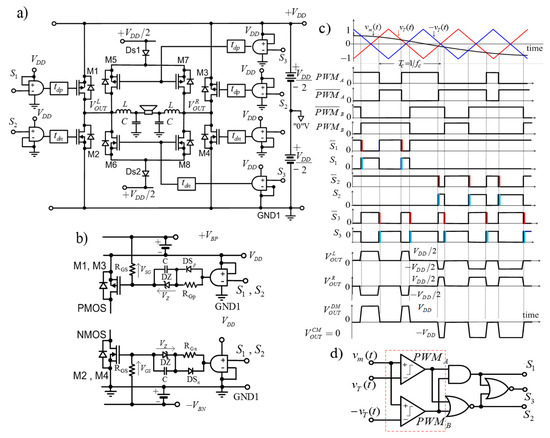
Figure 5.
Class-BD audio amplifier with balanced CM output, using PSC PWM modulation scheme. (a) A new topology of the output stage. (b) Implementation of the turn-on delay times of the NMOS and PMOS. (c) Time domain waveforms at the amplifier outputs and PWM control signals with delayed NMOS and PMOS turn-on times (directly at the gates of these transistors). (d) Block diagram of the extended PSC PWM modulator.
Figure 5b shows the voltage waveforms at the DM and CM outputs of the amplifier, as well as logical combinations of the control signals with delayed turn-on times for the NMOS and PMOS transistors. Additionally, in this case, the use of complementary transistors in the power stage significantly simplify their control because the gate drivers of all MOSFETs share a common ground GND1 and are directly driven from the extended PSC PWM modulator outputs.
Instead of shunting resistors Rb to set both outputs at (as in Figure 2b), an additional H-bridge was created by M5, M7 and M6, M8 transistors; however, the lower and upper sides of the new H-bridge are connected to the same power supply via oppositely polarized Schottky diodes. Two parallel branches of the serial-connected two NMOSFETs (M6, M8) or PMOSFETs (M5, M7) are connected parallel with the load, and are used to shunt the bi-directional inductive load current when M1–M4 are off and to set both outputs at . The same implementation of the turn-on delay times of the NMOS and PMOS transistors, as shown in Figure 4c, allows to adjust the delay time of the rising and falling edges of the PWM signal independently. The architecture presented in Figure 5a can be implemented using only NMOSFETs, but galvanic isolation in the transmission path of the control signals as well an isolated and floating bias power supply for gate drivers must be provided.
3. Simulation and Measurement Results
SPICE simulations and experimental studies were used to compare the parameters of the proposed class BD amplifiers with a balanced CM output with a prototype, using an optimal NBDD modulation scheme. All Class-BD amplifiers were tested for two different switching frequencies: or , using with each switching frequency two different sets of load resistance as well as the parameter values of the LC output filter: (1) RL = 4 Ω, L = 15 µH, C = 1.8 µF; (2) RL = 8 Ω, L = 30 µH, C = 1 µF [8].
Since the proposed amplifiers in Figure 4 and Figure 5 are built on complementary MOSFETs, and the applied supply voltage VDD = 24 V exceeds the VGSmax voltage (inequality 6), it was necessary to use a voltage level shifting circuit with a Zener diode (VZ = 6.2 V) to lower the control voltage from the gate driver output (with the exception of MOSFETs, whose sources are connected to the half voltage VDD/2—i.e., Virtual GND “0” V).
Figure 6a,b show the time waveforms of the PWM control signals generated in one selected period Tc, as well as the drain currents I(M1:D)–I(M4:D) and I(M5:D)–I(M8:D) of the power MOSFETs in Figure 4 and Figure 5, respectively. Optimal turn-on delay times of the transistors were adjusted by selecting the resistance values RGn and RGp (Figure 4c and Figure 5b). In our design, for RGp = 68 Ω and RGn = 150 Ω, we obtain the optimal turn-on delay times of the transistors and significant limitation of the shoot-through currents.
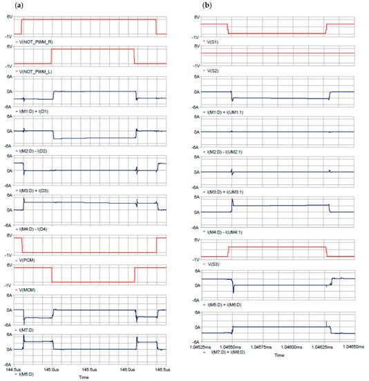
Figure 7a–c shows the efficiency and the output power versus modulation index M as well as THD as a function of the signal frequency for three Class-BD amplifiers: Figure 7a, shown in Figure 1 with the conventional NBDD modulator; Figure 7b, shown in Figure 4 with the extended NBDD PWM modulator; and Figure 7c, shown in Figure 5 with the extended PSC PWM modulator. These characteristics were determined for two different switching frequencies, with two sets of load resistance value as well as LC output filter parameter values, for each frequency. As we can see, the output power characteristics of all three amplifiers are almost identical, while the efficiencies of the two proposed amplifiers, containing four additional transistor switches to balance the CM outputs, are slightly lower to the efficiency of the prototype NBDD modulator amplifier, due to the additional power losses in the conduction states and in the switching processes of these additional transistor switches.
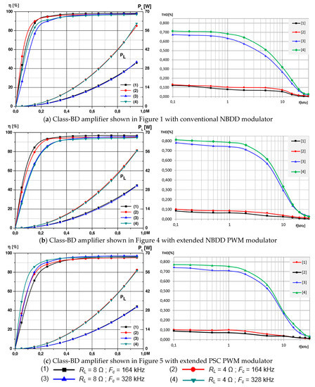
As we can see in Figure 7, all tested amplifiers show, however, slight distortions at the DM outputs, caused by distorted switching sequences generated by the output stages of these amplifiers. Switching timing error in a gate signal, due to turn-on delay times of the transistors, in particular, has the most significant contribution of nonlinearity in DM output stages. Based on Figure 7a–c, we can observe the following interesting properties. The proposed Class-BD amplifiers have a slightly higher THD than the prototype amplifier in Figure 1 with the conventional NBDD modulation. This is because the proposed amplifiers are controlled by modulators generating control signals with extended timing, giving more timing errors added in each switching period Tc by the gate drivers, such as dead time, and . THD of all tested amplifiers is higher for the higher switching frequency than for because relative timing errors are greater for shorter switching period Tc.
For example, Figure 8a–c shows the simulated THD + N frequency responses in the band up to 30 kHz for the three tested amplifiers at two switching frequencies and , modulating frequency , modulation index M = 0.95, load resistance RL = 8 Ω, and filter parameters L = 30 µH and C = 1 µF.
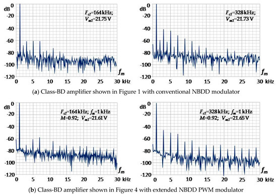
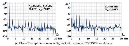
Figure 8.
Simulated THD + N frequency responses of three tested amplifiers in the band up to 30 kHz.
Figure 9 shows the voltage oscillograms measured at the following outputs of the proposed Class-BD amplifier with the PSC PWM modulator in Figure 5: right half bridge, left half bridge, DM output, and CM output before and after filtration. We obtain quite similar oscillograms for the Class BD-amplifier with the NBDD modulator in Figure 4. A comparison of the output voltages on the right half bridge, left half bridge and CM output, presented in Figure 5 and Figure 9, shows that the real-time waveforms are distorted by overlapping spikes on the rising and falling edges of the PWM pulse in each switching period. The main source of these spikes are timing errors added in each switching period Tc by the gate drivers, such as dead time. The inevitability of timing errors is due to the fact that the turn-on delay times of the NMOS and PMOS transistors have to be implemented by independently adjusting the delay times of the rising and falling edges of the PWM driving signals. Even with equal turn-on delay times of the NMOS and PMOS, during the dead time, the inductor current in the output LPF turns on the body diode. During the next phase when the other side of the MOSFET starts to turn on at the end of the dead time, the body diode stays in a conducting state unless the stored minority carrier is fully discharged. This reverse recovery current tends to have a sharp, spiky shape and leads to unwanted distortion by overlapping spikes on the rising and falling edges of the PWM pulse in each switching period. However, the filtration of the appearing spikes at the CM output is very easy, even when the filter inductance L is very small, as is shown in the oscillogram in Figure 9.
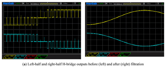
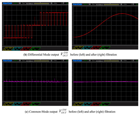
Figure 9.
Ocillograms measured at the following outputs of the Class-BD amplifier in Figure 5: (a) Left-half and right-half H-bridge outputs, (b) DM output, (c) CM output (in the left column before, in the right column after filtration); , ; vertically: 1 div/5 V; horizontally: 1 div/5 µs; .
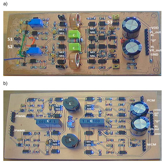
Figure 10 shows the PCBs of the tested Class-BD audio amplifiers with balanced CM output, implemented on complementary pairs HEXFET® Power MOSFET IRF9389PbF: (a) shown in Figure 4, using the extended NBDD PWM modulator; and (b) shown in Figure 5, using the extended PSC PWM modulator. To test a typical Class-BD amplifier in a H-bridge configuration with a classic NBDD PWM modulator (as shown in Figure 1 but with complementary MOSFETs), the main H-bridge of the amplifier in Figure 10a was used. To implement such a configuration, pins: drain-source of M5, M7 transistors should be galvanically connected, while M6 and M8 should be permanently open. Electronic components on PCBs have the same symbols as in Figure 4 and Figure 5. Load resistances of 4 Ω, 65 W or 8 Ω, 35 W are attached to PCBs with short cables from the outside.
The following set of equipment was used to test the amplifiers:
- −
- Rigol DG1032Z function generator;
- −
- Rigol DSA832E spectrum analyzer, 9 kHz ~ 3.2 GHz;
- −
- Hp 8593 agilent spectrum analyzer, 1 kHz ~ 2.9 GHz;
- −
- DSO4254B advanced digital oscilloscope 4 × 250 MHz.
4. Final Conclusions
Two original open-loop Class-BD audio amplifiers with balanced Common-Mode outputs were described and tested. The output stage of each proposed amplifier includes the typical H-bridge with four MOSFETs and four additional MOSFET switches that balance and keep the CM output constant. Each of the amplifiers employs the extended NBDD PWM or PSC PWM modulation scheme and was implemented on complementary power MOSFET pairs: HEXFET® IRF9389PbF.
Extensive simulation studies in SPICE and experimental studies have shown that the proposed Class-BD amplifiers have almost the same audio performance on the DM outputs as the prototype Class BD amplifier with the optimal NBDD modulation and, at the same time, have balanced constant voltage CM outputs, thus enabling the implementation of the true, filterless Class-BD amplifiers. The filtration of unwanted spectral components at the DM output of the tested amplifiers is very easy because the frequency spectrum has no harmonics of the switching frequency, and no IM components around odd multiples of the switching frequency. Since these amplifiers simultaneously have balanced CM outputs, with a constant VDD/2 voltage at this output, the output filter can be dramatically reduced, or rather eliminated, while significantly lowering radiative electromagnetic interference (EMI).
The implementation of the amplifier output stage on complementary MOSFET pairs is much easier than only on NMOSFET transistors because the gate drivers of all MOSFETs share a common ground GND1 and are directly driven from the NBDD or PSC PWM modulator outputs, the gate drivers are powered from the same voltage as the output stage, and the complementary MOSFET pairs do not need pairs of complementary control signals. To supply the proposed amplifiers with a voltage of 24 V, i.e., greater than (according to the datasheet it is 20 V), it was designed and applied a gate drive circuit with a level voltage shifter with Zener diode for the control signals that is suitable for applications with complementary power MOSFETs with the following supply voltage: . This gate drive circuit has also the ability to control turn-on and turn-off speeds independently for NMOSFET and PMOSFET.
Extensive experimental and simulation studies in SPICE have shown that the proposed class BD amplifiers have almost the same audio performance on the DM outputs as the prototype Class-BD amplifier with the optimal NBDD modulation.
The output power and the efficiency versus modulation index M, as well as THD as a function of the signal frequency, have been tested for two proposed Class-BD amplifiers and the prototype Class-BD amplifier with the optimal NBDD modulation (Figure 7) for the two switching frequencies, and , using, with each switching frequency, two different load resistances: RL = 4 Ω and RL = 8 Ω.
The audio performance on the DM outputs of the three tested amplifiers, for the following:
- (a)
- , RL = 4 Ω, , M = 0.95;
- (b)
- , RL = 8 Ω, , M = 0.95;
- (c)
- , RL = 4 Ω, , M = 0.95;
- (d)
- , RL = 8 Ω, , M = 0.95;
are as follows:
- Prototype Class-BD amplifier with conventional NBDD modulator:
- (a)
- , ƞ = 97.01%, ;
- (b)
- , ƞ = 97.80%, ;
- (c)
- , ƞ = 97.37%, ;
- (d)
- , ƞ = 98.29%, .
- Class-BD amplifier shown in Figure 4 with extended NBDD PWM modulator:
- (a)
- , ƞ = 94.62%, ;
- (b)
- , ƞ = 95.02%, ;
- (c)
- , ƞ = 97.37%, ;
- (d)
- , ƞ = 96.72%, .
- Class-BD amplifier shown in Figure 5 with extended PSC PWM modulator:
- (a)
- , ƞ = 95.27%, ;
- (b)
- , ƞ = 96.38%, ;
- (c)
- , ƞ = 95.76%, ;
- (d)
- , ƞ = 97.10%, .
Comparing the above listed audio performance on the DM outputs of the three tested amplifiers, we can see that the proposed Class-BD amplifiers have lower efficiency of about 1 to 2% than the prototype Class-BD amplifier with the conventional NBDD modulation, due to higher conduction losses in a greater number of transistor switches in the output stages. They have also a slightly higher THD of about 0.1% than the prototype amplifier with the conventional NBDD modulation because they are controlled by extended modulators, giving more timing errors added by the gate driver in each switching period Tc. THD of all tested amplifiers is higher by about 0.6% for the higher switching frequency than for because relative timing errors are greater for shorter switching period Tc.
Class-BDD amplifiers with CM balanced output can successfully use a not very high switching frequency (in our design ), resulting in higher efficiency and lower THD, even with a reduced LC output filter.
The proposed open-loop Class-BD audio amplifiers with balanced CM outputs are true, filterless Class-D amplifiers with significantly reduced electromagnetic radiation interference (EMI). In practice, due to imperfect waveforms of the voltages controlling the MOSFET transistors, spike pulses are generated at the CM output of the amplifier, which are easy to filter by the reduced LC output filter, even at a very low inductance L.
Author Contributions
Conceptualization, W.K., and S.K.; methodology, W.K.; software, W.K. and J.J.; validation, S.K., and W.K.; formal analysis, W.K.; investigation, W.K. and J.J.; resources, W.K.; data curation, W.K.; writing—original draft preparation, W.K. and S.K.; writing—review and editing, W.K. and S.K.; visualization, S.K. and W.K.; supervision, S.K.; project administration, W.K.; funding acquisition, S.K. and W.K. All authors have read and agreed to the published version of the manuscript.
Funding
This research received no external funding and The APC was funded by the Rector of the University of Applied Sciences in Tarnów, Poland.
Conflicts of Interest
The authors declare no conflict of interest.
References
- Nielsen, K. A Review and Comparison of Pulse Width Modulation (PWM) Methods for Analog and Digital Input Switching Power Amplifiers. In Proceedings of the 102nd AES Convention, Munich, Germany, 22–25 March 1997. [Google Scholar]
- Nielsen, K. Parallel Phase Shifted Carrier Pulse Width Modulation (PSCPWM)—A Novel Approach to Switching Power Amplifier Design. In Proceedings of the 102nd AES Convention, Munich, Germany, 22–25 March 1997. [Google Scholar]
- Jasielski, J.; Kolodziejski, W.; Kuta, S. Cancellation of common-mode output signal in Class-BD audio amplifiers. In Proceedings of the 2016 International Conference on Signals and Electronic Systems (ICSES), Kraków, Poland, 5–7 September 2016; pp. 167–172. [Google Scholar] [CrossRef]
- Igarashi, T.; Komine, N.; Taihua, L.; Fukai, Y.; Arai, T.; Sano, Y. New method class D amplifier which enables reduction of RF noise and signal distortion. In Proceedings of the 10th IEEE International NEWCAS Conference, Montreal, QC, Canada, 17–20 June 2012; pp. 265–268. [Google Scholar]
- Cox, S.M.; Yu, J.; Goh, W.L.; Tan, M.T. Intrinsic Distortion of a Fully Differential BD-Modulated Class-D Amplifier with Analog Feedback. IEEE Trans. Circuits Syst. I: Regul. Pap. 2012, 60, 63–73. [Google Scholar] [CrossRef][Green Version]
- Chien, S.-H.; Wu, L.-T.; Chen, S.-Y.; Jan, R.D.; Shih, M.Y.; Lin, C.T.; Kuo, T.H. An Open-Loop Class-D Audio Amplifier with Increased Low-Distortion Output Power and PVT-Insensitive EMI Reduction. In Proceedings of the IEEE Custom Integrated Circuits Conference, San Jose, CA, USA, 15–17 September 2014. [Google Scholar]
- Siniscalchi, P.; Hester, R.K. A 20 W/Channel Class-D Amplifier with Near-Zero Common-Mode Radiated Emissions. IEEE J. Solid-State Circuits 2009, 44, 3264–3271. [Google Scholar] [CrossRef]
- Quek, Y.B. Class-D LC Filter Design, Texas Instruments, Application Report, SLOA119A–April 2006–Revised January 2008. pp. 1–19. Available online: https://www.ti.com.cn/cn/lit/pdf/sloa119 (accessed on 8 June 2021).
- Guanziroli, F.; Bassoli, R.; Crippa, C.; Devecchi, D.; Nicollini, G. A 1 W 104 dB SNR Filter-Less Fully-Digital Open-Loop Class D Audio Amplifier with EMI Reduction. IEEE J. Solid-State Circuits 2012, 47, 686–698. [Google Scholar] [CrossRef]
- Ikriannikov, A.; Wilson, N. New concept for Class D audio amplifiers for lower cost and better performance. IEEE Trans. Consum. Electron. 2011, 57, 1218–1226. [Google Scholar] [CrossRef]
- Midya, P.; Roeckner, W.J. Filterless Class D Amplifiers: Power-Efficiency and Power Dissipation. IET Circuits Devices Syst. 2010, 4, 48–56. [Google Scholar]
- Teplechuk, M.A.; Gribben, A.; Amadi, C. True Filterless Class-D Audio Amplifier. IEEE J. Solid-State Circuits 2011, 46, 2784–2793. [Google Scholar] [CrossRef]
- Berkhout, M.; Dooper, L. Class-D Audio Amplifiers in Mobile Applications. IEEE Trans. Circuits Syst. I Regul. Pap. 2010, 57, 992–1002. [Google Scholar] [CrossRef]
- Hwang, Y.S.; Shen, J.H.; Chen, J.J.; Fan, M.R. Performance comparison of integrated fully-differential filterless Class-D am-plifiers with different feedback techniques. Analog Integr. Circuits Signal Process. 2013, 76, 167–177. [Google Scholar] [CrossRef]
- Jasielski, J.; Kuta, S. Applied methods of power supply and galvanic isolation of gate drivers of power transistors in bridging end stages of Class D amplifiers and inverters. Sci. Technol. Innov. 2018, 2, 31–41. [Google Scholar] [CrossRef]
- Park, S.; Jahns, T. A Self-Boost Charge Pump Topology for a Gate Drive High-Side Power Supply. IEEE Trans. Power Electron. 2005, 20. [Google Scholar] [CrossRef]


Publisher’s Note: MDPI stays neutral with regard to jurisdictional claims in published maps and institutional affiliations. |
© 2021 by the authors. Licensee MDPI, Basel, Switzerland. This article is an open access article distributed under the terms and conditions of the Creative Commons Attribution (CC BY) license (https://creativecommons.org/licenses/by/4.0/).