Abstract
The monitoring of processor temperature is crucial to increase its efficiency. One of the novel approaches is use the information not only about the CPU (Central Processing Unit) thermal state, but also about changing environmental conditions. The additional temperature difference sensor to monitor thermal changes in the processor environment is necessary. The sensor dedicated for active heat sink, often used inside laptops, was designed, fabricated and investigated. To fulfill the requirements and to match to the specific shape of the active heat sink, the hybrid sensor was proposed. It was composed of six thermocouples and fabricated using thick-film and LTCC (Low Temperature Cofired Ceramic) technology combined with wire thermocouples. Thick-film/LTCC flat substrates with thermoelectric paths ensured good thermal contact between the sensor and the monitored surface. The thermoelectric wires allowed adjusting the sensor to the complicated shape of the active heatsink. Three different versions of the sensor were realized and compared. All of them seem to be suitable for measuring the temperature difference in the given application and they can be used in further works.
1. Introduction
This paper is a part of the research leading to developing a method to increase the efficiency of High Performance Processors (HPP) without interfering with their internal structure. The principle is the use of information not only about the processor thermal state, but also about changing environmental conditions.
The CPU temperature increases rapidly when a large amount of data is processed. Various techniques are used to prevent microprocessor overheating. The most popular solution is a passive heat sink combined with a cooling fan with adjustable rotation speed [1]. The heat sink receives heat from the processor. The cooling fan generates forced convection conditions, which significantly increases the heat dissipation efficiency from the heat sink to the environment. Peltier modules are also used for cooling very often [2]. The temperature of one side of the module decreases when the electric current flows through it—the heat is transferred to the opposite side [3]. The Peltier module requires a cooling fan on the “hot” side of the module to prevent its overheating. Liquid cooling, using prefabricated microchannels integrated with an electronic circuit, is also reported in the literature [4]. Forced circulation of the cooling liquid supports heat dissipation significantly. This is more effective than air cooling. The other possibility is an active heat sink. It can be implemented if the device is too small to integrate a massive radiator inside it (e.g., laptops) [5,6]. Active heat sink is composed of two copper blocks. CPU is mounted on the first one. Second block is placed near the housing edge and its task is to drain the heat outside the laptop. Both blocks are thermally connected by heat pipe channels—a tube filled with liquid. The liquid evaporates (near the CPU) and condenses (near the cooling fan) which is used for heat transfer (Figure 1).
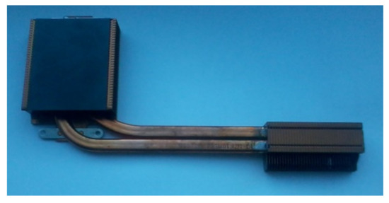
Figure 1.
Photo of the active heat sink.
The above-mentioned methods of cooling processors ensure effective heat dissipation. However, this is not enough in modern systems. High CPU load processing of large amounts of data requires the CPU to be equipped with appropriate algorithms to supervise its operation. One of the basic extensions is the integration of CPU and temperature sensor. It allows implementing advanced thermal load control procedures. The CPU load depends on its temperature. Such solutions (measuring the temperature of the semiconductor structure in real time) are often used [7,8]. Using the sensors appropriate algorithms can be implemented to control CPU performance. It is known as Dynamic Thermal Management (DTM). It is a set of techniques that controls the processor temperature and prevents it from overheating; e.g., reducing of the CPU clocking (DFS—Dynamic Frequency Scaling) or supplying voltage (DVS—Dynamic Voltage Scaling) leads to reduce CPU processing speed and to decrease its temperature [9,10,11,12,13]. DFS and DVS are based on CPU temperature monitoring using an integrated sensor. In general, the CPU load is determined by the current demand reported by the operating system. However, the efficiency is reduced if there is a risk of overheating. Consequently, the temperature decreases.
In the DTM method the key CPU temperatures are defined [9]: the allowable temperature limit value (Tmax), the first limit temperature value (Tthr1), the second limit temperature value (Tthr2) and the hypothetical limit temperature value (Tcoerce). They meet the dependence Tmax > Tthr1 > Tthr2 > Tcoerce. The CPU works normally when its temperature is lower than Tthr2. When it exceeds this value, the oscillator output frequency or supply voltage is reduced. The processor slows down and its temperature decreases. The algorithm allows for the efficiency increase when the internal temperature of the CPU drops below Tthr1. Of course, in the DTM method it is crucial to determine Tthr1 and Tthr2 temperatures properly in order not to overheat the CPU.
One of the modern approaches is not only the CPU temperature control, but also monitoring of the thermal conditions in CPU surroundings [14]. These conditions influence the CPU temperature. For example, there is a laptop in a room. Its processor is under heavy load. If the temperature in the room drops (e.g., in consequence of opening a window), the temperature of the heat sink block in contact with the environment drops first (right side in Figure 1). Then the temperature of the heat sink block in contact with the CPU drops (left side in Figure 1). Only then the temperature change will be detected by the sensor integrated in the processor. The reaction time will depend on the heat flow speed in the system. The thermal response time of the system (Point Heating Time—PHT) is long due to the high thermal inertia of the processor-radiator system, including a large mass of copper blocks [10].
The proposed set-up will use an additional temperature difference sensor between the processor and the heat sink. It will monitor thermal changes in the laptop environment. Information about the external conditions’ changes will be delivered to the processor much faster. It allows to take appropriate actions in advance. It means that monitoring of the outside conditions helps to predict the thermal state of CPU in the near future. It permits to react faster to dynamic changes in the environment. It can be applied to optimize the CPU’s efficiency; e.g., the processing speed can be decreased when both—ambient and CPU temperatures increase. An example of the introduced algorithm is TΔT power control method described in the literature [14]. Two temperature sensors are used in the method. One is integrated inside CPU (standard in modern CPUs). The second one is mounted on the heat sink, near the device housing. The second sensor monitors the ambient temperature and the CPU cooling conditions. The information about the temperature difference between CPU and its surroundings is obtained (TΔT). The results presented in the paper are related to TΔT power control method.
In this work a new temperature difference sensor for the TΔT system was developed to gain information for DTM algorithm. The requirement for the sensor was to monitor the temperature difference between the heat sink area near the processor and the heat sink area in contact with the environment (e.g., with air outside the laptop case—copper blocks, shown in Figure 1). It was decided to use a thermocouple-based device.
The thermocouple is a simple device based on the Seebeck phenomenon. It consists of two different conductive or semiconductive materials connected by opposite ends, e.g., as shown in Figure 2. An electromotive force will appear between the junctions when they are held at different temperatures and an electric current will flow in the system [3]. The value of the resulting electromotive force is directly proportional to the temperature difference between the junctions and to the parameters characterizing thermoelectric materials, Seebeck coefficients (Equation (1)).
where: α1, α2—Seebeck coefficients of materials A and B; THOT, TCOLD—temperatures of hot and cold thermoelectric junctions, respectively.
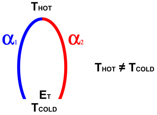
Figure 2.
Simple thermocouple—red and blue mark different materials.
The junction placed at a higher temperature is usually called “hot”. The junction placed in the lower one is called “cold”. Seebeck coefficients for conductive materials are in the range from several to a few tens of μV/K, for semiconductors—few hundreds of μV/K.
The wire thermocouples are the most frequently used in metrology. However, it is possible to fabricate thermocouples in the form of a planar structure applied on a flat, thin dielectric substrate, e.g., using screen-printing or magnetron sputtering methods [15,16,17,18,19]. Several, several dozen or even several hundred thermocouples can be integrated on one substrate, forming a thermopile. Thermopile is a set of thermocouples connected electrically in series and thermally in parallel. In this way the electrical signal generated by the device is multiplied. If the thermopile consists of n identical thermocouples, its output voltage will be n times higher. Such devices are used, e.g., to generate “green” energy for microelectronics [20,21,22]. They can be used also to build a temperature difference sensor.
Different dielectric materials can be used as a substrate for planar thermocouples. Rigid materials such as alumina or glass are used, as well as flexible materials such as polyimide or polyester foils. However, if the thermocouples are fabricated in the thick-film technology, using the screen-printing method, it is necessary to use a substrate appropriate to the temperatures used in the technological process (850 °C in standard). The Low Temperature Cofired Ceramic (LTCC) gives great opportunity [23]. It is a ceramic material supplied in the form of a thin, flexible tape. It can be freely formed in the planar plane—it can be cut, holes and channels can be made [24,25]. Single tapes can be folded in multilayers, creating three-dimensional (3D) structures with conductive paths buried inside [20,23,24,25]. During firing in a suitable time-temperature profile, the organic phase of the LTCC tape is removed. Ceramic grains are sintered. Consequently, a ceramic substrate similar in composition to alumina is obtained. Thanks to this technique it is possible to produce a ceramic substrate with a specific shape and to integrate elements such as conductive paths, via holes, contact pads, etc. into it.
2. Materials and Methods
2.1. Temperature Difference Sensor
Fabrication and tests of a sensor dedicated to typical passive radiators were presented in our previous paper [26]. In this work the research is focused on active heat sinks often used in laptops. Exemplary one is presented in Figure 1 and Figure 3. It is in fact the entire active cooling system containing:
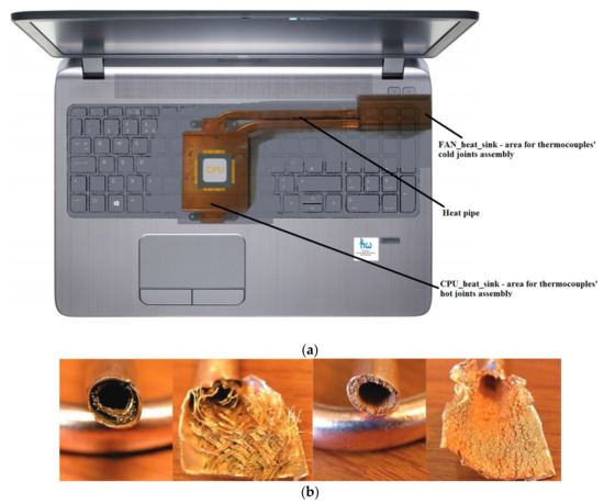
Figure 3.
Active heat sink: (a) location in the laptop; (b) examples of cross-sections of different heat pipes [27].
The CPU is located on the CPU_heat_sink, visible in the center of Figure 3a. The task of the copper block is to draw heat from the chip and transfer it to the heat pipe. Heat pipe is made usually as a copper tube containing porous material inside (Figure 3b), which is to facilitate the penetration of liquid from one end to the other (by gravity or capillary forces). The tube is filled with liquid (e.g., liquefied ammonia, acetone, ether or water), which evaporates near the CPU_heat_sink and draws heat from it. Then it liquefies on the colder part of the tube near FAN_heat_sink. This heat sink is located on the edge of the laptop case, so the external air can flow through it. The cooling efficiency can be increased by the fan.
The designed sensor should monitor the temperature difference between two spots on the heat sink (Figure 3a):
- Near the processor (on CPU_heat_sink);
- Near the cooling fan (on FAN_heat_sink).
The use of a sensor based on thermocouples enables direct monitoring of the temperature difference. The “hot” junctions of the thermocouple should be placed near the CPU (on CPU_heat_sink), while the “cold” one near the cooling fan (on FAN_heat_sink)—Figure 3a. The specificity of the active heat sink makes it impossible to produce a planar thermopile on a single rigid substrate and place it on the heat sink surface (because of its too complicated shape). The best solution for such a shape of heat sink seems to be the use of thick- or thin-film Resistance Temperature Detectors (RTD), thermistors or wire thermocouple. Two RTD, two thermistors or one thermocouple can be used to monitor the temperature difference between 2 points. In the case of RTDs or thermistors, each time one should look for the two most similar ones—characterized by the same response in the whole used temperature range. This is troublesome. In case of a thermocouple, this problem does not occur. Thermoelectric measurements are therefore a very simple way to determine the temperature difference between the two blocks. However, they have also some disadvantages. The first one is the very low output signal of a single wire thermocouple—on the level of several tens of μV/K. The second is the poor thermal contact between the measuring junction and the copper blocks’ surface—schematically it is shown in Figure 4a. Measuring junction in the form of weld of two wires (thermocouple legs) has the spherical shape that makes difficult heat flow from heat sink block to the thermocouple. The weld area exposed to convective cooling by the surrounding air is incomparably larger than the contact area with the copper block (Figure 4a). This introduces significant temperature measurement inaccuracies.
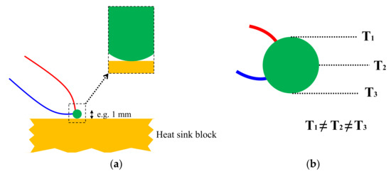
Figure 4.
Thermoelectric junction: (a) wire thermocouple on the copper heat sink and zoom of the heat sink/weld contact area; (b) temperature distribution in the volume of a large thermoelectric junction.
Moreover, the large volume of the weld and its exposure to convective cooling results in a nonuniform temperature distribution in the junction area (Figure 4b). The temperature gradient appears inside the junction. Together with the small temperature differences between the CPU_heat_sink and FAN_heat_sink blocks it can significantly influence the results.
The problem with the poor thermal contact can be partially solved by making a weld directly on the heat sink surface. A permanent connection between the thermocouple legs and the copper block is created. It improves the thermal contact. However, the volume of the thermoelectric junction still is too large (Figure 5). Moreover, the problem of a small output signal remains unsolved. This can be solved by using a thermopile. An exemplary solution is presented in Figure 6. However, a new problem with electrical contact appears. A short circuit occurs if the welds are in direct contact with the conductive copper block and it is impossible to read the output signal. Therefore, the thermocouple junctions have to be electrically separated from the copper surface. This can be achieved, e.g., by passivating the copper surface or by placing a thin insulating material on it (in Figure 6 the insulating layer is marked black). However, it is not possible to make a weld integrated with the copper surface, as shown in Figure 5. Consequently, the problem of large volume of the thermoelectric junction is renewed. All indicated problems and phenomena concern both ends of thermocouples and both types of thermoelectric junctions (“hot” and “cold” ones) placed on both copper blocks (CPU_heat_sink and FAN_heat_sink) visible in Figure 1 and Figure 3a.
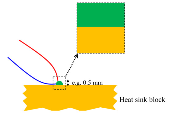
Figure 5.
Thermocouple junction integrated with the surface of the copper block.
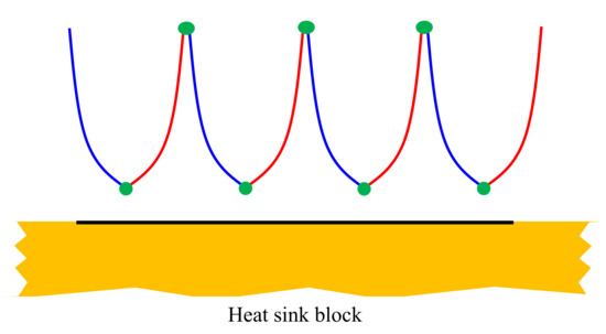
Figure 6.
Thermopile consisting of 4 thermocouples—application on a copper block.
It was decided to use a hybrid technique (Figure 7a), combining the advantages of film and wire thermocouples. The legs of thick-film thermocouples were screen-printed on a thin ceramic substrate. Such substrates were placed on both copper heat sink blocks (Figure 7b). Screen-printed legs were connected by thermoelectric wires. This made possible to connect thick-film thermoelectric junctions, which are located on separate and distant substrates. In such a solution, the thickness of the thermoelectric junction is only several µm, so it is many times smaller than in the case of wire thermocouples. The contact surface of the thin ceramic substrate with the heat sink is very large, which makes negligible temperature difference between these two volumes. The wire connection between the ceramic substrates allows to transmit the measurement signal in a simple way, despite the complex surface of the heat sink (Figure 1 and Figure 3a). Moreover, the fabrication of thermopile containing several thermocouples is not a big technological challenge and can be simply realized. It also should be noted that printed thermoelectric junctions are far away from the wires in this solution. This eliminates possible temperature disturbances resulting from the high thermal conductivity of the thermoelectric wires, whose diameter is large in comparison with the thickness of screen-printed thermocouples.
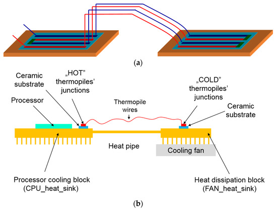
Figure 7.
Hybrid thermopile: (a) thermocouples printed on ceramic substrates, connected by thermoelectric wires; (b) schematic diagram of the hybrid wire/thick-film thermopile.
To sum up, Figure 7 shows the concept of the sensor to measure the temperature difference between two copper blocks of the active heat sink. Such a sensor is capable to detect thermal changes in the environment of the processor system (e.g., computer) and transmit information about them to the algorithm supervising the CPU operation. The sensor consists of several thermocouples forming a thermopile. However, they are not performed in a standard way (on a single substrate). The innovation of the solution is to split them into two separate substrates, connected by wires. All “hot” junctions are located on one substrate and all “cold” junctions on the second one. Thermocouples’ fabrication in the form of thick-film paths deposited on thin, flat ceramics results in a good thermal contact between the sensor and the heat sink. Due to the connection of the substrates using flexible thermoelectric wires of any length the complicated shape of the active heat sink (as shown in Figure 1) is not a problem. The sensor’s task is to detect thermal changes in the environment of the processor device. The “hot” junctions are located near the CPU (its temperature is controlled by a factory-integrated temperature sensor), on the CPU_heat_sink block. The “cold” ones are located at the other end of the active heat sink, on the FAN_heat_sink block, i.e., near the airhole in the device casing. Thermal changes in the environment affect the temperature of “cold” junctions. This can be detected immediately by the algorithm controlling the CPU as a change of thermoelectric voltage at the sensor output. This information can be used to modulate the CPU load (e.g., by TΔT power control method [13,14]).
2.2. Sensor Design
The sensor design assumes that a mosaic of paths will be screen-printed on two separated ceramic substrates, as is shown in Figure 8. The area visible on the right side of the picture is the substrate for FAN_heat_sink with “cold” thermocouples’ legs (two different thermoelectric materials marked as blue and red). The black indicates contact pads (made of well solderable material) for thermoelectric wires and measuring probes. The substrate for CPU_heat_sink (“hot” thermocouple junctions) is designed similarly. It is visible on the left side of the picture. These two substrates are connected with wires, made of two different thermoelectric materials.
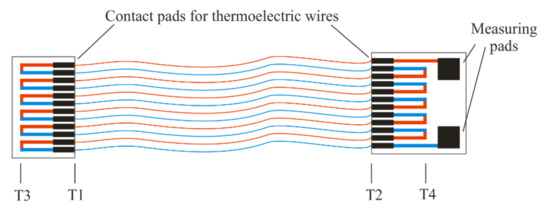
Figure 8.
Sensor design: two ceramic substrates with screen-printed thermocouples legs connected by thermoelectric wires.
The thermoelectric wires have to be made of the same material as the screen-printed paths. That is, legs screen-printed using material A on both substrates have to be connected with a wire made of material A. Similarly for the B tracks. If the wires have a different Seebeck coefficient than the screen-printed legs, the sensor will not function properly, according to the Law of Intermediate Materials. Instead of measuring temperature differences T3 − T4 (see Figure 8) it will measure T3 − T1 or T2 − T4. In an ideal situation T3 = T1 and T2 = T4, so the sensor output signal should be zero, theoretically. In a real system, the temperatures may vary slightly, which will generate a non-zero output signal.
An experiment was performed to verify above. Two sensors were fabricated according to Figure 8. Thermoelectric legs of Ag (red) and Ni (blue) inks were screen-printed on the substrates. They formed 6 Ag/Ni thermocouples. The Seebeck coefficient of each thermocouple was 21 µV/K, the thermoelectric force generated by each structure was 6 × 21 = 126 µV/K. The sensors differed in the thermoelectric wires used. In the first one (TST_Ag) only silver wires were used (Figure 9a). In the second one (TST_AgNi), silver and nickel wires were used (Figure 9b), red and blue in Figure 8, respectively. “Hot” sides (substrates) of the sensors were placed on a regulated heater, “cold” on a heat sink. “Hot” ones were heated from room temperature to 70 °C, while the temperature of the cold ones was stabilized (~21 °C). The output voltage of the structures was measured every 1 s. Figure 9 shows the structures and the obtained results.
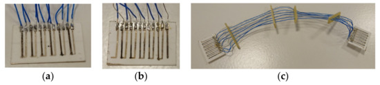
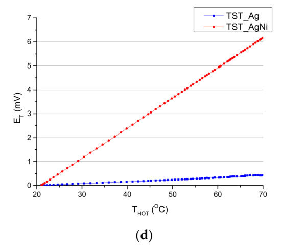
Figure 9.
Sensor prototypes: (a) TST_Ag fabricated using only silver wires (zoom of “hot” substrate); (b) TST_AgNi fabricated using silver and nickel wires (zoom of “cold” substrate); (c) TST_AgNi—the whole sensor; (d) output signal of TST_Ag and TST_Ni vs. temperature of “hot” junctions.
The highest voltage measured at the output of the TST_AgNi structure was 6 mV. It corresponds to the temperature difference dT = 48 °C. At the same time, the voltage at the output of TST_Ag was 0.43 mV, it corresponds to dT = 3.5 °C.
The voltage at the output of the TST_Ag sensor should be zero, theoretically. The difference is due to the fact that the thermoelectric wires take heat away from the T1 points lowering their temperature (see Figure 8). Consequently, the temperatures of T3 and T1 are not equal, resulting in a small electromotive force between these points. Analogously between T2 and T4.
The experimental results prove that it is not possible to make the described sensor using wires of a single material. It is necessary to use two different wires whose Seebeck coefficients will match the screen-printed legs. This is due to the Law of Intermediate Materials.
Three sensor versions have been designed and fabricated. They differ in thermoelectric materials.
2.2.1. Version A
The red and blue paths on both substrates as well as the contact pads (black) are made using the same material, PdAg-based ink. In fact, they are only electrical connectors, not thermocouple legs. The screen-printed paths have only a connecting function and according to the thermoelectric Law of Intermediate Materials do not affect the generated thermoelectric force. This law says that if the third (and subsequent) material is included in the thermoelectric circuit, it does not make any modifications to the measuring signal provided that both its ends are placed at the same temperature [3]. This is maintained for the considered device. The disadvantage of the solution is that the thermocouples monitor the temperature at the point of soldering the wires to the paths (in the area of contact pads). In other words, the temperature at the point of contact between thermoelectric wires and contact pads is monitored (points marked T1 and T2 in Figure 8). This is important because the cross-section of thermoelectric wires is much larger than the cross-section of screen-printed paths. Thus, they can draw the heat from the measuring points and reduce the measured temperature difference. It can be argued that the temperature difference T1 − T2 will be less than T3 − T4. Verification of this thesis will be presented in the paper later. The advantage of this solution is a simple construction. By transferring the thermoelectric junction from the weld (whose shape is poorly matched to the surface of the heat sink, Figure 4) to the flat ceramic substrate, good thermal contact is obtained. Nickel and silver thermoelectric wires were used for this version of sensor. Thus, the Ag/Ni thermocouple was formed. Contact pads in all sensor versions were made of well solderable PdAg ink (which, according to the Law of Intermediate Materials, did not affect the measurement results), which made it easier to solder of thermoelectric wires.
This sensor was fabricated in two variants: using PdAg-based ink (sensor marked A) or Ag-based ink (sensor marked A2) to investigate the influence of different materials on thermoelectric properties.
2.2.2. Version N
This variant eliminates the heat flow problems described above. The red paths on ceramic substrates were screen-printed using silver-based ink, the blue ones—using nickel-based ink. The thermoelectric junctions distanced from contact pads and thermoelectric wires. They are located at the points marked T3 and T4 in Figure 8. It was expected that the measured temperature difference will be higher than in version A. The aim of the research was to check if this difference is significant enough to compensate for the larger effort required for fabrication version N. The nickel and silver thermoelectric wires were used, similarly as in version A. The materials of the wires were matched to the screen-printed paths material. The Ag/Ni thermocouples were formed.
2.2.3. Version E
Both types of paths (red and blue) on the ceramic substrates were made using one material (Ag), similarly as in variant A. The difference was in the use of other thermoelectric wires. NiCr and CuNi wires were used. Thermocouples type E were formed. According to the literature, this combination generates thermoelectric voltage of 68 µV/K [3]. It is significantly more than for Ag/Ni combination, which generates 21 µV/K [15,20]. The aim of the research was to check whether the sensor of a simpler design but composed of more effective materials (in comparison with the N variant) would work better in practice. The electrical resistivity of NiCr as well as CuNi wires is significantly higher than Ni (0.07 Ω·µm) or Ag (0.016 Ω·µm) ones. Moreover, it depends on the exact content of Ni, Cr and Cu. In the research the wires with atomic percentage ratio 80:20 (NiCr) and 56:44 (Cu:Ni) were used. The electrical resistivities were 1.08 Ω·µm and 0.48 Ω·µm, respectively.
2.3. Sensor Fabrication
Legs of the miniature thermocouples were screen-printed on a single substrate of DP951 green tape (DuPont, USA, thickness 165 µm before firing). The paths were screen-printed using one or two different inks, depending on the sensor variant. In variant A it was PdAg-based DP6146 ink (DuPont, Wilmington, DE, USA, Figure 10a). In variant E it was Ag-based DP6145 ink (Figure 10a). In variant N the paths were made using DP6145 (DuPont, Wilmington, DE, USA, Ag-based) and ESL2554-N-1 (Ferro, Mayfield Heights, OH, USA, Ni-based) inks—Figure 10b. All paths were ended with contact pads of well solderable ink (black color in Figure 10). Aurel VS 1520A screen-printer was used.
Figure 10.
Thermopiles path mosaics: (a) for version A and E; (b) for version N.
The path mosaics on FAN_heat_sink are slightly different from those on CPU_heat_sink, as is shown in Figure 10. The former are equipped with additional contact pads to connect the measuring system. In both cases, the thermocouples legs were 5 mm in length, 300 μm in width and the spacing between the adjacent paths was 300 μm. The size of the contact pads was 2 × 0.45 mm2. The thickness of all printed films was about 15 μm—typical for screen-printing. Total area of the structure for CPU_heat_sink was 8 × 6 mm2 (before firing). Structures for FAN_heat_sink included additional 2 × 2 mm2 contact pads, which required the substrate to be increased to 9 × 9 mm2 (before firing).
Figure 11 shows a scheme of the sensor structure. It consisted of 5 DP951 tapes. On the 165 μm thick base layer (Figure 11a), the above-described paths (thermocouple legs) and contact pads were screen-printed (Figure 11b). The mosaic of paths was covered with three DP951 tapes (Figure 11c), forming a buried structure. Previously, using the laser cutting technique (LPKF ProtoLaser U laser system), holes were made in DP951 to make access to contact and measuring pads. These layers stiffen and strengthen the structure mechanically and create channels in which thermoelectric wires are mounted. The last tape (Figure 11d) covers the whole. Figure 12 shows, among others, a photo of the front of the structure with visible holes.
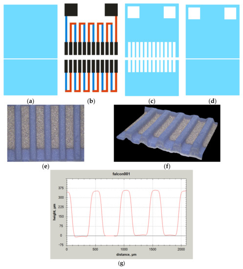
Figure 11.
Schematic and profile cut on sensor structure: (a) the base tape; (b) the thermocouples legs; (c) laser cut tapes (three tapes); (d) the cover tape; (e,f) 3-D photo of the structure without the cover tape; (g) profile of the structure without the cover tape.
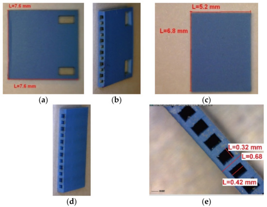
Figure 12.
LTCC based structures with buried thermoelectric paths: (a,b) the structure for FAN_heat_sink; (c,d) the structure for CPU_heat_sink; (e) holes for thermoelectric wires mounting.
Figure 11e,f show pictures of the area of contact pads after assembling the 4 lower tapes (without cover tape). The photos were taken using the Leica DM 2700M (Leica Camera AG, Wetzlar, Germany) optical microscope. Figure 11g shows the profile of the structure cross-section.
After assembling all tapes, the structures were laminated in an isostatic press, at the pressure of ~10 MPa. Then, the whole structure was fired in a suitable time-temperature profile at a peak firing temperature of 850 °C. DP951 tape shrinks about 13% in the X and Y axes and about 15% in the Z axis during firing. Finally, the planar dimensions of the structures were about 7.6 × 7.6 mm2 (LTCC on FAN_heat_sink—Figure 12a,b) and 6.8 × 5.2 mm2 (LTCC on CPU_heat_sink—Figure 12c,d). The thickness of the whole structure after firing was about 680 μm. Dimensions of mounting holes were about 420 × 320 μm2 (Figure 12e). The thermoelectric wires of 250 or 260 µm diameter (depending on the type) were installed in the holes in the further stages.
The solder material and the thermocouple wires were placed in the mounting holes in the next step. Then the whole structure was heated up to 300 °C. This temperature is not harmful for LTCC ceramics, but it melts the solder. The contact pads and thermoelectric wires are wetted. After cooling down, the final sensor structures were obtained. Figure 13 shows the final structures for FAN_heat_sink (a,c) and CPU_heat_sink (b) with mounted thermoelectric wires. The whole sensor is presented in Figure 13d where both LTCC structures, thermoelectric wires as well as two measurement wires are visible. The basic electrical and thermoelectric parameters of the fabricated sensors were measured—internal electrical resistance as well as Seebeck coefficient. The automatic measuring system was used [15,17,20]. Table 1 presents the basic information about the sensors.
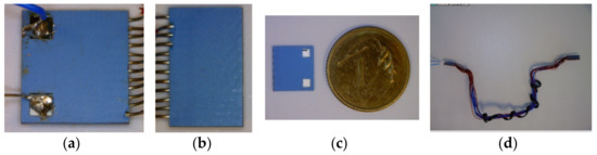
Figure 13.
The final structure: (a,c) LTCC substrate for FAN_heat_sink; (b) LTCC substrate for CPU_heat_sink; (d) thermoelectric temperature difference sensor.

Table 1.
Basic parameters of fabricated and investigated thermoelectric sensors.
3. Results
Sensor A was fabricated in two variants. In the first (marked A), the screen-printed legs were made from PdAg-based DP6146 ink (approximately 75% Ag). In the second variant (marked A2) from DP6145R ink, based on Ag. The other details were identical. A comparative study between the two was performed to see if the type of material used to screen-print the legs made a difference in sensor performance. The “hot” junctions were assembled near the CPU (CPU_heat_sink in Figure 3a and Figure 7b) on the copper block of the active heat sink. The “cold” junctions—on the copper block for heat dissipation (FAN_heat_sink). A thin alumina substrate with four thick-film resistors that simulated four processor cores was used as the CPU thermal model [29,30]. The results are presented in Figure 14.
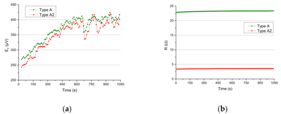
Figure 14.
The comparative study between sensors A and A2—different material for screen-printed legs: (a) output voltage responses vs. time; (b) internal resistance vs. time.
The tested structures differed significantly in internal resistance. This is directly due to the ink resistivity, which is several times higher for PdAg. However, the most important parameter is the voltage signal of the sensor. It was at a comparable level for both tested structures. The sensor output signal of type A is on average ~4% higher than that of type A2. This small difference may be due to the thermal conductivity of the materials, which is significantly higher for the silver-based ink. Consequently, somewhat larger temperature gradient may occur between the thermoelectric junctions of the A structure than in the A2 structure. Since the difference between the A and A2 sensor is small, the A sensor was chosen for further study.
To measure the variants A, N and E of the sensor at the same time, they were placed next to each other on the processor model (directly on the heater)—Figure 15. Figure 15a shows the location of the structure with “hot” thermocouple junction on the CPU_heat_sink. Three sensors are visible, from left to right variants N, E and A, respectively. The sensors were pressed down using the test needles to improve thermal contact with the heater surface. Figure 15b shows the location of the structure with “cold” thermocouple junction on FAN_heat_sink.
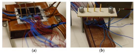
Figure 15.
Sensor structures on the copper heat sink blocks: (a) the „hot” thermoelectric junctions on CPU_heat_sink; (b) the „cold” thermoelectric junctions on FAN_heat_sink.
After the sensors were placed on the active heat sink, measurements were started to compare all sensors. The processor model was heated up by connecting 12 V and 0.2 A to each of the resistors. Total power delivered to the heater (CPU_heat_sink) was equal to 9.6 W. The temperature of CPU_heat_sink and FAN_heat_sink was monitored by pyrometers. Internal resistance and voltage response of each sensor was measured. The sensors’ responses to changes in cooling conditions of the “cold” block (FAN_heat_sink) were investigated. For this purpose, the measuring set-up was equipped with a 12 V cooling fan, which was cyclically switched on and off. In this way the cooling conditions of the FAN_heat_sink block were changed. Information about changes in thermal conditions should be used by the algorithm controlling the processor. It is important to achieve the information as soon as possible. It should be kept in mind that the typical 4 GHz processor can perform up to 4 × 10⁹ operations per second, so time is essential. All data were cyclically read and recorded by 34970A Data Logger (Keysight Technologies, Santa Rosa, CA, USA).
3.1. Experiment 1
In the first experiment power was delivered to the heater (CPU thermal model). As it was heated up the voltage responses of each sensor and its internal resistance were measured every 10 s. The entire test lasted about 3000 s. All sensors were measured simultaneously under identical conditions, allowing direct comparison. The results are shown in Figure 16. An efficient active heat sink causes that the temperature difference between the “hot” Cu block (CPU_heat_sink) and “cold” one (FAN_heat_sink) is small. During all experiments, the temperature of both blocks varied from 50 °C to 64 °C and the temperature difference ΔT was established just after a few dozen seconds. The electrical responses of the sensors were stabilized at specific levels:
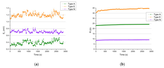
Figure 16.
Sensors A, E and N characteristics during warming up the heater: (a) output voltage responses vs. time; (b) internal resistance vs. time.
- About 0.4 mV for version A.
- About 1.2 mV for version E.
- About 0.7 mV for version N.
This means, according to Equation (1), the sensor N measured ΔT of about 5.5 °C, while sensors A and E—about 3 °C. This shows the influence of sensor design on the measurement results. In versions A and E the thermoelectric junctions are located at the soldering points of the thermoelectric wires (points T1 and T2 in Figure 8). In version N they are distanced from the wires (points T3 and T4 in Figure 8). Consequently, the sensitivity of the sensor N is almost twice higher.
It can be explained by the fact that thermoelectric wires are located in the air (Figure 8) near at room temperature. The air cools the wires down. This affects the temperature of the place where the wires are connected to the LTCC substrate—it is locally lower in relation to the rest of the LTCC substrate. If the thermoelectric junction is located there, its temperature is also lower. This is the case with versions A and E of the sensor (Figure 8, Figure 10a). In the version N, the thermoelectric junctions are distanced from the soldering point (Figure 8 and Figure 10b). Its influence on temperature is much smaller consequently. Note that the wires are relatively thick (250–260 µm) compared to the whole sensor (680 µm) and the screen-printed legs (15 µm). They have also a significantly higher thermal conductivity—12–429 W/m∙K for wires (see Table 1) compared to about 3 W/m∙K for LTCC.
The results of the experiment confirm the thesis presented in Section 2.2.1—the temperature difference between points T1 − T2 was lower than between T3 − T4 ones (Figure 8). Distancing the thermoelectric junctions from the wires has a significant impact on sensitivity. The internal resistance of the sensors increases slightly as the heater warms up (Figure 16b) because all used conductors were characterized by the positive temperature coefficient of resistance (TCR). The TCR is about 5900 ppm/K for Ni, 3800 ppm/K for Ag. The TCR for CuNi as well as NiCr depends on the atomic percentage ratio [31]. It is about 30 ppm/K for used CuNi (Cu56Ni44) and 150 ppm/K for NiCr (Ni80Cr20). However, the temperature during all investigations remained between 23 °C and 62 °C, so the resistance changes were only slight.
To verify the results, numerical simulations were performed in COMSOL Multiphysics 5.3 (Comsol, Burlington, MA, USA). A simplified model was built, which corresponds to the tested sensor and the conditions of the tests. It consisted of two LTCC substrates with dimensions of 5.2 × 6.8 × 0.68 mm3, with buried Ag and Ni legs (5000 × 300 × 15 µm3). The substrates were connected by 160 mm long Ag and Ni wires with a diameter of 250 µm. The wires were mounted in LTCC substrates at a length of 2 mm. Typical physical parameters for LTCC, Ni and Ag (shown in Table 1) were used as input data for the simulation. The ambient temperature was set at 20 °C. The system was heated with a 9.6 W heater. Free convection conditions were selected, the characteristic length was calculated as area/perimeter.
The simulation results are shown in Figure 17. Figure 17a shows a general view of the sensor. The LTCC substrate for CPU_heat_sink is on the left side. In Figure 17b the sensor was cut by the plane passing through the center of the screen-printed legs (in Z axis). The temperature difference between LTCC substrates as well as between the points marked as T1 − T4 in Figure 8 can be seen. Exact values can be read from the line graphs in Figure 17c. The blue line indicates the LTCC substrate for CPU_heat_sink, green for FAN_heat_sink. These are the temperature distribution along the printed legs from Figure 17b—the exact line for CPU_heat_sink (blue) is shown in Figure 17d. According to the simulation results, the temperatures in T1-T4 points (see Figure 8) are:
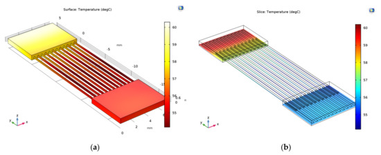
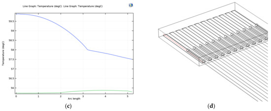
Figure 17.
Simulation results of temperature distribution along thermoelectric legs: (a) general view of the sensor; (b) cross-section of the thermoelectric legs; (c) temperature distribution along screen-printed legs inside of left (blue) and right (green) LTCC substrates; (d) visualization of the line for blue graph.
- 57.5 °C for T1.
- 55.5 °C for T2.
- 60.0 °C for T3.
- 55.8 °C for T4.
According to the simulation results, the temperature difference sensors should indicate:
- 2 °C—sensors A and E.
- 4.3 °C—sensor N.
These simulations are for a simplified model. However, results show the same trend as the measurement results and similar values. This confirms that the temperatures at points T1-T4 may be different, as the experimental results show. This allows to conclude that the geometric arrangement used in the N-type sensor is more effective than that used in the A-, A2- and E-type sensors.
3.2. Experiment 2
The purpose of the second experiment was to investigate the response of the sensors to changes in the ambient conditions of the system. Changes in the voltage response of the sensors (signal level) and their response times were monitored. The thermal model of the processor was already heated up. Both CPU_heat_sink and FAN_heat_sink temperatures were stabilized. The fan was cyclically turned on and off, changing the thermal conditions of the FAN_heat_sink block. From a physical point of view, the forced convection coefficient was changed. All sensors were measured simultaneously under identical conditions, allowing direct comparison. Voltage responses of all three sensors were recorded every 1 s. The times of switching on/off the fan are presented in Table 2.
Table 2.
The times of switching on/off the fan in experiment 2.
The whole experiment lasted about 110 s. Figure 18 shows the responses of the sensors. The black dotted lines indicate the moments when the fan was switched on and off.
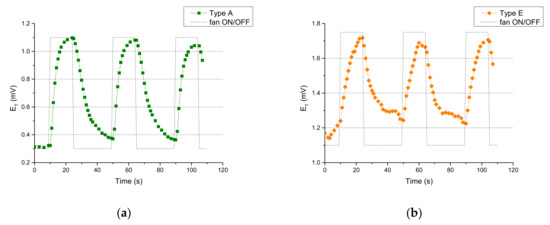
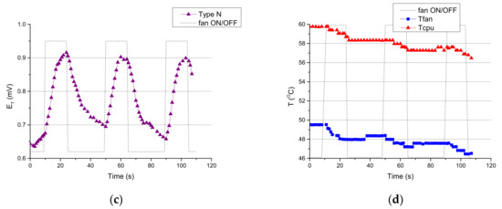
Figure 18.
The voltage response of the sensors—measurements every 1 s: (a) sensor version A; (b) sensor version E; (c) sensor version N; (d) the temperature of FAN_heat_sink block (blue) and CPU_heat_sink block (red)—pyrometer measurement. The black dotted line indicates the moments when the fan was switched on and off.
The responses of the sensors are almost instantaneous. After on/off the fan, the sensors’ reactions occur in the next measurement cycle. However, the interval of subsequent measurements is quite long—about 1 s. During this time the processor is able to perform many operations. Therefore, it was decided to conduct more detailed investigations (see Experiment 3).
The return time of the sensor output signal to the state before the change of cooling conditions is quite long. It can be estimated at over 30 s. However, this is not caused by the sensors themselves, but by the large heat capacity of the entire heat sink block.
The characteristics presented in Figure 18d shows the influence of cooling condition change on FAN_heat_sink and CPU_heat_sink blocks temperatures. Every switching on the fan causes the temperature drop. Any change of the FAN_heat_sink temperature affects the temperature difference between it and the CPU_heat_sink.
The maximum level of the voltage response of the sensor A was about 1.1 mV, E—1.7 mV, N—0.9 mV. The thermal conditions were equal for each sensor. The sensor version E generates the highest output signal, because it is fabricated using the most thermoelectrically efficient materials (CuNi/NiCr, E-type thermocouple). However, more important parameter is the range over which the output signal changes (ΔU = ETmax − ETmin). The range ΔU can be extracted from Figure 18 as 0.20–0.25 mV for sensor N, 0.45 mV for sensor E and 0.75 mV for sensor A. Sensor version A seems to have the highest sensitivity to thermal condition changes. It should be noted that the responses of sensors A and N differ from each other despite the fact that they were fabricated using the same thermoelectric wires.
3.3. Experiment 3
The third experiment was similar to the second one, but the measurement interval was reduced. The purpose was to investigate sensors response time with the accuracy better than in experiment 2. The thermal equivalent of the processor was already heated up. Both CPU_heat_sink and FAN_heat_sink temperatures were stabilized. The fan was cyclically turned on and off, changing the thermal conditions of the FAN_heat_sink block. The times of switching on/off the fan are presented in Table 3. The fan was switched on for 10 s each time. The interval between switch off and switch on was 10, 15 or 20 s.
Table 3.
The times of switching on/off the fan in experiment 3.
Both, the sensors voltage responses as well as the temperature of CPU_heat_sink and FAN_heat_sink blocks were investigated. The measurement interval was 0.209 s. This is the limit value for the used Keysight 34970A data logger. Between 650 and 800 measurements were taken for each sensor. Each sensor was measured individually, in a separate measurement cycle (it was necessary to obtain 0.209 s interval). Therefore, the thermal conditions were slightly different for each measurement. Figure 19 shows the results for sensors A, E and N.
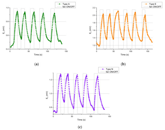
Figure 19.
The voltage response of the sensors—measurements interval 0.209 s: (a) sensor version A; (b) sensor version E; (c) sensor version N. The black dotted line indicates the moments when the fan was switched on and off.
Characteristics presented in Figure 19 show that the sensors responses are practically immediate. When the fan is turned on as well as it is turned off, the signal starts to change immediately. However, analysis of the subsequent measurement points revealed some differences between the sensors. The sensors increase the level of the generated signal in the first interval—i.e., the first measurement after switching the fan on/off shows a difference in the signal level. This is a slight difference, but it can be detected by the sensors used. For sensor N the change of the signal level by 1% occurs after approximately 0.2–0.4 s (first or second measurement cycle) after switching on/off the fan. On the other hand, the sensor E changes the signal level by 1% after 0.4–0.6 s when switching on and 0.4 s when switching off the fan whereas sensor A—0.4 s after switching on/off the fan.
4. Discussion and Conclusions
The paper presents the concept, fabrication and investigation of the hybrid thermoelectric sensor, which combines wire and thick-film thermocouples. Its task is to monitor the temperature difference at the opposite ends of the active heat sink, typically used in laptops.
Sensors were made by screen-printing of conductive inks on LTCC tapes. Every version of the sensor consists of two LTCC substrates (with printed paths) and thermoelectric wires. The LTCC substrates have direct contact with the copper blocks of the active heat sink, in the paper marked as CPU_heat_sink and FAN_heat_sink (Figure 3a and Figure 7b). This topology gives very good surface contact between the sensor and the active heat sink. Moreover, the measurement points (thermoelectric junctions) were distanced from the wires. Thanks to this, the negative influence of heat transport through the wires volume on the results was reduced.
The LTCC substrates are connected by thermoelectric wires, which allow the sensor to fit any shape of the active heat sink. This significantly simplifies the integration of the sensor with the heat sink. Three versions of the sensor, differing in the applied thermoelectric materials and the location of measuring junctions, were fabricated. They were marked A (or A2), E and N. Different thermoelectric materials determine the output signal level. The described investigations showed that all sensors fulfill the requirements and can be used for the assigned task. Sensor E has the highest electrical response. It uses CuNi and NiCr thermoelectric wires, forming a classical type E thermocouple. However, the signal from sensors A and N is also high enough for practical application.
The investigations shown that different locations of the thermoelectric junctions affect the sensor output signal. Thermoelectric wires have a large volume compared to screen-printed paths. The heat transport by them is therefore much higher. If the wires are close to the printed thermoelectric junctions (versions A, A2 and E of the sensor), they have a relatively strong influence on their temperature in comparison with sensor N, where the junctions are significantly distanced from the wires. This translates into several effects. Firstly, the temperature difference measured by the N sensor is about 80% higher than for sensors A and E (experiment 1, Figure 16). This is a big advantage. When sensors are fabricated using the same thermoelectric wires, this directly translates into their output voltage level. A comparison of sensors N and A shows that distancing the junctions from the wires increases the output electrical signal from 0.4 mV to 0.7 mV (Figure 16). The use of thermoelectric materials with better efficiency allows to obtain an even higher signal at the output. A comparison of sensors N and E shows that despite the short distance between the wires and the thermoelectric junctions, sensor E generates a signal of 1.2 mV, i.e., 70% higher than sensor N (Figure 16). This is due to the fact that Seebeck coefficient of CuNi/NiCr thermocouple is more than 3 times higher than for Ag/Ni combination (68 µV/K and 21 µV/K, respectively). However, in this case other advantages of the N-sensor are lost (described below).
The second effect of distancing the thermoelectric junctions from the wires is increasing the temperature difference between the measuring points (thermoelectric junctions). For sensors versions A and E ΔTA/E = T1 − T2 (see Figure 8), for version N ΔTN = T3 − T4. Results of the investigation show that ΔTA/E < ΔTN (experiment 1, Figure 16 and Figure 17). Consequently, the sensitivity of sensor N should be better than for versions A and E. However, the results obtained in experiment 2 do not support the above. The range ΔU over which the output signal changes is much wider for sensors A and E: about 0.25 mV for sensor N, 0.45 mV for sensor E and 0.75 mV for sensor A (Figure 18). Further extensive comparative studies of the presented sensors should analyze why such results were obtained. One possible explanation is the specific conditions of the experiments. The forced cooling of the FAN_heat_sink block was using a fan. The generated airflow affected not only the temperature of the FAN_heat_sink block, but also the temperature of the thermoelectric wires. Lowering their temperature may have affected the temperature of the “cold” thermoelectric junctions in sensors A and E (in sensor N as well, but with lower impact due to the larger distance from the wires). This improved the performance of sensors A and E relative to N. It can be hypothesized here that the N-type sensor is better suited for monitoring the temperature of the FAN_heat_sink block, while the A and N-type sensors are better suited for monitoring its environment. This should be verified by further research by adding an experiment where the fan is replaced by a water-cooling system, for example.
The third effect is an improvement of the sensor reaction time. The sensor N exhibits a slightly faster change of the output signal than versions A or E. The difference may result from the volume (heat capacity) of the thermoelectric junction—in versions A and E it is a solder joint with a large volume (see Figure 5). In version N the junction is much smaller (screen-printed legs, 15 µm in thick) and therefore its heat capacity is smaller. This may result in faster sensor response. The difference is noticeable but very small, the results were at the limit of the measuring performance of used instruments. The high-speed measurement system should be set up to better investigate this in future work. It should be noted that the reaction time is a second key parameter in the considered application of the sensor. In this context, the sensor N seems to be the optimal solution. This means that distancing the thermoelectric junctions from the wires is more important than the optimal choice of thermoelectric materials. The voltage response of all versions of the sensor is on a functional level.
The sensors are suitable for measuring the temperature difference in the proposed application, they can be used in further work on TΔT algorithms.
Author Contributions
Conceptualization, P.M.M. and M.G.; formal analysis, P.M.M. and A.D.; investigation, P.M.M. and M.G.; methodology, P.M.M.; supervision, A.D.; validation, P.M.M. and A.D.; visualization, P.M.M.; writing—original draft, P.M.M.; writing—review and editing, A.D. All authors have read and agreed to the published version of the manuscript.
Funding
This research was funded by the National Science Centre (grant number 2014/13/B/ST7/01634 (FALCON)) and statutory activity of the Wrocław University of Science and Technology.
Conflicts of Interest
The authors declare no conflict of interest. The funders had no role in the design of the study; in the collection, analyses or interpretation of data; in the writing of the manuscript, or in the decision to publish the results.
References
- Suleiman, D.; Amin, H.; Husein, T. Microprocessors fan speed control for dynamic thermal management. In Proceedings of the 4th WSEAS International Conference on Information Security, Communications and Computers, Tenerife, Spain, 16–18 December 2005; pp. 360–364. [Google Scholar]
- Cai, Y.; Liu, D.; Yang, J.-J.; Wang, Y.; Zhao, F.-Y. Optimization of Thermoelectric Cooling System for Application in CPU Cooler. Energy Procedia 2017, 105, 1644–1650. [Google Scholar] [CrossRef]
- Rowe, D.M. Thermoelectrics Handbook—Micro to Nano; CRC Press Taylor & Francis: Boca Raton, FL, USA, 2006. [Google Scholar]
- Escher, W.; Michel, B.; Poulikakos, D. A novel high performance, ultra thin heat sink for electronics. Int. J. Heat Fluid Flow 2010, 31, 586–598. [Google Scholar] [CrossRef]
- Siricharoenpanich, A.; Wiriyasart, S.; Srichat, A.; Naphon, P. Thermal management system of CPU cooling with a novel short heat pipe cooling system. Case Stud. Therm. Eng. 2019, 15, 100545. [Google Scholar] [CrossRef]
- Elnaggar, M.; Edwan, E. Chapter 4: Heat pipes for computer cooling applications. In Electronics Cooling; Sohel Murshed, S.M., Ed.; IntechOpen: Rijeka, Croatia, 2016; pp. 51–78. [Google Scholar]
- Intel® CoreTM i7-900. Desktop Processor Series on 32-nm Process. Available online: www.intel.com (accessed on 10 December 2019).
- AMD FX Processors Unleashed: A Guide to Performance Tuning with AMD Overdrive and the New AMD FX Processors. Available online: www.amd.com (accessed on 10 December 2019).
- Gołda, A.T.; Kos, A.J. Optimum control of microprocessor throughput under thermal and energy saving constraints. Microelectron. Reliab. 2013, 53, 582–591. [Google Scholar] [CrossRef]
- Mikula, S.; Kos, A. Thermal Dynamics of Multicore Integrated Systems. IEEE Trans. Compon. Packag. Technol. 2010, 33, 524–534. [Google Scholar] [CrossRef]
- Salami, B.; Noori, H.; Mehdipour, F.; Baharani, M. Physical-aware predictive dynamic thermal management of multi-core processors. J. Parallel Distrib. Comput. 2016, 95, 42–56. [Google Scholar] [CrossRef]
- Ayoub, R.; Rosing, T. Predict and act: Dynamic thermal management for multi-core processors. In Proceedings of the International Symposium on Low Power Electronics and Design, San Francisco, CA, USA, 19–21 August 2009; pp. 99–104. [Google Scholar]
- Kong, J.; Chung, S.W.; Skadron, K. Recent thermal management techniques for microprocessors. ACM Comput. Surv. 2012, 44, 1–42. [Google Scholar] [CrossRef]
- Kocanda, P.; Kos, A. Improvement of multicores throughput based on environmental conditions. Microelectron. Reliab. 2016, 60, 78–83. [Google Scholar] [CrossRef]
- Markowski, P.; Dziedzic, A. Planar and three-dimensional thick-film thermoelectric microgenerators. Microelectron. Reliab. 2008, 48, 890–896. [Google Scholar] [CrossRef]
- Kohl, M.; Veltl, G.; Busse, M. Printed Sensors Produced via Thick-film Technology for the Use in Monitoring Applications. Procedia Technol. 2014, 15, 107–113. [Google Scholar] [CrossRef]
- Gierczak, M.; Prażmowska-Czajka, J.; Dziedzic, A. Thermoelectric mixed thick-/thin film microgenerators based on con-stantan/silver. Materials 2018, 11, 9. [Google Scholar]
- Tang, Y.-Q.; Fang, W.-Z.; Lin, H.; Tao, W.-Q. Thin film thermocouple fabrication and its application for real-time tempera-ture measurement inside PEMFC. Int. J. Heat Mass Transf. 2019, 141, 1152–1158. [Google Scholar] [CrossRef]
- Nowak, D.; Turkiewicz, M.; Solnica, N. Thermoelectric properties of thin films of germanium-gold alloy obtained by mag-netron sputtering. Coatings 2019, 9, 120. [Google Scholar] [CrossRef]
- Markowski, P.M. Multilayer thick-film thermoelectric microgenerator based on LTCC technology. Microelectron. Int. 2016, 33, 155–161. [Google Scholar] [CrossRef]
- Kobayashi, A.; Konagaya, R.; Tanaka, S.; Takashiri, M. Optimized structure of tubular thermoelectric generators using n-type Bi2Te3 and p-type Sb2Te3 thin films on flexible substrate for energy harvesting. Sens. Actuators A Phys. 2020, 313, 112199. [Google Scholar] [CrossRef]
- Yang, S.; Cho, K.; Park, Y.; Kim, S. Bendable thermoelectric generators composed of p- and n-type silver chalcogenide na-noparticle thin films. Nano Energy 2018, 49, 333–337. [Google Scholar] [CrossRef]
- Sobocinski, M.; Putaala, J.; Jantunen, H. Chapter 6: Multilayer low-temperature co-fired ceramic systems incorporating a thick-film printing process. In Printed Films. Materials Science and Applications in Sensors, Electronics and Photonics; Pru-denziati, M., Hormadaly, J., Eds.; Woodhead Publishing Limited: Cambridge, UK, 2012; pp. 134–164. [Google Scholar]
- Dabrowski, A.; Rydygier, P.; Czok, M.; Golonka, L. High voltage applications of low temperature co-fired ceramics. Microelectron. Int. 2018, 35, 146–152. [Google Scholar] [CrossRef]
- Malecha, K.; Jasińska, L.; Grytsko, A.; Drzozga, K.; Słobodzian, P.; Cabaj, J. Monolithic Microwave-Microfluidic Sensors Made with Low Temperature Co-Fired Ceramic (LTCC) Technology. Sensors 2019, 19, 577. [Google Scholar] [CrossRef]
- Markowski, P.M.; Gierczak, M.; Dziedzic, A. Modelling of the Temperature Difference Sensors to Control the Temperature Distribution in Processor Heat Sink. Micromachines 2019, 10, 556. [Google Scholar] [CrossRef]
- Heat Pipe Wick Structures. Available online: http://www.frostytech.com (accessed on 14 February 2019).
- Incropera, F.P.; DeWitt, D.P. Fundamentals of Heat and Mass Transfer, 3rd ed.; Wiley&Sons, Inc.: Hoboken, NJ, USA, 1990. [Google Scholar]
- Markowski, P.; Gierczak, M.; Dziedzic, A. Testing of the thermal model of microprocessor. In Proceedings of the 2017 40th International Spring Seminar on Electronics Technology (ISSE), Sofia, Bulgaria, 10–14 May 2017; Institute of Electrical and Electronics Engineers (IEEE): Piscataway, NJ, USA, 2017; pp. 1–4. [Google Scholar]
- Gierczak, M.; Stojek, K.; Dziedzic, A. Temperature distribution on a quad-core microprocessor and quad-core microproces-sor/heat sink structure. Przegląd Elektrotechniczny 2017, 93, 210–213. [Google Scholar]
- Kim, Y.-J.; Lee, W.-B.; Choi, K.-K. Effect of seed layers and rapid thermal annealing on the temperature coefficient of resistance of Ni Cr thin films. Thin Solid Film. 2019, 675, 96–102. [Google Scholar] [CrossRef]


Publisher’s Note: MDPI stays neutral with regard to jurisdictional claims in published maps and institutional affiliations. |
© 2021 by the authors. Licensee MDPI, Basel, Switzerland. This article is an open access article distributed under the terms and conditions of the Creative Commons Attribution (CC BY) license (https://creativecommons.org/licenses/by/4.0/).