Article

Temperature Dependent Analytical Model for the Threshold Voltage of the SiC VJFET with a Lateral Asymmetric Channel

1
Microelectronics and Instrumentation Laboratory, University of Monastir, Avenue Taher Hadded B.P 56, Monastir 5000, Tunisia
2
Centre for Research on Microelectronics & Nanotechnology, Sousse Technology Park, BP 334 Sahloul, Sousse 4050, Tunisia
*
Author to whom correspondence should be addressed.
Electronics 2021, 10(12), 1494; https://doi.org/10.3390/electronics10121494
Submission received: 24 May 2021 / Revised: 10 June 2021 / Accepted: 17 June 2021 / Published: 21 June 2021

Abstract

:
The wide-bandgap (WBG) semiconductor devices for modern power electronics require intensive efforts for the analysis of the critical aspects of their operation. In recent years, silicon carbide (SiC) based field effect transistor have been extensively investigated. Motivated by the significant employment of the SiC Vertical Junction Field Effect transistors with lateral channel (LC-VJFET) in the development of high-voltage and high temperature applications, the properties of the LC-VJFET device are investigated in this work. The most important normally-ON LC-VJFET parameter is their threshold voltage (VTh), which is defined as the gate-to-source voltage necessary to block the device. The higher complexity of the blocking operation of the normally-ON device makes the accurate knowledge of the VTh as a fundamental issue. In this paper, a temperature dependent analytical model for the threshold voltage of the normally-ON LC-VJFET is developed. This analytical model is derived based on a numerical analysis of the electrical potential distribution along the asymmetrical lateral channel in the blocking operation. To validate our model, the analytical results are compared to 2D numerical simulations and experimental results for a wide temperature range.

1. Introduction

The threshold voltage (VTh) and its dependence on temperature is an important parameter of any FET structure for device evaluation and circuit design. Several works took place in the literature on its modeling for MOSFETs [1,2,3,4,5,6]. However, there is a lack of similar work for power JFETs structure. During the last decade, wide bandgap devices such as those made of silicon carbide (SiC), have emerged as promising power switching devices for a wide field of advanced electronic applications, especially at high temperature and high voltage. Some of them have been fabricated and tested in various research laboratories, and others are on the market [7,8,9,10,11,12,13,14,15]. Compared with the SiC MOSFET, SiC VJFET received a lot of attention because of its threshold voltage (Vth) stability for different temperature values, since no reliability issues appear with gate oxide on contrary to SiC MOSFETs [5,6,7]. Different structures of the SiC VJFET device have been developed and studied [16,17,18,19,20,21,22,23,24,25]. Among of them, in this paper, the SiC LC-VJFET of Figure 1 [16,20] is investigated under a physical model of the threshold voltage. The SiC LC-VJFET has a normally-on behavior. In other words, it conducts current even if no gate-source voltage is applied. To turn this JFET off, a negative gate-to-source voltage bias should be applied. The main parameter that controls the blockage of the device is the gate-to-source threshold voltage. The blocking condition of the device corresponds to a pinch-off operation where the saturation current reaches zero. Although this condition is very important for the analysis and the modeling of the device, few studies in this context have been published, generally leading to a complex or non-analytical expression of the threshold voltage [26,27].
In a previous work [26], the modeling of the asymmetrical double gate channel of the SiC LC-VJFET structure was investigated. A numerical method has been used to define the blocking conditions of the JFET device. These conditions have been presented by complex functions that are not easy to implement in software to simulate the physical model of the JFET. Therefore, for such complicated SiC LC-VJFET structure, it is a great interest to elaborate an analytical expression of the threshold voltage and its dependence with the temperature. Figure 1 represents the schematic of the investigated device LC-VJFET.
In the present study, an analytical model of threshold voltage for the SiC LC-VJFET is derived. We demonstrate that this model is far from being a classic threshold voltage expression [28]. We will show that the analytical expression of the threshold voltage is simple and easy to use. The proposed model can be used as an efficient tool for design, fabrication and modeling for the SiC VJFET device. The validity of the developed analytical model is investigated by comparing the model results with the experimental and the numerical simulation results within a wide temperature range.

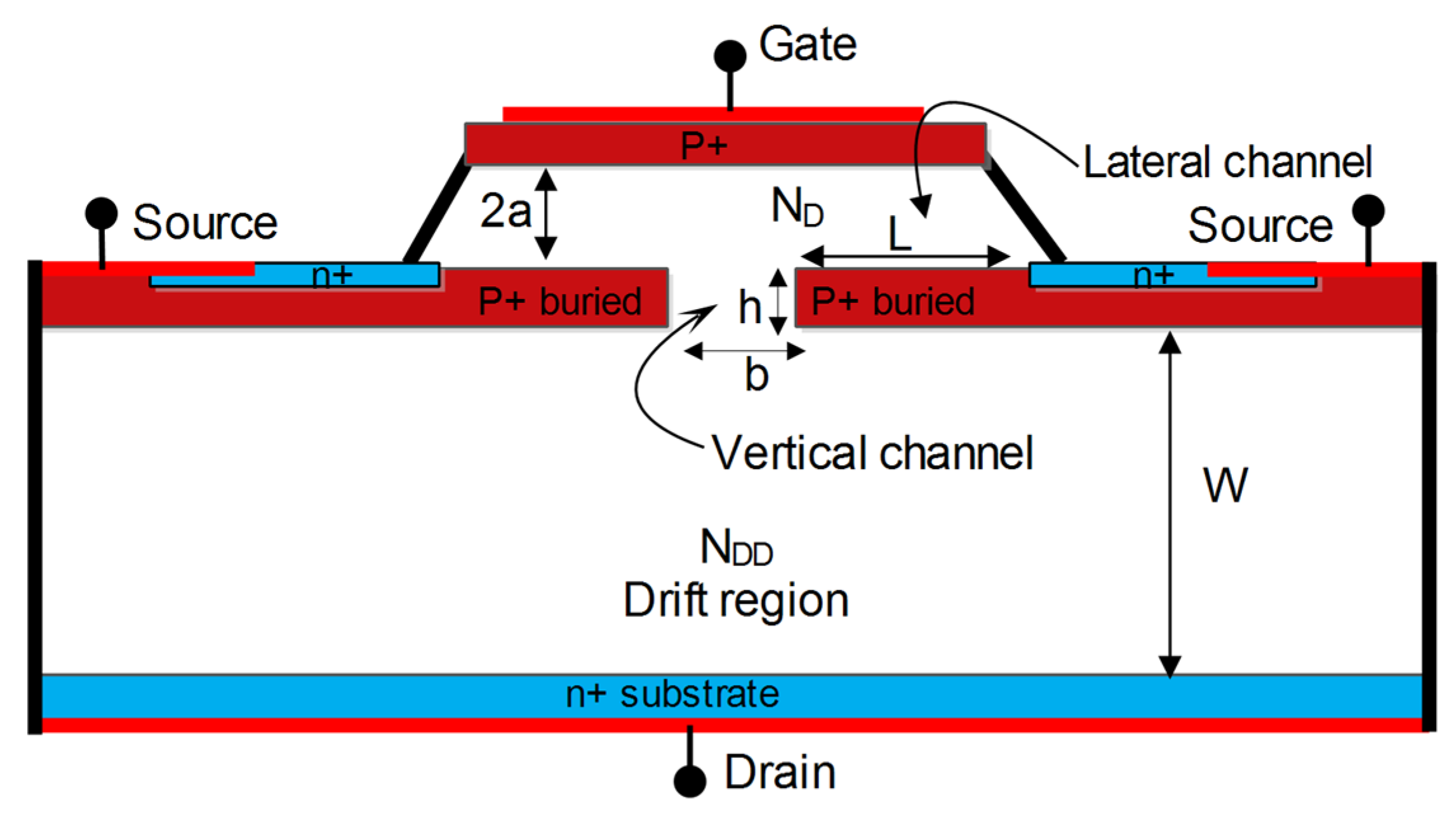
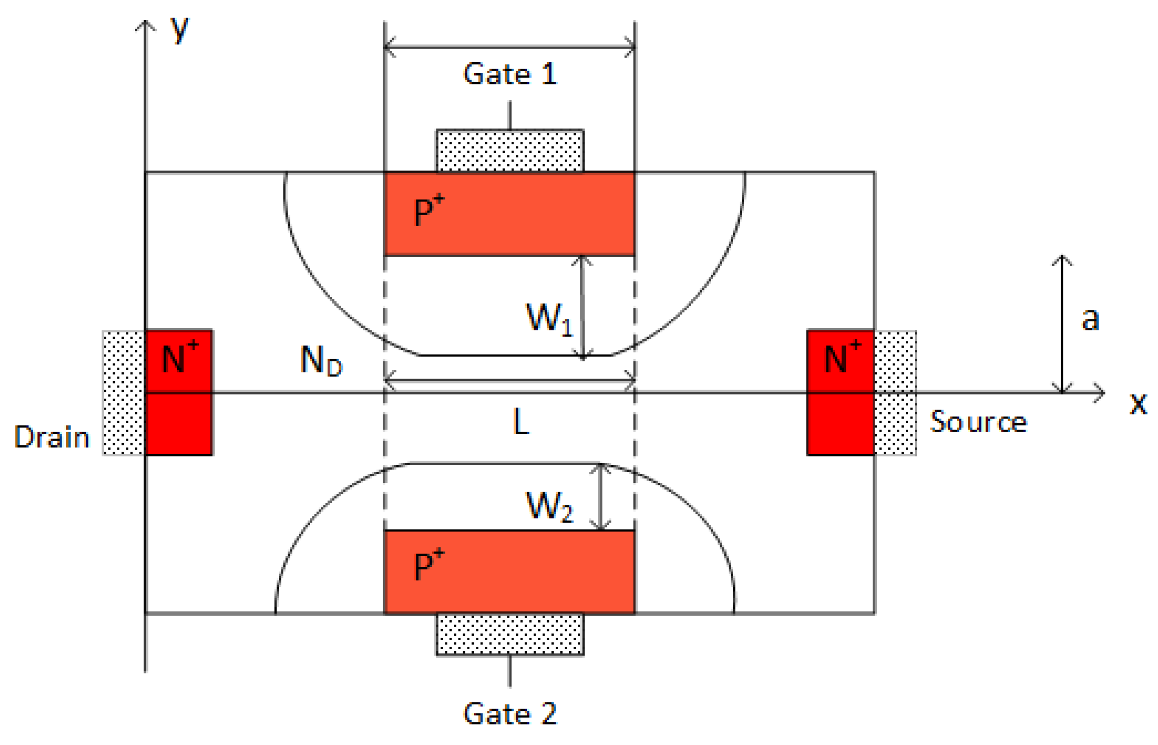
2. Analysis and Modeling of the Asymmetric Lateral Channel of the VJFET

This section concerns the analysis and the modeling of the behavior of the SiC LC-VJFET at blocking operation, which is controlled by the P+NP+ lateral channel. Figure 2 shows the lateral channel structure of Figure 1. This lateral channel controls asymmetrically the current in the device that is maintained by the difference in potentials between the two P+ layers, which are connected to the gate and source terminals, respectively. The asymmetry of the lateral channel does not concern the geometry, which is symmetric, but concerns the control of the channel. So, a model of the current distribution in the asymmetric lateral channel is needed.
In [26] the gradual channel approximation is used to derive the current flow in the asymmetrical lateral channel of the JFET. This approximation yields reasonably good results if the channel has a small width and large length and if the carrier mobility can be assumed to be constant and independent of the electric field [28].
Under this approximation, the channel current of the LC-VJFET can be derived analytically and may be expressed as:
I C H = q μ n N D Z ( 2 a W 1 ( x ) W 2 ( x ) ) d V d x
where a is the half of the channel width, Z is the equivalent width of the channel in the perpendicular direction, ND is the doping density of channel, W1 and W2 are the depletion layer widths under Gate 1 and Gate 2, respectively as clearly shown in Figure 2.
The drain current in the linear region is obtained by the integration of Equation (1) along the channel:
I C H = V P 3 R C H × { 3 V C H V P V P 3 / 2 × [ ( V b i + V C H V G 1 S ) 3 / 2 ( V b i V G 1 S ) 3 / 2 + ( V b i + V C H V G 2 S ) 3 / 2 ( V b i V G 2 S ) 3 / 2 ] }
where Vbi is the built-in voltage and is given by [29]:
V b i = k T q ln ( N A N D n i 2 ( T ) )
The intrinsic carrier concentration ni is expressed according to:
n i 2 ( T ) = N v N c e E G ( T ) k T
where Nv and Nc are the density of states in the valence and conduction bands, respectively, T the absolute temperature, k the constant of Boltzmann and EG(T) is the energy gap.
The pinch-off voltage VP and channel resistance RCH are defined as:
V P = q N D a 2 2 ε S i C
R C H = L 2 q μ n N D a Z
They have the same expression than in the symmetric channel model. So, for:
V G 1 S = V G 2 S = V G S
We can find the channel current in the symmetric case which is given by [28]:
I C H s y = V P 3 R C H × { 3 V C H V P 2 V P 3 / 2 × [ ( V b i + V C H V G S ) 3 / 2 ( V b i V G S ) 3 / 2 ] }
Since the channel voltage VCH is less than the saturation voltage VCHSAT the SiC JFET works in linear region. Beyond this value of saturation, the channel current will be saturated and the SiC JFET works in the saturation region. So, the saturation value is an important parameter, which represents the boundary between linear and saturation regions. This saturation region corresponds to the pinch-off operation which is reached when Equation (9) is valid:
W 1 ( x ) + W 2 ( x ) = 2 a
From Equation (9) the saturation voltage can be determined by taking into account the expressions of depletion layer widths W1 and W2 in the case of a uniformly doped channel with doping level ND:
W 1 ( x ) a =   1 V P ( V b i + V C H V G 1 S )
W 2 ( x ) a = 1 V P ( V b i + V C H V G 2 S )
Assuming that the pinch-off condition is reached for x = L. Using (10) and (11), Equation (9) allows to define the saturation voltage:
V C H S A T = V P V b i + V G 1 S + V G 2 S 2 + ( V G 1 S V G 2 S ) 2 16   V P
At this point the saturated drain current ICHSAT can be obtained from Equation (2) by using the standardized voltage values of the saturation voltage, the “Gate 1” to source voltage and the “Gate 2” to source voltage:
u C H S A T = V C H S A T V P
δ 1 = V b i V G 1 S V P
δ 2 = V b i V G 2 S V P
I C H S A T = V P 3 R C H × { 3 u C H S A T ( u C H S A T + δ 1 ) 3 / 2 ( u C H S A T + δ 2 ) 3 / 2 + δ 1 3 / 2 + δ 2 3 / 2 }
The saturated drain current can be calculated from this equation by substituting the drain voltage at pinch-off with Equation (12):
I C H S A T = V P 3 R C H Γ ( δ 1 ,   δ 2 )
with:
Γ ( δ 1 ,   δ 2 ) = 3 u C H S A T ( 1 + ( δ 2 δ 1 ) 2 16 δ 2 δ 1 2 ) 3 / 2 ( 1 + ( δ 2 δ 1 ) 2 16 + δ 2 δ 1 2 ) 3 / 2 + δ 1 3 / 2 + δ 2 3 / 2
In the symmetric case, δ 1 = δ 2 = δ and Equation (17) becomes:
I C H S A T S y ( δ ) = V P 3 R C H × { 1 3 δ + 2 δ 3 / 2 }
which is the classical saturation current for the symmetric JFET channel. In the blocking region:
V C H S A T s y = V P V b i + V G S 0
the channel current is zero, in particular for δ = 1 . Therefore, in the symmetric case, the classical condition of the blocking operation is expressed in the form of:
V G S V T h = V b i V P
where VTh is the classical threshold voltage. It is defined as the gate-to-source voltage value at which the saturation current becomes zero, ( I C H S A T S y ( V T h ) = 0 ).
However, it is much more complicated to find a simple threshold voltage model for asymmetric JFET channel. So, a numerical method can be adopted for solving the Equation (17). Figure 3 shows the plot of the Γ ( δ 1 ,   δ 2 ) function.
Figure 4, which is extracted from Figure 3 shows the curve Γ 0 which correspond to the pinch-off operation where the saturation current becomes null and satisfies this condition: Γ ( δ 1 ,   δ 2 ) reaches to:
Γ ( δ 1 0 ,   δ 2 0 ) = 0
where:
δ 1 0 = V b i V G S V P
In addition:
δ 2 0 = δ = V b i V P
Therefore, from the graphical representation of Figure 5 a relation between δ 1 0 and δ 2 0 can be implicitly given by:
δ 1 0 = Γ 0 ( δ )
which correspond to a blocking operation where the gate-to-source voltage reaches the threshold voltage value. At the blocking threshold V G S = V T h and Equation (23) may be rewritten as:
δ 1 0 = V b i V T h V P
which gives an implicitly expression of the threshold voltage:
V T h = V b i V P Γ 0 ( V b i V P )
This expression is based on a graphical representation which making it difficult to introduce in the circuit simulator, so an analytical threshold voltage model is needed.

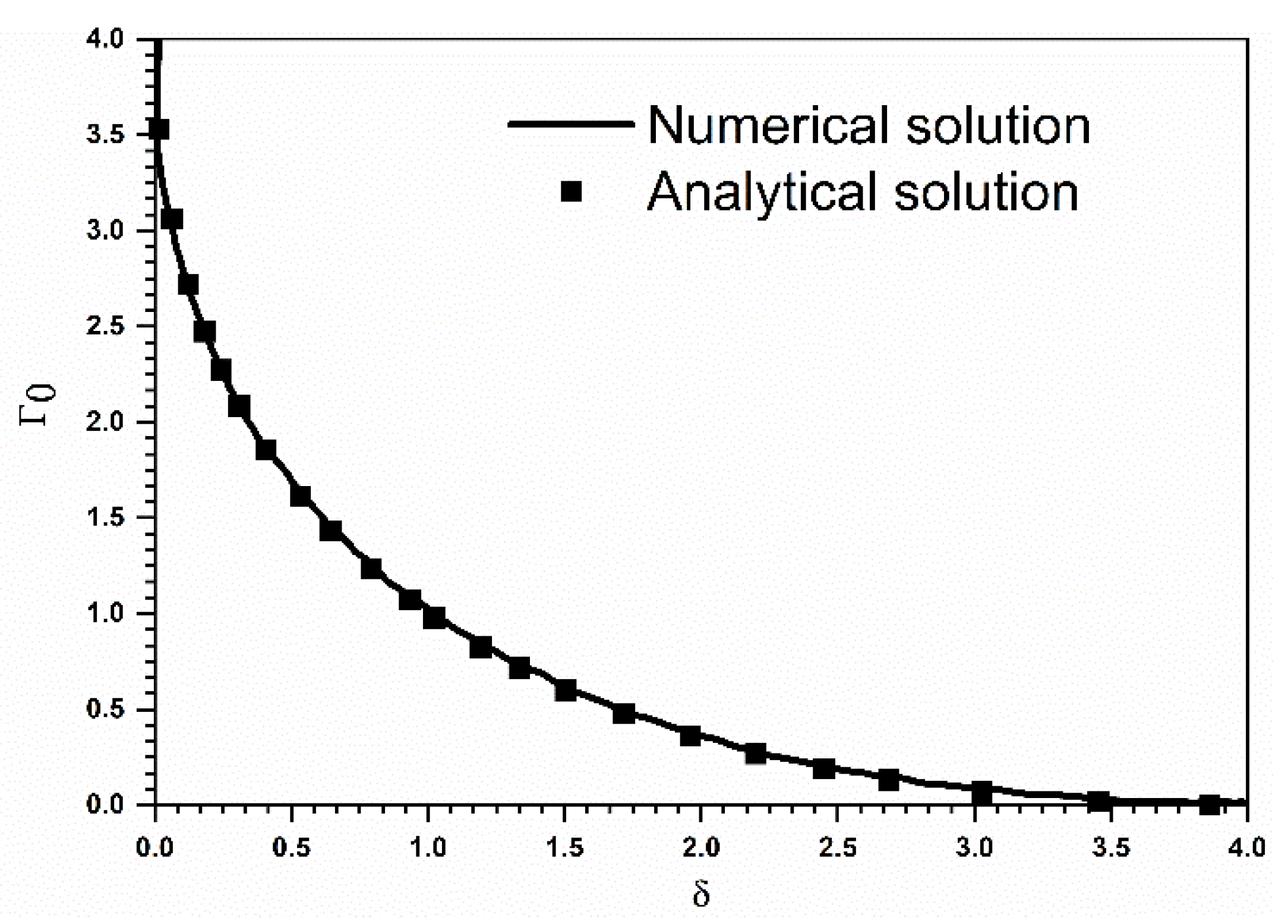
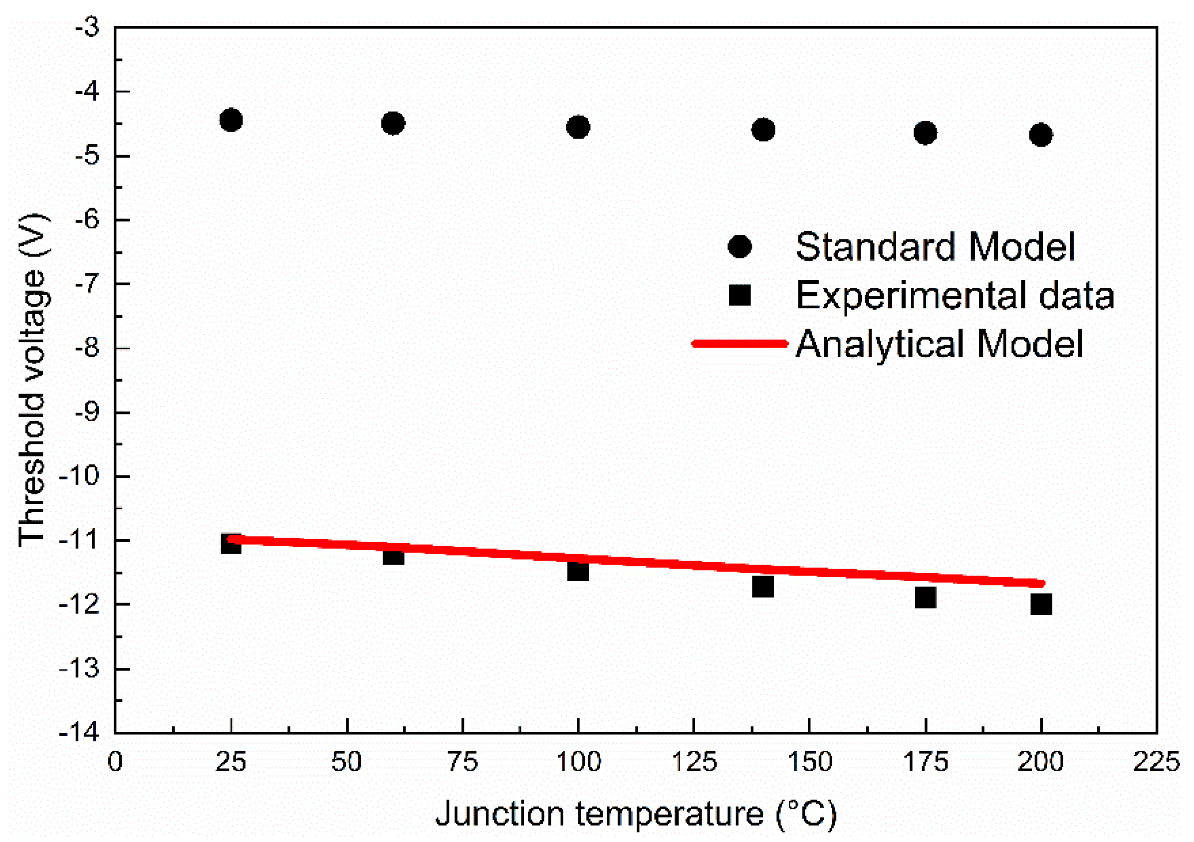
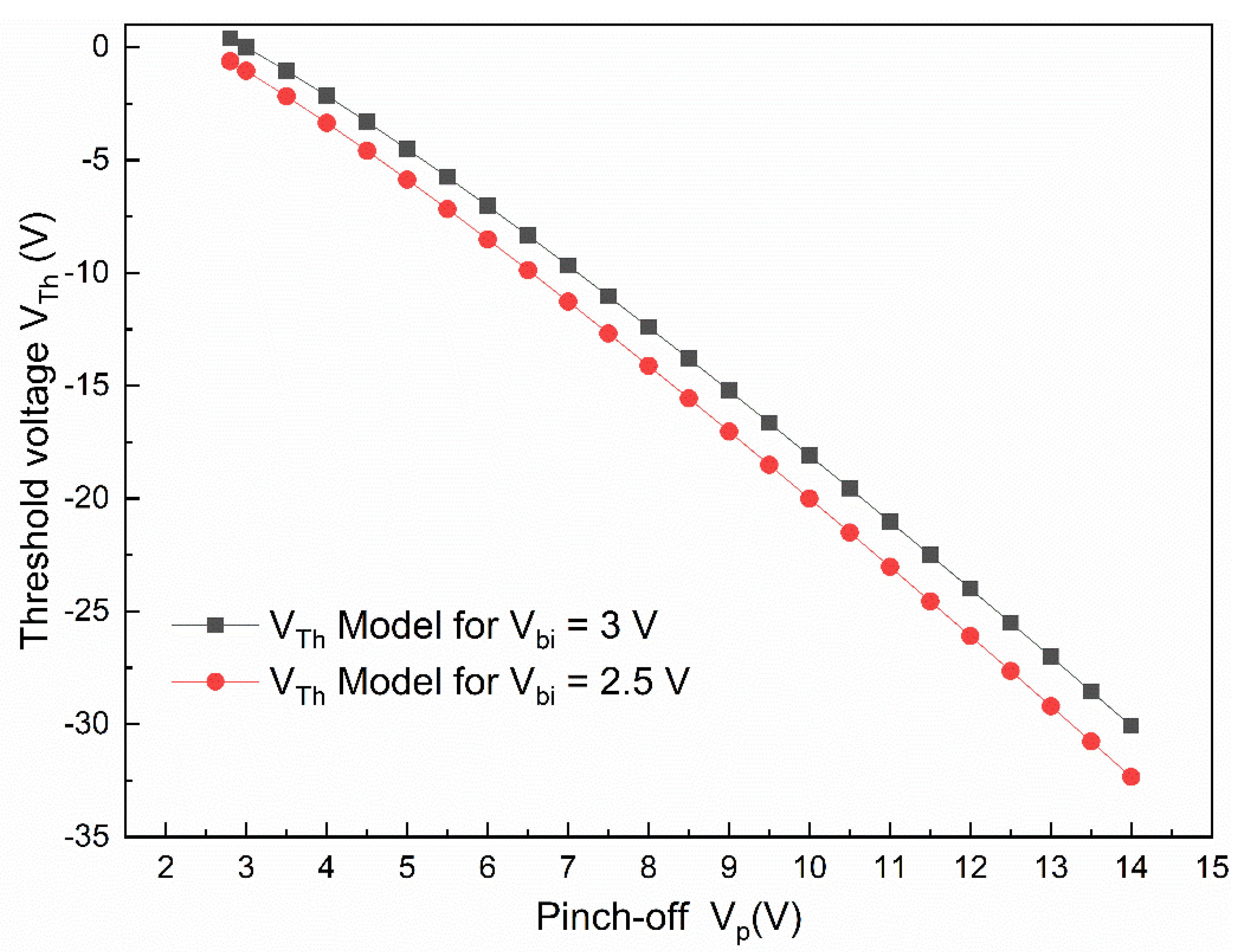
3. Threshold Voltage Model and Validation

In this section we proceed to develop the threshold voltage model based on the analysis of the potential distribution, φ, inside the lateral channel. To simplify the analysis, the gradual channel approximation is used to obtain a simple electric potential expression by solving the 1-D Poisson’s equation along the y-direction from the top gate “Gate 1” to the bottom gate “Gate 1”.
The 1-D Poisson equation can be written as [30]:
2 ϕ y 2 = q N D ε S i C
using the following boundary conditions:
ϕ ( 0 ) = V G 1 S
ϕ ( 2 a ) = 0
and assuming that at y = ym which is the maximum value of y when:
ϕ y = E = 0
In addition:
ϕ = ϕ m
in the case of a uniformly doped channel with doping level ND, an expression for the electrical potential is obtained:
ϕ ( y ) = ϕ m v P ( y y m a ) 2
using (29) and (30) conditions we would acquire:
V G 1 S = V G S = ϕ m v P ( y m a ) 2
In addition:
ϕ m = V p ( 2 y m a ) 2
substituting φm in (34) we obtain the expression for the depletion width value as function of the applied voltage VGS:
y m = a × ( 1 V G S 4 V P )
using (36), Equation (35) can be rewritten in the form of:
ϕ m = ϕ ( y m ) = V P × ( 1 + V G S 4 V P ) 2
By substituting Equations (36) and (37) in Equation (33), the expression for the electric potential is obtained as follows:
ϕ ( y ) = V G S V P × ( y 2 a 2 + 2 y a ( V G S 4 V P 1 ) )
which represents the variation of the electric potential as function of the applied voltage VGS.
The electrical potential evolution in the lateral channel under the blocking condition is analyzed by using a 2D TCAD physical simulator [31]. This analysis is based on many simulations by changing the parameters of the lateral channel (half width of the lateral channel “a” and the doping level “ND”). By considering the gradual channel approximation, the length L of the lateral channel was taken bigger than its width. The other typical parameters were taken from [25]. Referring to Figure 1, Table 1 summarizes the values of the doping concentrations and geometrical parameters used in this numerical simulation.
The numerical simulation results are presented in Figure 5 and Figure 6, which show that the electrical potential reaches its maximum φm at the point ym where the two space charge regions coincide. The first space charge region (SCR1) corresponds to the spreading of depletion layer under the top gate to achieve the width ym when the applied gate-source voltage becomes equal to the threshold gate voltage, which is given by:
y m = 2 a ω 0
where ω0 is the depletion-layer width of the second space charge region (SCR2) caused by the built-in potential (Vbi) when no voltage is applied to the bottom gate abrupt junction. Therefore, substituting (39) in (35), we obtain:
ϕ m = V p ( 2 2 a ω 0 a ) 2 = V p ( ω 0 a ) 2 = q N D 2 ε S i C ω 0 2
which corresponds well to the built-in potential (Vbi) producing the depletion layer given by [30]:
ω 0 = 2 ε S i C q N D V b i
A vertical cut from “Gate 1” to “Gate 2” has been accomplished on Figure 5 and from this cut we obtained the electric potential distribution along the channel of the SiC LC-VJFET structure and is illustrated in Figure 6.
Furthermore, as illustrated in Figure 6 when Vgs reaches VTh, the electrical potential φm reaches Vbi and Equation (37) can be rewritten in the form of:
V b i = V P × ( 1 + V T h 4 V P ) 2
which yields to the following expression:
V T h = V b i V P ( 2 V b i V P ) 2
Equation (43) represents the new model of threshold voltage which corresponds to the same expression (27) cited above when:
Γ 0 ( δ ) = ( 2 δ ) 2
This result is validated and shown in Figure 7. We obtained a good agreement between analytical expression given in Equation (44) and the numerical solution of Γ 0 function given in Figure 4.
So, we have developed a novel approach of the asymmetrical threshold voltage channel different from the standard JFET model given by the classical expression:
V T h = V b i V P
Figure 8 demonstrates the calculated values of the threshold voltage model compared with the experimental results for a wide temperature range. The experimental data as well as the pinch-off voltage and the lateral channel doping concentration used in the calculation of the threshold voltage model are reported in [27] and are given by:
Vp = 7.29 V and ND = 1.64 × 1016 cm−3
It is seen from the figure an excellent agreement between the model and experimental results is observed. This confirms the validity of the suggested threshold voltage model. It is also clear that there is a big difference between the standard model of threshold voltage (given by Equation (45)) and the analytical model results, thus cannot describe well enough the behavior of threshold voltage of the studied device.
Figure 9 depicts the dependence of threshold voltage versus the Pinch-off voltage using the proposed model for two different built-in voltages.
Since it is too difficult to determine the Vp value directly from the analytical model which is presented as an implicit expression, Figure 9 serves as a chart tool for parameter extraction. Knowing its threshold voltage experimentally, one can easily extract the pinch-off voltage value and then estimate geometric and doping parameters of the device.

4. Conclusions

This paper focuses essentially on the physical analysis of the behavior of the SiC LC-VJFET with lateral channel in the blocking mode. The difficulty posed by this device is that the blockage is controlled asymmetrically by the lateral channel. The asymmetry concerns the difference of the applied gate voltages between the two P+ layers and not the geometry of the channel structure which is symmetric. The blocking condition of the power device has not been previously solved correctly. To address this problem, this work was investigated to accurately propose an analytical model of the gate to source threshold voltage which is a main parameter that controls the blockage of the device.
So, a temperature dependent analytical model for the threshold voltage of the power device SiC LC-VJFET has been derived under two steps: Firstly, numerical method has been adopted to solve the saturation current which allows to a graphical solution of the blocking condition. Secondly, a physical analysis of the electric potential distribution in the asymmetric side-channel blocking condition leads to an analytical solution which was validated regarding the graphical solution and numerical simulation. The model is compared with experimental data for a wide temperature range. Good agreement has been observed demonstrating the accuracy of the proposed model.

Author Contributions

Modelling and simulation, S.G. and A.F.; writing—original draft preparation, S.G.; writing—review and analysis, S.G. and A.F.; review and editing, S.G. and K.B. All authors have read and agreed to the published version of the manuscript.

Funding

This research received no external funding.

Conflicts of Interest

The authors declare no conflict of interest.

References

  1. Ortiz-Conde, A.; García Sánchez, F.J.; Liou, J.J.; Cerdeira, A.; Estrada, M.; Yue, Y. A review of recent MOSFET threshold voltage extraction methods. Microelectron. Reliab. 2002, 42, 583–596. [Google Scholar] [CrossRef]
  2. Tsormpatzoglou, A.; Tassis, D.H.; Dimitriadis, C.A.; Ghibaudo, G.; Collaert, N.; Pananakakis, G. Analytical threshold voltage model for lightly doped short-channel tri-gate MOSFETs. Solid-State Electron. 2011, 57, 31–34. [Google Scholar] [CrossRef]
  3. Tsormpatzoglou, A.; Pappas, I.; Tassis, D.H.; Dimitriadis, C.A.; Ghibaudo, G. Analytical threshold voltage model for short-channel asymmetrical dual-gate material double-gate MOSFETs. Microelectron. Eng. 2012, 90, 9–11. [Google Scholar] [CrossRef]
  4. Ortiz-Conde, A.; García-Sánchez, F.J.; Muci, J.; Terán Barrios, A.; Liou, J.J.; Ho, C.-S. Revisiting MOSFET threshold voltage extraction methods. Microelectron. Reliab. 2013, 53, 90–104. [Google Scholar] [CrossRef]
  5. Aichinger, T.; Rescher, G.; Pobegen, G. Threshold voltage peculiarities and bias temperature instabilities of SiC MOSFETs. Microelectron. Reliab. 2018, 80, 68–78. [Google Scholar] [CrossRef]
  6. Guevara, E.; Herrera-Pérez, V.; Rocha, C.; Guerrero, K. Threshold Voltage Degradation for n-Channel 4H-SiC Power MOSFETs. J. Low Power Electron. Appl. 2020, 10, 3. [Google Scholar] [CrossRef] [Green Version]
  7. Friedrichs, P.; Stephani, D. Unipolar SiC power devices and elevated temperature. Microelectron. Eng. 2006, 83, 181–184. [Google Scholar] [CrossRef]
  8. Gachovska, T.K.; Hudgins, J.L. 5-SiC and GaN Power Semiconductor Devices. In Power Electronics Handbook, 4th ed.; Rashid, M.H., Ed.; Butterworth-Heinemann: Oxford, UK, 2018; pp. 95–155. [Google Scholar]
  9. Ji, D.; Chowdhury, S. Design of 1.2 kV Power Switches with Low RON Using GaN-Based Vertical JFET. IEEE Trans. Electron. Devices 2015, 62, 2571–2578. [Google Scholar] [CrossRef]
  10. Kaneko, M.; Kimoto, T. High-Temperature Operation of n- and p-Channel JFETs Fabricated by Ion Implantation into a High-Purity Semi-Insulating SiC Substrate. IEEE Electron. Device Lett. 2018, 39, 723–726. [Google Scholar] [CrossRef]
  11. Huang, H.; Li, F.; Sun, Z.; Sun, N.; Zhang, F.; Cao, Y.; Zhang, H.; Tao, P. Gallium Nitride Normally-Off Vertical Field-Effect Transistor Featuring an Additional Back Current Blocking Layer Structure. Electronics 2019, 8, 241. [Google Scholar] [CrossRef] [Green Version]
  12. Barbagallo, C.; Rizzo, S.A.; Scelba, G.; Scarcella, G.; Cacciato, M. On the Lifetime Estimation of SiC Power MOSFETs for Motor Drive Applications. Electronics 2021, 10, 324. [Google Scholar] [CrossRef]
  13. Kizilyalli, I.C.; Aktas, O. Characterization of vertical GaN p–n diodes and junction field-effect transistors on bulk GaN down to cryogenic temperatures. Semicond. Sci. Technol. 2015, 30, 124001. [Google Scholar] [CrossRef] [Green Version]
  14. Li, H.; Liao, X.; Hu, Y.; Huang, Z.; Wang, K. Analysis of Voltage Variation in Silicon Carbide MOSFETs during Turn-On and Turn-Off. Energies 2017, 10, 1456. [Google Scholar] [CrossRef] [Green Version]
  15. Alonso, A.R.; Díaz, M.F.; Lamar, D.G.; Azpeitia, M.A.P.d.; Hernando, M.M.; Sebastián, J. Switching Performance Comparison of the SiC JFET and SiC JFET/Si MOSFET Cascode Configuration. IEEE Trans. Power Electron. 2014, 29, 2428–2440. [Google Scholar] [CrossRef] [Green Version]
  16. Elpelt, R.; Friedrichs, P.; Biela, J. Fast Switching with SiC VJFETs-Influence of the Device Topology. Mater. Sci. Forum 2010, 645–648, 933–936. [Google Scholar] [CrossRef]
  17. Veliadis, V. Silicon Carbide Junction Field-Effect Transistors (SiC JFETs). In Wiley Encyclopedia of Electrical and Electronics Engineering; John Wiley & Sons: Linthicum, MD, USA, 2014; pp. 1–37. [Google Scholar]
  18. Neudeck, P.G.; Spry, D.J.; Chen, L.Y. Experimental and Theoretical Study of 4H-SiC JFET Threshold Voltage Body Bias Effect from 25 °C to 500 °C. Mater. Sci. Forum 2016, 858, 903–907. [Google Scholar] [CrossRef]
  19. Kayambaki, M.; Makris, N.; Stavrinidis, A.; Konstantinidis, G.; Zekentes, K. On the Optimum Determination and Use of SiC VJFET Threshold Voltage. Mater. Sci. Forum 2018, 924, 657–660. [Google Scholar] [CrossRef]
  20. Asllani, B.; Bevilacqua, P.; Zaoui, A.; Grosset, G.; Planson, D.; Morel, H. High-Voltage SiC-JFET Fabrication and Full Characterization. Mater. Sci. Forum 2019, 963, 688–692. [Google Scholar] [CrossRef] [Green Version]
  21. Fernández-Martínez, P.; Flores, D.; Hidalgo, S.; Jordà, X.; Perpiñà, X.; Quirion, D.; Ré, L.; Ullán, M.; Vellvehí, M. A New Vertical JFET Power Device for Harsh Radiation Environments. Energies 2017, 10, 256. [Google Scholar] [CrossRef] [Green Version]
  22. Bargieł, K.; Bisewski, D.; Zarębski, J. Modelling of Dynamic Properties of Silicon Carbide Junction Field-Effect Transistors (JFETs). Energies 2020, 13, 187. [Google Scholar] [CrossRef] [Green Version]
  23. Zhang, Y.; Tang, M.; Song, Q.; Tang, X.; Lv, H.; Liu, S. High temperature characterization of normally-on 4H-SiC junction field-effect transistor. Superlattices Microstruct. 2016, 99, 113–117. [Google Scholar] [CrossRef]
  24. Grekov, A.E.; Chen, Z.; Fu, R.; Hudgins, J.L.; Mantooth, H.A.; Sheridan, D.C.; Casady, J.; Santi, E. Parameter Extraction Procedure for Vertical SiC Power JFET. IEEE Trans. Ind. Appl. 2011, 47, 1862–1871. [Google Scholar] [CrossRef]
  25. Ghedira, S.; Buttay, C.; Morel, H.; Besbes, K. Measurement and numerical analysis of C-V characteristics for normally-on SiCED-JFET. Eur. Phys. J. Appl. Phys. 2014, 66, 20103. [Google Scholar] [CrossRef]
  26. Hervé, M.; Youness, H.; Dominique, T.; Rémi, R.; Fabien, D.; Damien, R.; Christian, M.; Dominique, B.; Cyril, B.; Régis, M. A multi-physics model of the VJFET with a lateral channel. In Proceedings of the 2011 14th European Conference on Power Electronics and Applications, Birmingham, UK, 30 August–1 September 2011; pp. 1–10. [Google Scholar]
  27. Dubois, F.; Bergogne, D.; Tournier, D.; Buttay, C.; Meuret, R.; Morel, H. Analysis of the SiC VJFET gate punch-through and its dependence with the temperature. In Proceedings of the 2013 15th European Conference on Power Electronics and Applications (EPE), Lille, France, 2–6 September 2013; pp. 1–10. [Google Scholar]
  28. Baliga, B.J. Modern Power Devices; Wiley: Hoboken, NJ, USA, 1987. [Google Scholar]
  29. Baliga, B.J. Fundamentals of Power Semiconductor Devices; Springer International Publishing: Berlin/Heidelberg, Germany, 2018. [Google Scholar]
  30. Sze, S.M.; Lee, M.K. Semiconductor Devices: Physics and Technology; John Wiley & Sons: New York, NY, USA, 2013. [Google Scholar]
  31. Synopsys. Sentaurus Device User Guide, Version F-2011.09 ed.; Synopsys: Mountain View, CA, USA, 2011. [Google Scholar]
Figure 1. Structure of the SiC LC-VJFET investigated device.
Electronics 10 01494 g001
Figure 2. Channel structure of the SiC LC-VJFET investigated device.
Electronics 10 01494 g002
Figure 3. Function that presents regular and positive function.
Electronics 10 01494 g003
Figure 4. Numerical Solution of Γ0 function extracted from Figure 3.
Electronics 10 01494 g004
Figure 5. 2D numerical simulation of the device showing the overlap of the space charge regions 1 and 2.
Electronics 10 01494 g005
Figure 6. Numerical simulation of the electric Potential distribution along the lateral channel of the SiC LC-VJFET structure.
Electronics 10 01494 g006
Figure 7. Comparison of Analytical and Numerical solutions of Γ0(δ) function.
Electronics 10 01494 g007
Figure 8. Comparison of the threshold voltage model with Experimental values over a wide range of Temperature.
Electronics 10 01494 g008
Figure 9. Graphical representation of threshold voltage model versus the Pinch-off voltage for two different values of Vbi.
Electronics 10 01494 g009
Table 1. Geometrical and Doping parameters values used in the simulations.
SymbolDefinitionValue
aHalf width of the lateral channel0.72 µm
LLength of the lateral channel6 µm
NDDoping level in the lateral channel2.4 × 1016 cm−3
NADopping in the gate1 × 1018 cm−3
WThickness of the epilayer15 µm
NDDDoping level in the epilayer5 × 1015 cm−3
hWidth of the vertical channel0.7 µm
bLength of the vertical channel2.6 µm
Publisher’s Note: MDPI stays neutral with regard to jurisdictional claims in published maps and institutional affiliations.

