
A 77-GHz High Gain Low Noise Receiver for Automatic Radar Applications


Abstract
:1. Introduction
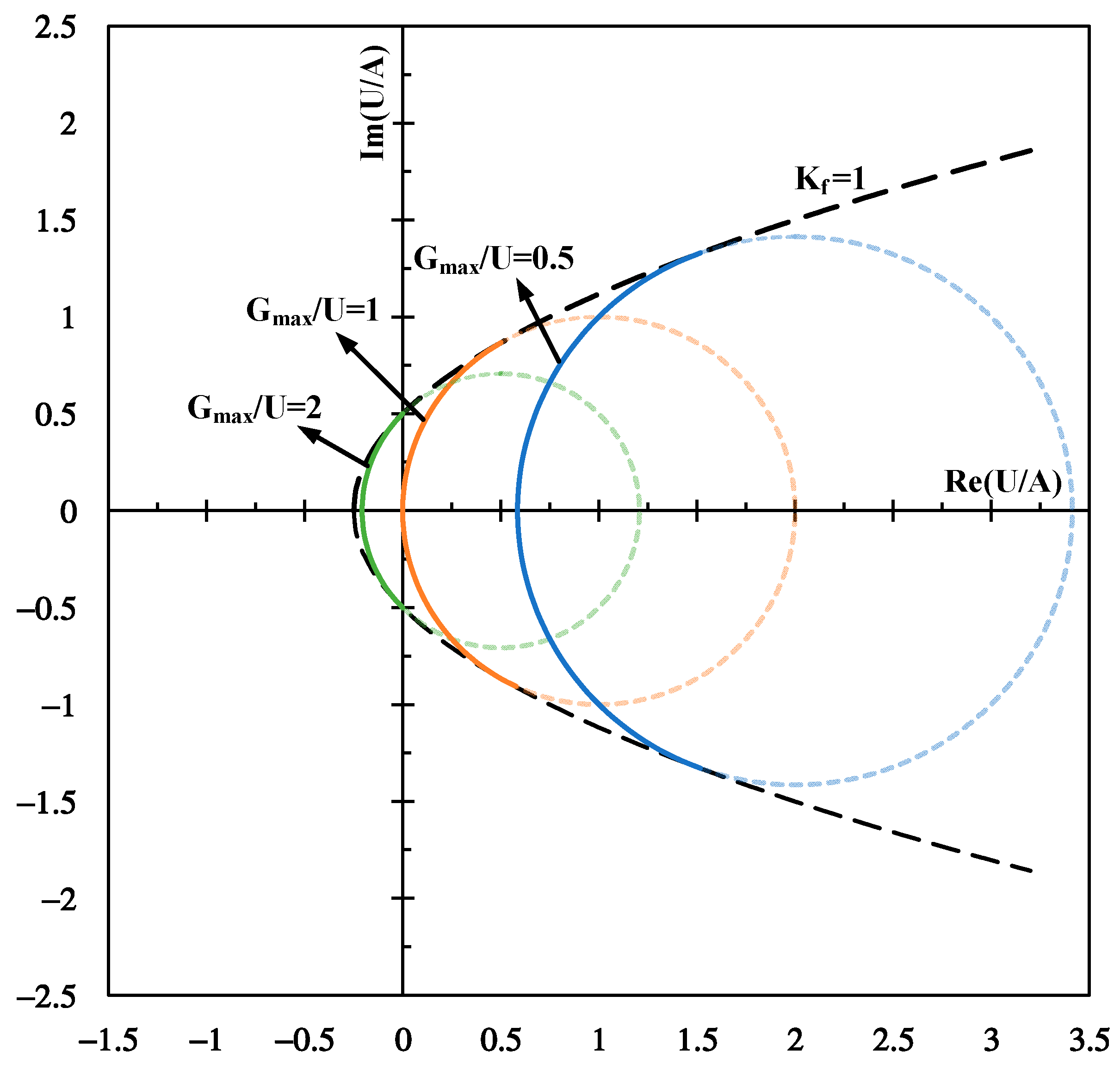
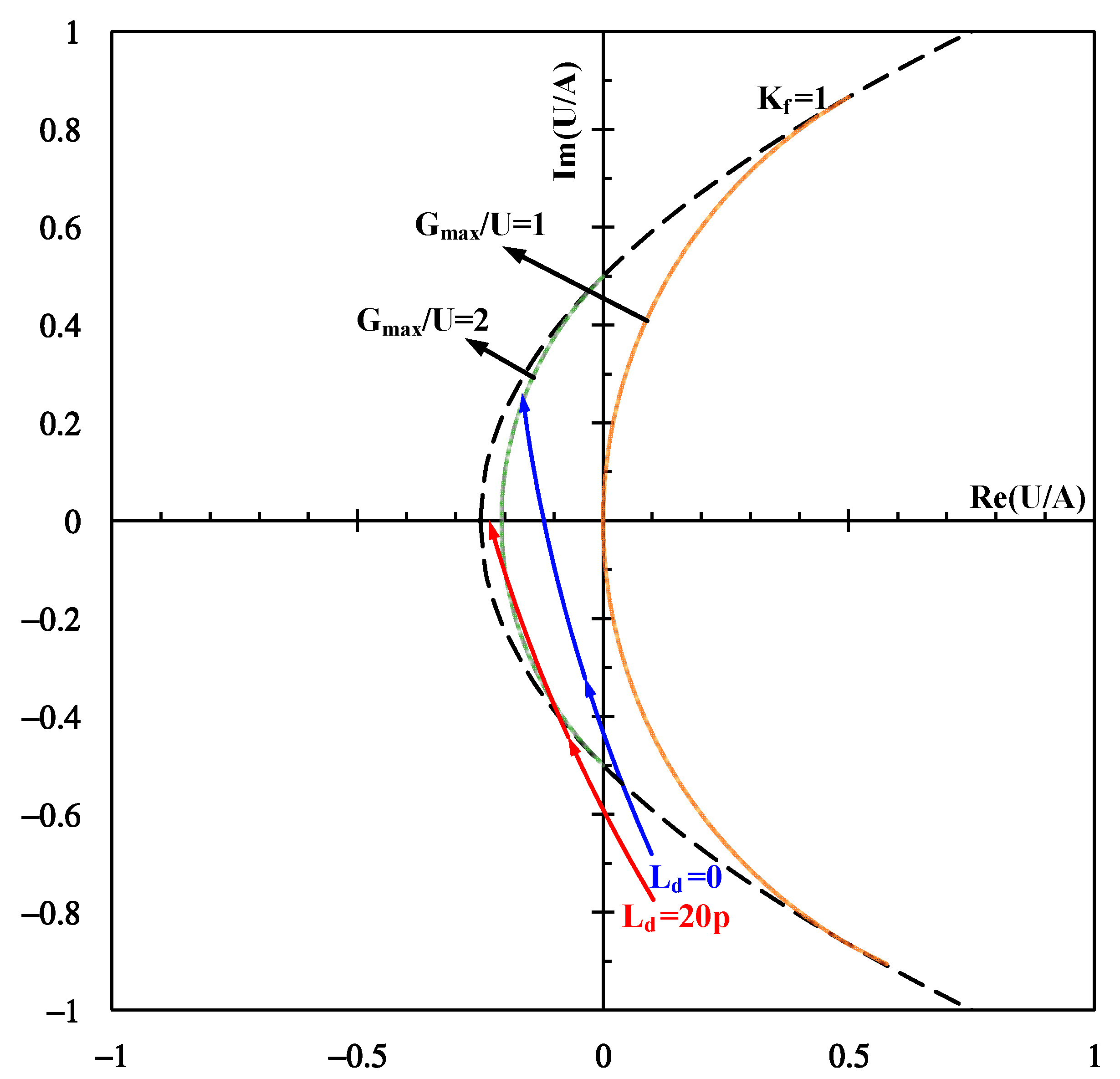
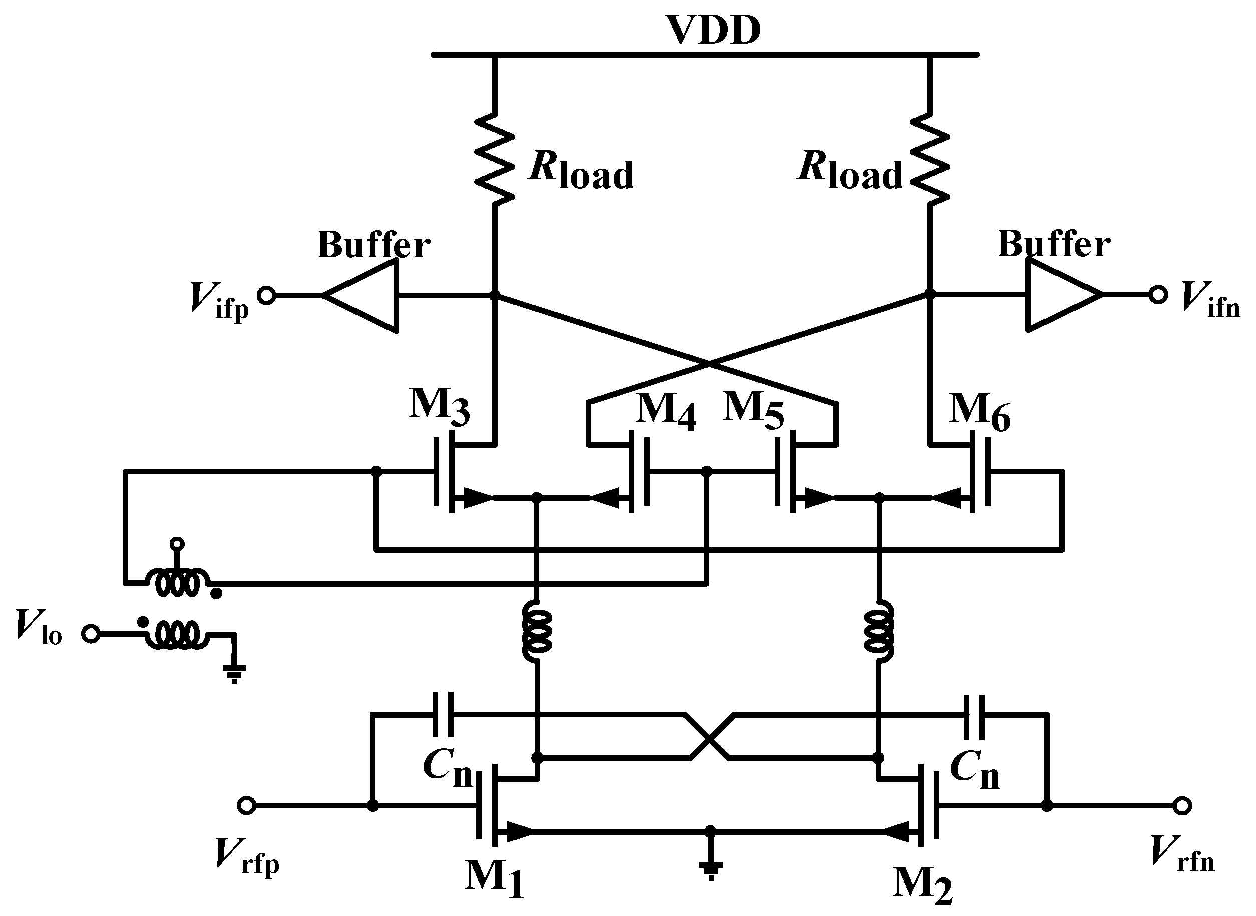
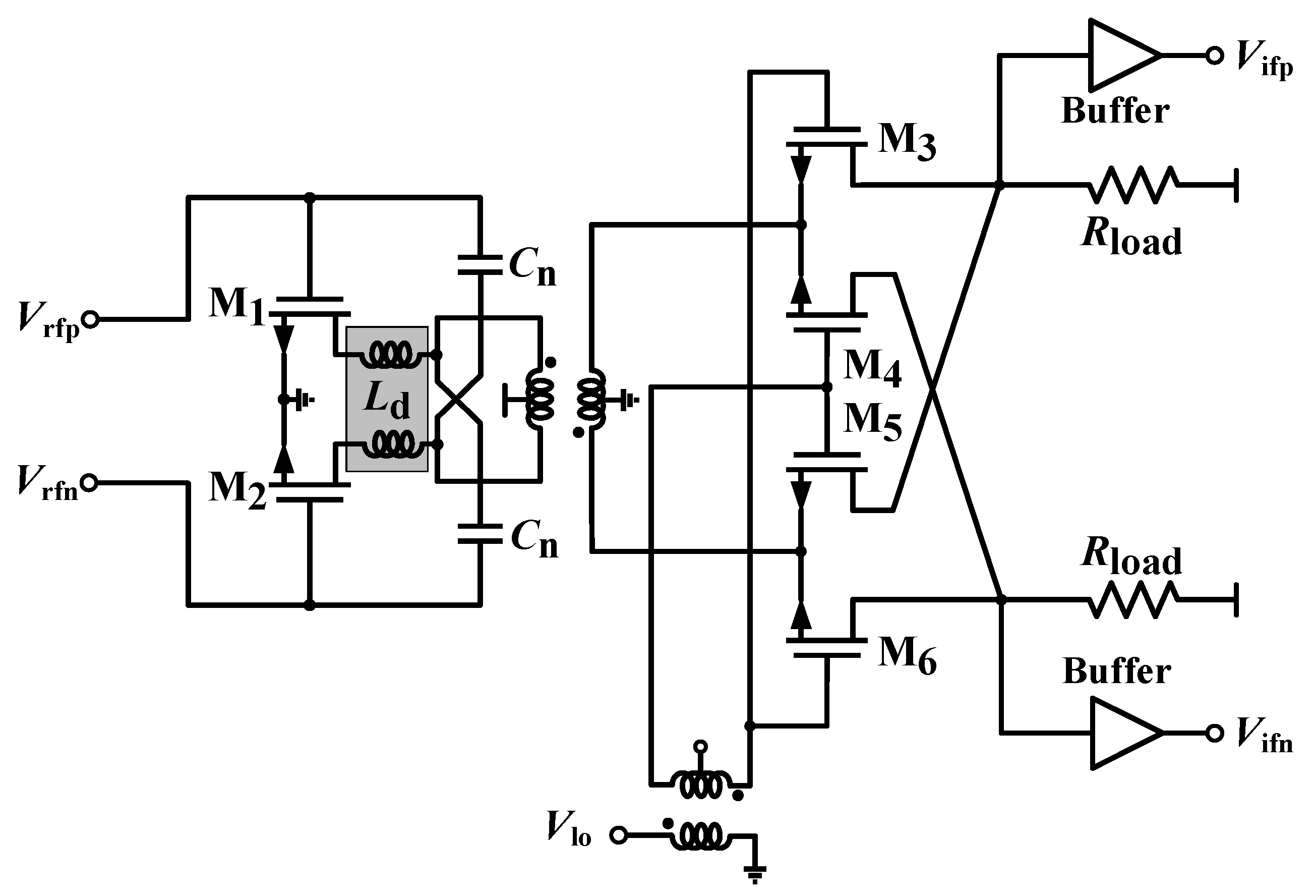
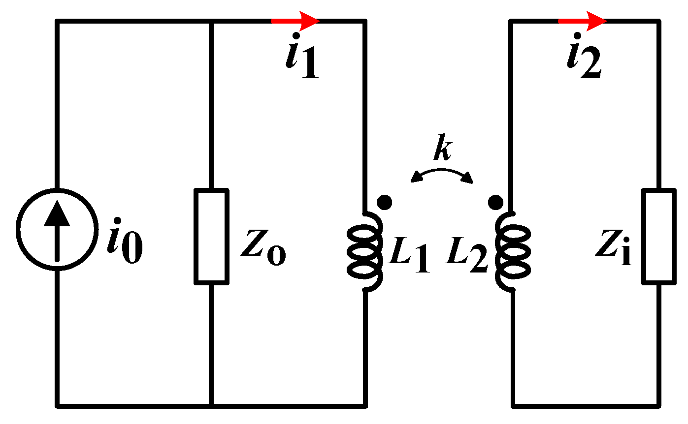
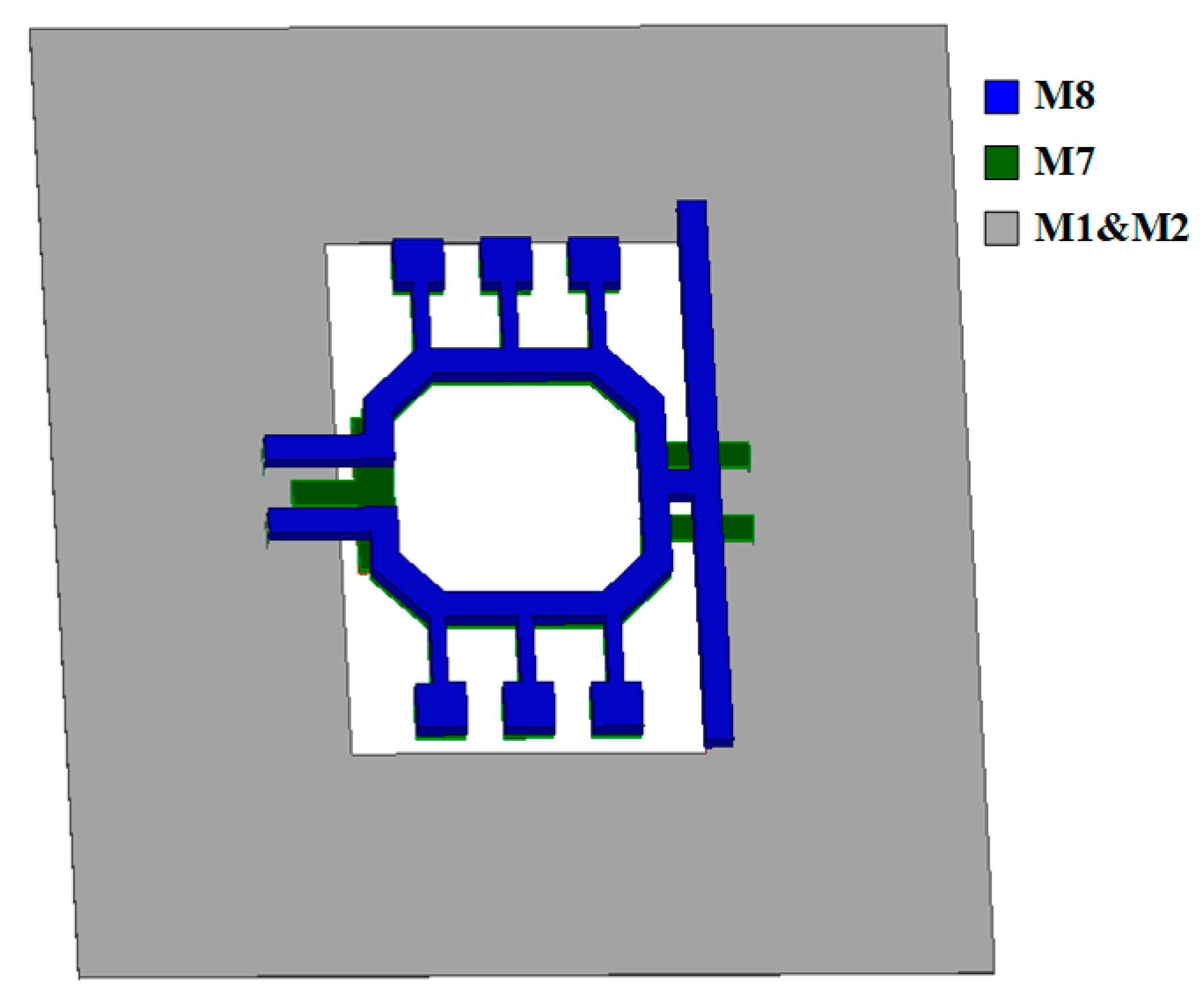
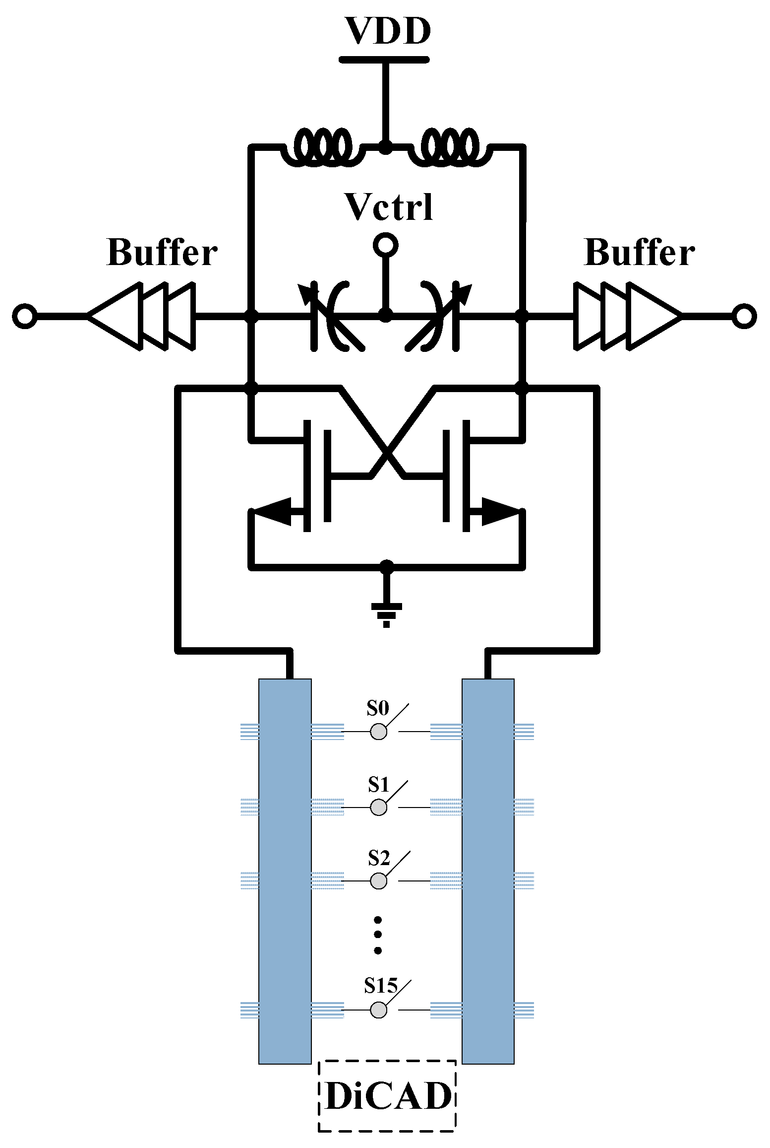
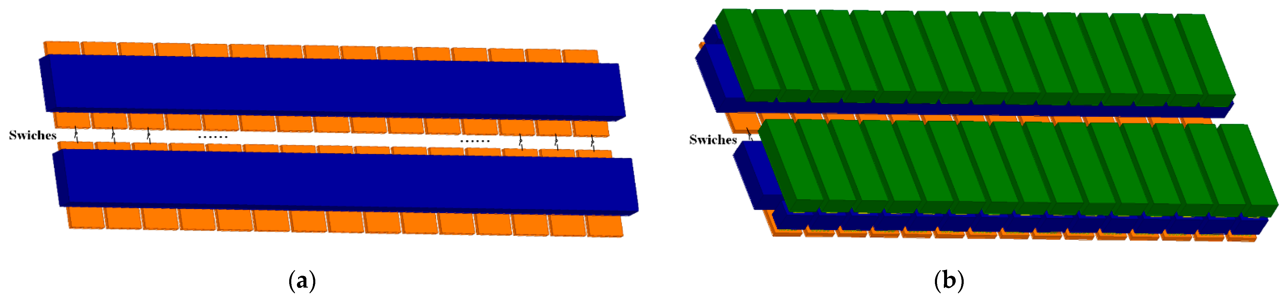
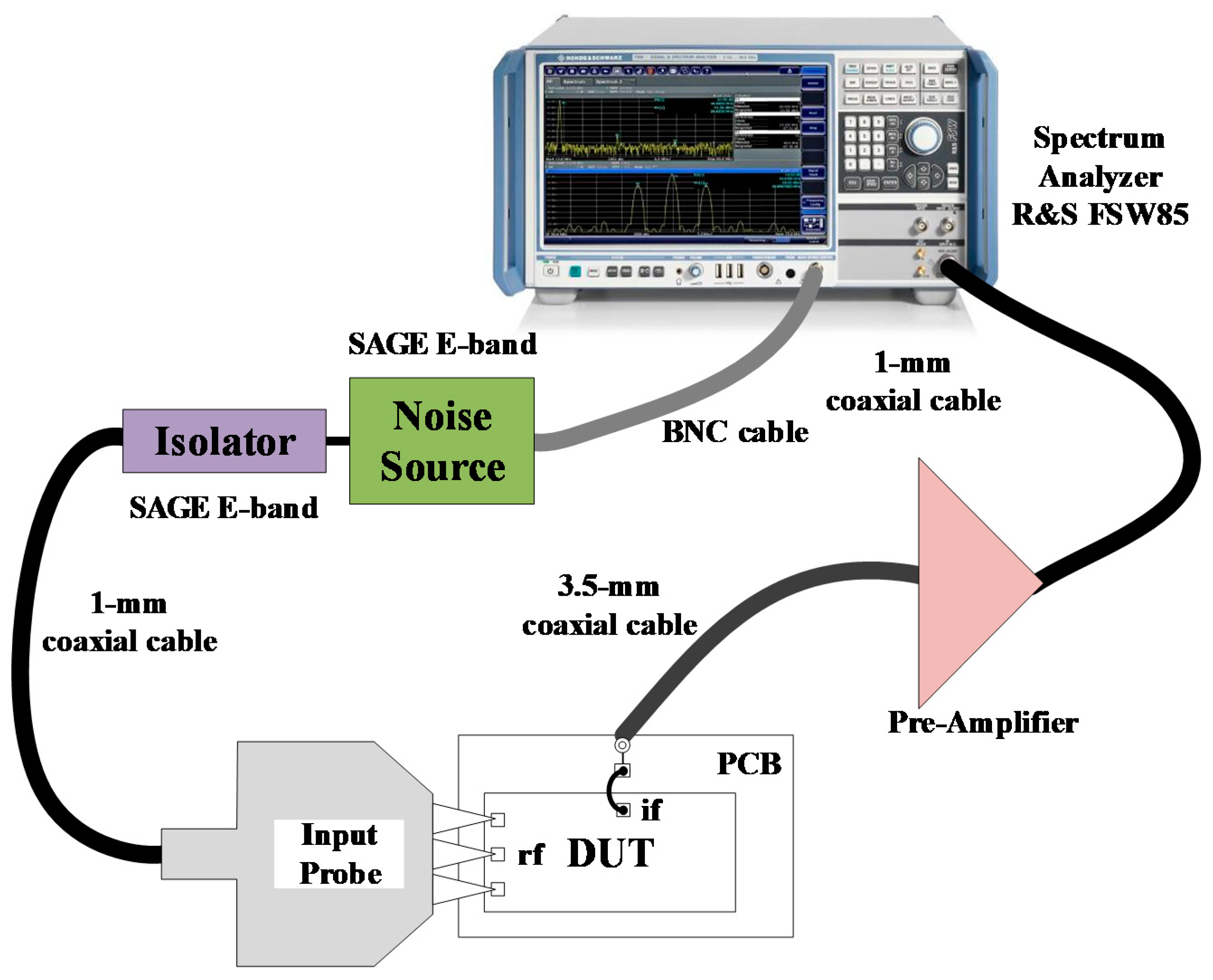
2. Receiver Design
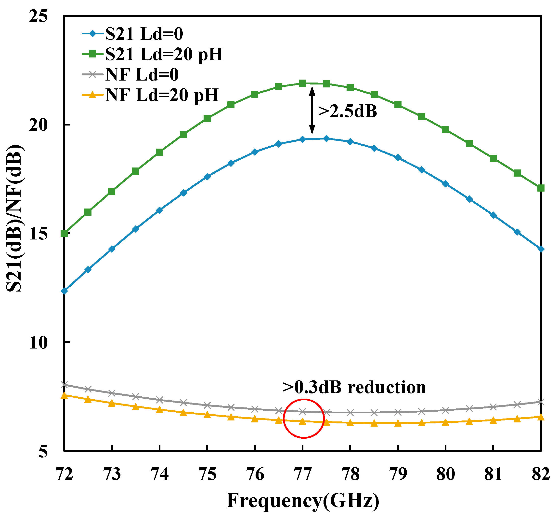
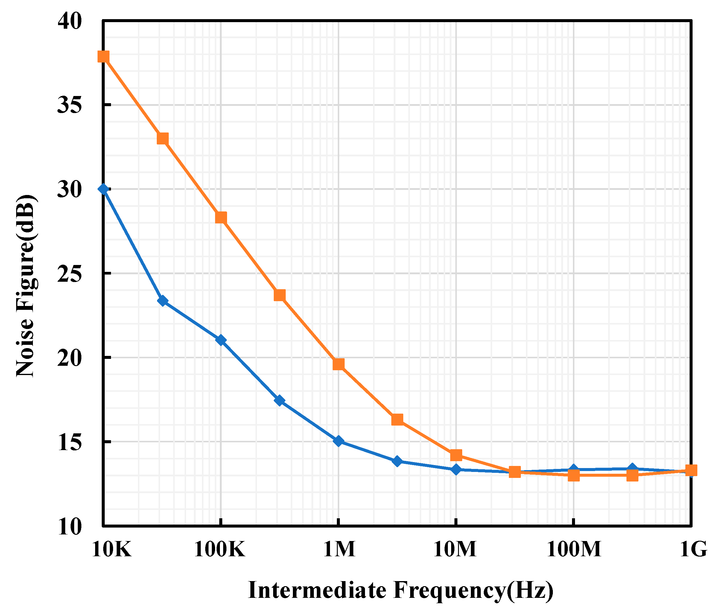
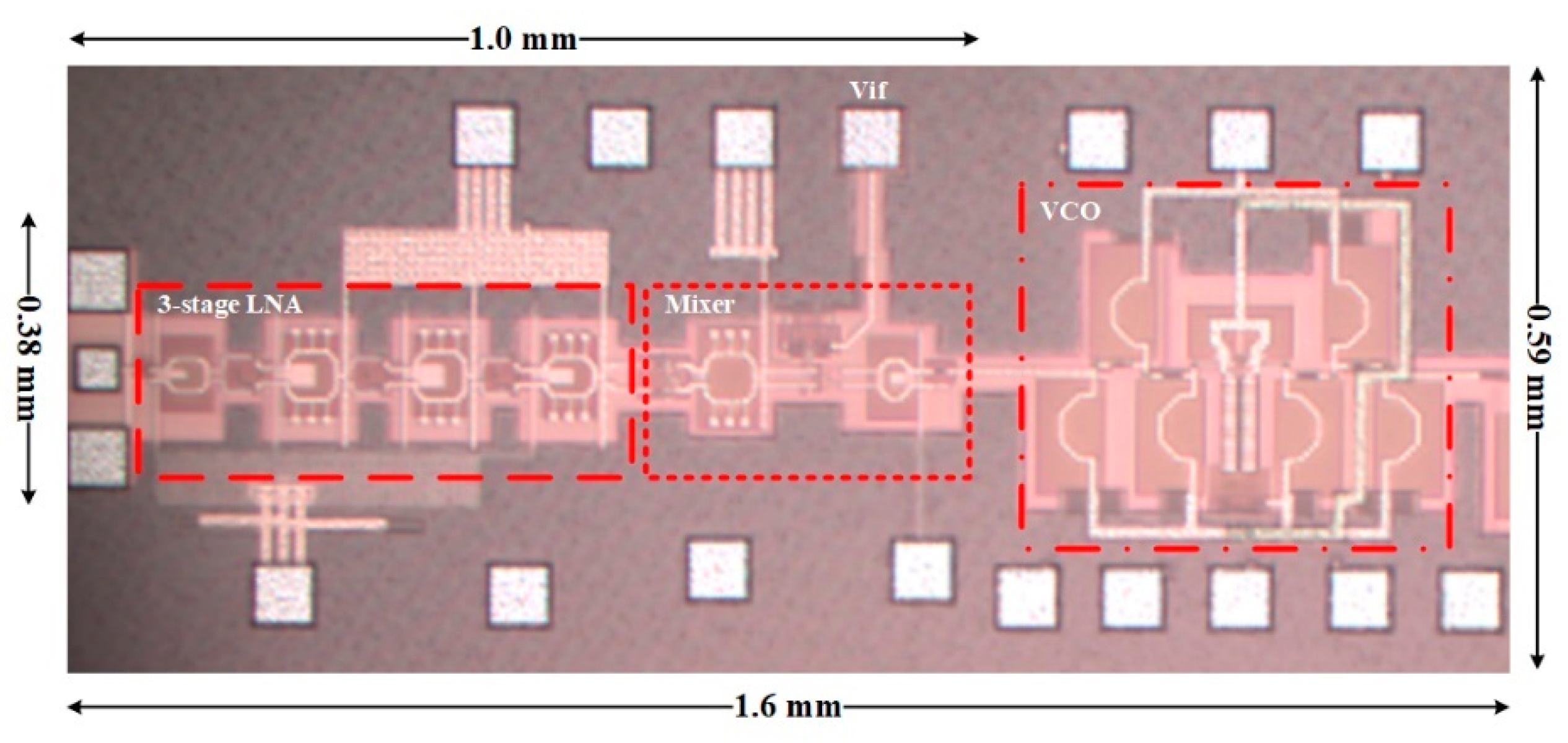
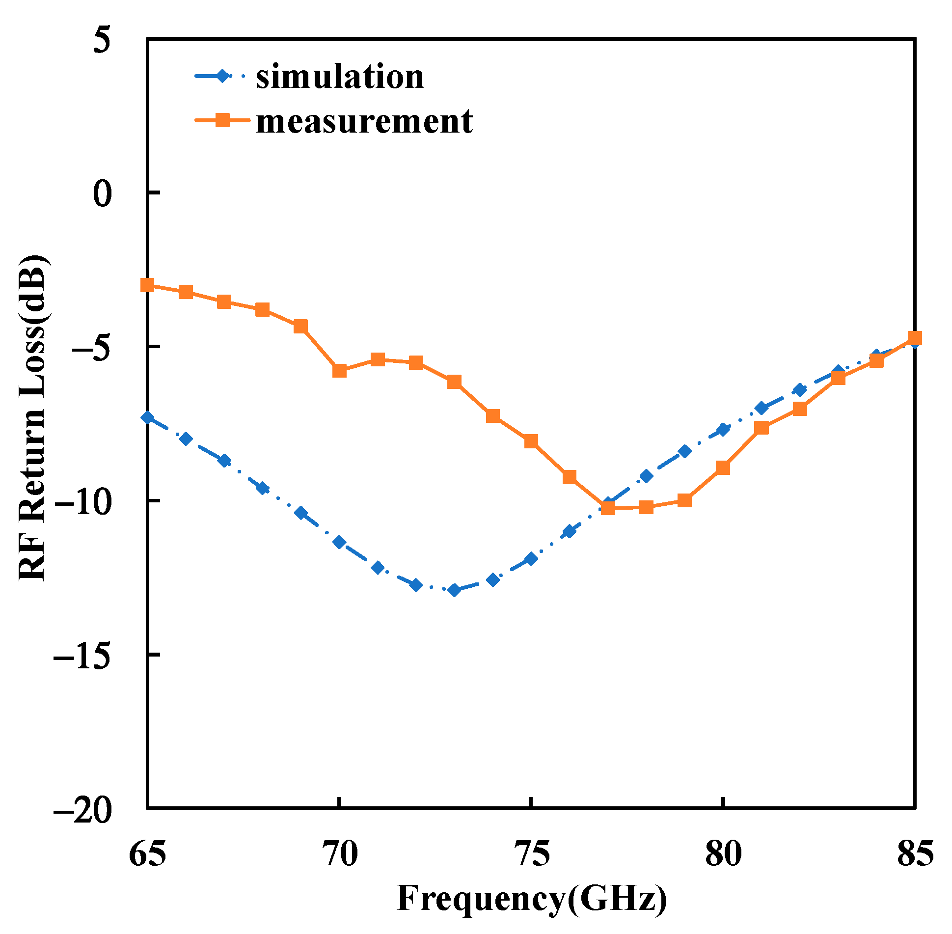
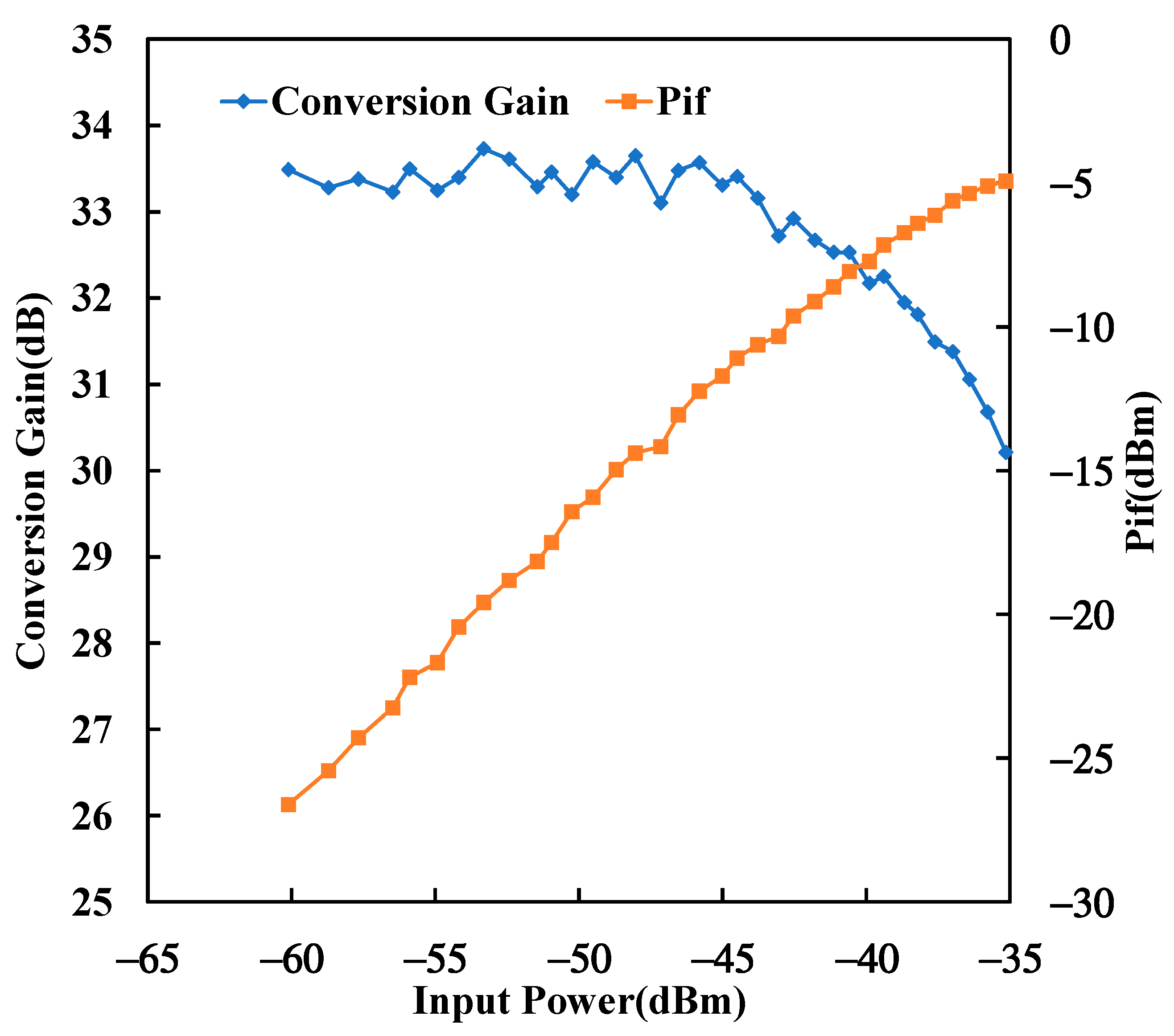
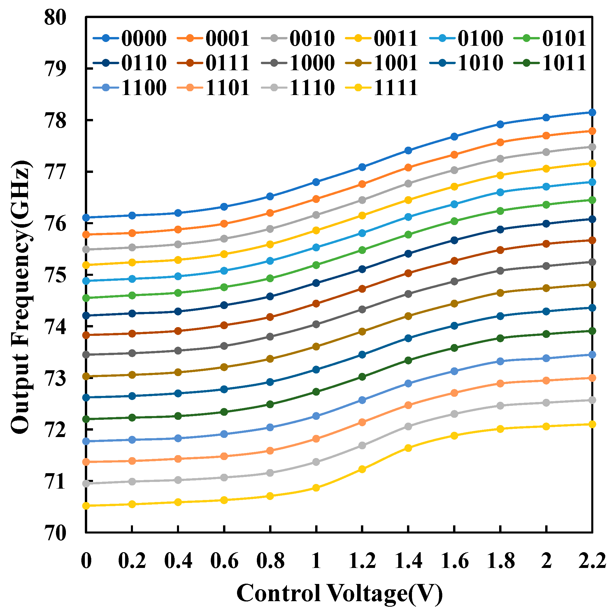
3. Results and Discussions
4. Conclusions
Author Contributions
Funding
Acknowledgments
Conflicts of Interest
References
- Le, V.H.; Duong, H.T.; Huynh, A.T.; Ta, C.M.; Zhang, F.; Evans, R.J.; Skafidas, E. A CMOS 77-GHz Receiver Front-End for Automotive Radar. IEEE Trans. Microw. Theory Tech. 2013, 61, 3783–3793. [Google Scholar] [CrossRef]
- Luo, T.-N.; Wu, C.-H.; Chen, Y.-J. A 77-GHz CMOS Automotive Radar Transceiver with Anti-interference Function. IEEE Trans. Circuits Syst. I Reg. Pap. 2013, 60, 3247–3255. [Google Scholar] [CrossRef]
- Cui, C.; Kim, S.-K.; Song, R.; Song, J.-H.; Nam, S.; Kim, B.-S. A 77-GHz FMCW Radar System Using On-Chip Waveguide Feeders in 65-nm CMOS. IEEE Trans. Microw. Theory Tech. 2015, 63, 3736–3746. [Google Scholar] [CrossRef]
- Vigilante, M.; Reynaert, P. A Coupled-RTWO-Based Subharmonic Receiver Front End for 5G E-Band Backhaul Links in 28-nm Bulk CMOS. IEEE J. Solid-State Circuits 2018, 53, 2927–2938. [Google Scholar] [CrossRef]
- Kalantari, M.; Shirinabadi, H.; Fotowat-Ahmadi, A.; Yue, C.P. A Single-Antenna W-Band FMCW Radar Front-End Utilizing Adaptive Leakage Cancellation. In Proceedings of the 2020 IEEE International Solid-State Circuits Conference Digest of Technical Papers, San Francisco, CA, USA, 17–21 February 2020; pp. 88–90. [Google Scholar]
- Hasch, J.; Topak, E.; Schnabel, R.; Zwick, T.; Weigel, R.; Waldschmidt, C. Millimeter-Wave Technology for Automotive Radar Sensors in the 77 GHz Frequency Band. IEEE Trans. Microw. Theory Tech. 2012, 60, 845–860. [Google Scholar] [CrossRef]
- Gao, L.; Wagner, E.; Rebeiz, G.M. Design of E- and W-Band Low-Noise Amplifiers in 22-nm CMOS FD-SOI. IEEE Trans. Microw. Theory Tech. 2020, 68, 132–143. [Google Scholar] [CrossRef]
- Ritter, P. Toward A Fully Integrated Automotive Radar System-on-Chip in 22 nm FD-SOI CMOS. Int. J. Microw. Wireless Technol. 2021, 13, 1–9. [Google Scholar] [CrossRef]
- Lin, Y.-S.; Chen, C.-C.; Lee, C.-Y. 7.2 mW CMOS Low-Noise Amplifier with 17.3dB Gain and 7.7dB NF for 76–77GHz Long-Range and 77–81GHz Short-Range Automotive Radars. Analog Integr. Circuits Sig. Process. 2016, 87, 1–9. [Google Scholar] [CrossRef]
- Murakami, T.; Hasegawa, N.; Utagawa, Y.; Arai, T.; Yamaura, S. A 9 dB Noise Figure Fully Integrated 79 GHz Automotive Radar Receiver in 40 nm CMOS Technology. In Proceedings of the 2019 IEEE Radio Frequency Integrated Circuits Symposium, Boston, MA, USA, 2–4 June 2019; pp. 307–310. [Google Scholar]
- Usugi, T.; Murakami, T.; Utagawa, Y.; Kishimoto, S.; Kohtani, M.; Ando, I.; Matsunaga, K.; Arai, C.; Arai, T.; Yamaura, S. A 77 GHz 8RX3TX Transceiver for 250 m Long Range Automotive Radar in 40 nm CMOS Technology. In Proceedings of the 2020 IEEE Radio Frequency Integrated Circuits Symposium, Los Angeles, CA, USA, 4–6 August 2020; pp. 23–26. [Google Scholar]
- Bameri, H.; Momeni, O. A High-Gain Mm-Wave Amplifier Design: An Analytical Approach to Power Gain Boosting. IEEE J. Solid-State Circuits 2017, 52, 357–370. [Google Scholar] [CrossRef]
- Park, D.-W.; Utomo, D.R.; Hong, J.-P.; Lee, S.-G. A 230–260 GHz Wideband Amplifier in 65nm CMOS Based on Dual-Peak Gmax-Core. In Proceedings of the 2017 IEEE Symposium on VLSI Circuits, Tokyo, Japan, 5–8 June 2017; pp. C300–C301. [Google Scholar]
- Singhakowinta, A.; Boothroyd, A. Gain Capability of Two-port Amplifiers. Int. J. Electron. 1966, 21, 549–560. [Google Scholar] [CrossRef]
- Chen, L.; Zhang, L.; Wang, Y.; Yu, Z. A Compact E-Band Power Amplifier with Gain-Boosting and Efficiency Enhancement. IEEE Trans. Microw. Theory Tech. 2020, 68, 4620–4630. [Google Scholar] [CrossRef]
- Heller, T.; Cohen, E.; Socher, E. A 102–129-GHz 39-dB Gain 8.4-dB Noise Figure I/Q Receiver Frontend in 28-nm CMOS. IEEE Trans. Microw. Theory Tech. 2016, 64, 1535–1543. [Google Scholar] [CrossRef]
- Guermandi, D.; Shi, Q.; Dewilde, A.; Derudder, V.; Ahmad, U.; Spagnolo, A.; Ocket, I.; Bourdoux, A.; Wambacq, P.; Craninckx, J.; et al. A 79-GHz 2×2 MIMO PMCW Radar SoC in 28-nm CMOS. IEEE J. Solid-State Circuits 2017, 52, 2613–2626. [Google Scholar] [CrossRef]
- Callender, S.; Pellerano, S.; Hull, C. An E-Band Power Amplifier With 26.3% PAE and 24-GHz Bandwidth in 22-nm FinFET CMOS. IEEE J. Solid-State Circuits 2019, 54, 1266–1273. [Google Scholar] [CrossRef]
- LaRocca, T.; Tam, S.-W.; Huang, D.; Gu, Q.; Socher, E.; Hant, W.; Chang, F. Millimeter-Wave CMOS Digital Controlled Artificial Dielectric Differential Mode Transmission Lines for Reconfigurable ICs. In Proceedings of the 2008 IEEE MTT-S International Microwave Symposium Digest, Atlanta, GA, USA, 15–20 June 2008; pp. 181–184. [Google Scholar]
- Murphy, D.; Gu, Q.J.; Wu, Y.-C.; Jian, H.-Y.; Xu, Z.; Tang, A.; Wang, F.; Chang, M.-C.F. A Low Phase Noise, Wideband and Compact CMOS PLL for Use in A Heterodyne 802.15.3c Transceiver. IEEE J. Solid-State Circuits 2011, 46, 1606–1617. [Google Scholar] [CrossRef]
- Wu, W.; Long, J.R.; Staszewski, R.B.; Pekarik, J.J. High-Resolution 60-GHz DCOs with Reconfigurable Distributed Metal Capacitors in Passive Resonators. In Proceedings of the 2012 IEEE Radio Frequency Integrated Circuits Symposium, Montreal, QC, Canada, 17–19 June 2012; pp. 91–94. [Google Scholar]


| Reference | [1] | [2] | [3] | [4] | [5] | This Work |
|---|---|---|---|---|---|---|
| Technology | 90 nm | 65 nm | 65 nm | 28 nm | 65 nm | 40 nm |
| Frequency (GHz) | 77 | 77 | 77 | 75 | 83 | 77 |
| Conversion Gain (dB) | 16 | 23 | 13 | 28 | 45 | 32 |
| Noise Figure (dB) | 13 | 14.8 | 7.95 1 | 8.3 | 15 | 11.83 |
| OP1dB (dBm) | −5 | N.A. | −13 | 3 | N.A. | −8 |
| DC Power (mW) | 28.5 | 27 | 25.8 | 77.3 2 | 120 3 | 32.4/132.7 3 |
| Chip Area (mm2) | 0.88 × 2.65 | 0.95 × 1.1 4 | 0.91 × 1.46 5 | 1.76 × 0.62 | 1 4 | 0.59 × 1 |
| Topologies (LNA/Mixer) | Single-ended/ Subharmonic | Single-ended/ Single-balanced | Single-ended/ Single-balanced | Differential/ Subharmonic | Differential/ Single-balanced | Differential/ Double-balanced |
Publisher’s Note: MDPI stays neutral with regard to jurisdictional claims in published maps and institutional affiliations. |
© 2021 by the authors. Licensee MDPI, Basel, Switzerland. This article is an open access article distributed under the terms and conditions of the Creative Commons Attribution (CC BY) license (https://creativecommons.org/licenses/by/4.0/).
Share and Cite
Cheng, S.; Li, L.; Mei, N.; Zhang, Z. A 77-GHz High Gain Low Noise Receiver for Automatic Radar Applications. Electronics 2021, 10, 1516. https://doi.org/10.3390/electronics10131516
Cheng S, Li L, Mei N, Zhang Z. A 77-GHz High Gain Low Noise Receiver for Automatic Radar Applications. Electronics. 2021; 10(13):1516. https://doi.org/10.3390/electronics10131516
Chicago/Turabian StyleCheng, Shuai, Linhong Li, Niansong Mei, and Zhaofeng Zhang. 2021. "A 77-GHz High Gain Low Noise Receiver for Automatic Radar Applications" Electronics 10, no. 13: 1516. https://doi.org/10.3390/electronics10131516
APA StyleCheng, S., Li, L., Mei, N., & Zhang, Z. (2021). A 77-GHz High Gain Low Noise Receiver for Automatic Radar Applications. Electronics, 10(13), 1516. https://doi.org/10.3390/electronics10131516