1. Introduction
In recent years, the advanced driver assistance system (ADAS) for automobiles has become a research hotspot and has made great development. The millimeter-wave radar has been a fundamental sensor in the ADAS due to its unparalleled adaptability to complex environments. Meanwhile, as the CMOS technology node scales, the CMOS millimeter-wave circuits and systems for radar applications become popular [
1,
2,
3,
4,
5] because of the high integrity and low cost. However, compared with the HEMTs and BJTs, CMOS transistors still suffer from low gain and high noise. Particularly, the RF front-end design of the long-range radar sensor based on CMOS technology faces more severe challenges since it requires better system sensitivity [
6].
For high system sensitivity, the receiver front-end is required to have a high amplitude gain and a low noise contribution. Many designs [
7,
8,
9,
10,
11] in CMOS technology for radar applications have been reported. Reference [
7] presents an LNA design with a gain of 20 dB and a noise figure (NF) of 4.6 dB. The receiver in [
8] achieves a conversion gain of 14 dB and an NF of 12.8 dB. The designs in [
7,
8] use the advanced FD-SOI technology, which means more cost for the consumers. Reference [
9] realizes an LNA with a gain of 17.3 dB and an NF of 7.4 dB using the microstrip lines as inductive components, which occupy more chip areas. References [
10,
11] adopt a passive mixer to realize a good NF of 9 and 8.7 dB, respectively. However, the LNA designs using the traditional neutralization technique have room for gain improvement.
This paper proposes a neutralization technique using an extra inductor based on the
Gmax theories in the gain-plane [
12,
13,
14]. Compared with the traditional capacitive neutralization technique, the proposed one helps the low noise amplifier (LNA) attain better gain and lower NF. The active mixer structure is also used to improve the gain. In order to reduce the contribution of flicker noise, the transformer coupling network is employed between the transconductance stage and the switch stage with a small DC current of the switching transistors. The receiver design has a high conversion gain and low noise figure, which is rather applicable for long-range radar applications.
Section 2 details the design of the LNA using the new neutralization technique, active mixer, and the design of the fundamental voltage-controlled oscillator (VCO) for LO signals of the mixer. The receiver measurement results and discussions, as well as performance comparison, are presented in
Section 3. The conclusions are drawn in
Section 4.
2. Receiver Design
The LNA is a critical block in the receiver front-end since it reduces the noise contribution of the following circuits and thus improves the system sensitivity. However, at millimeter-wave frequencies, the amplifiers in CMOS suffer from low gain. Especially, the parasitic capacitance,
Cgd, exacerbates the problem by providing a feedback path. Meanwhile, single-ended structures are significantly sensitive to the parasitics of the current return paths, particularly the parasitic inductive degeneration at the source terminal. Accordingly, differential amplifiers using the capacitive neutralization technique are mostly adopted to mitigate the above issues [
15,
16,
17,
18].
Unfortunately, according to the
Gmax theories in the gain-plane, the traditional neutralization technique is a sub-optimal method. References [
12,
14] give the maximum achievable gain in Equation (1), where
U expressed in Equation (2) denotes the unilateral gain or Mason’s gain, which is a real number. References [
12,
13] demonstrate a specific way using three inductors to realize the maximum gain in theory. However, the MOS transistors with the same gate and drain voltage cannot flexibly be configured for performance, and the main inductor becomes bulky at the lower frequencies. The LNA proposed to overcome the above issues is depicted in
Figure 1. An extra inductor
Ld is added to help attain the optimal design.
As described in [
12,
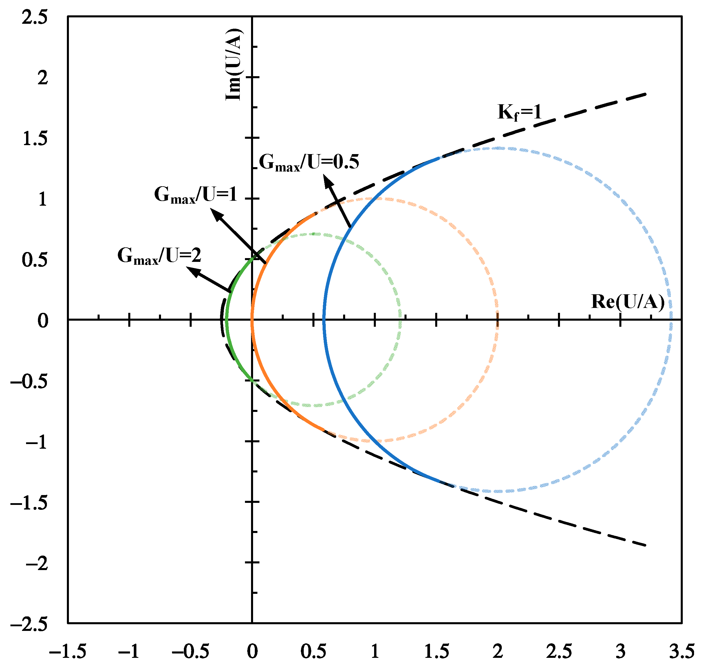
13], the maximum achievable gain of the gain cell is determined by the locations in the gain-plane shown in
Figure 2. A is the function of y-parameters shown in Equation (3), which is a complex variable. The
x-axis corresponds to the real part of the ratio of U to A, i.e., re(U/A). The
y-axis represents the imaginary part of the ratio of U to A. Some gain circles are illustrated, and the best location for achieving the maximum gain is marked, which approximately equals (−0.25, 0). The design with a ratio of U to A, which belongs to the points on the gain circles excluding the dot points, means its maximum achievable gain equals the corresponding gain. For example, the points in the gain circle of
Gmax/U = 2 make the amplifier attain a maximum gain of 2U. The parabola curve represents the stability boundary of K
f = 1. The stable region satisfying K
f > 1 is inside this curve. Meanwhile, the nearer the distance of the gain circle to the best location, the larger the maximum achievable gain.
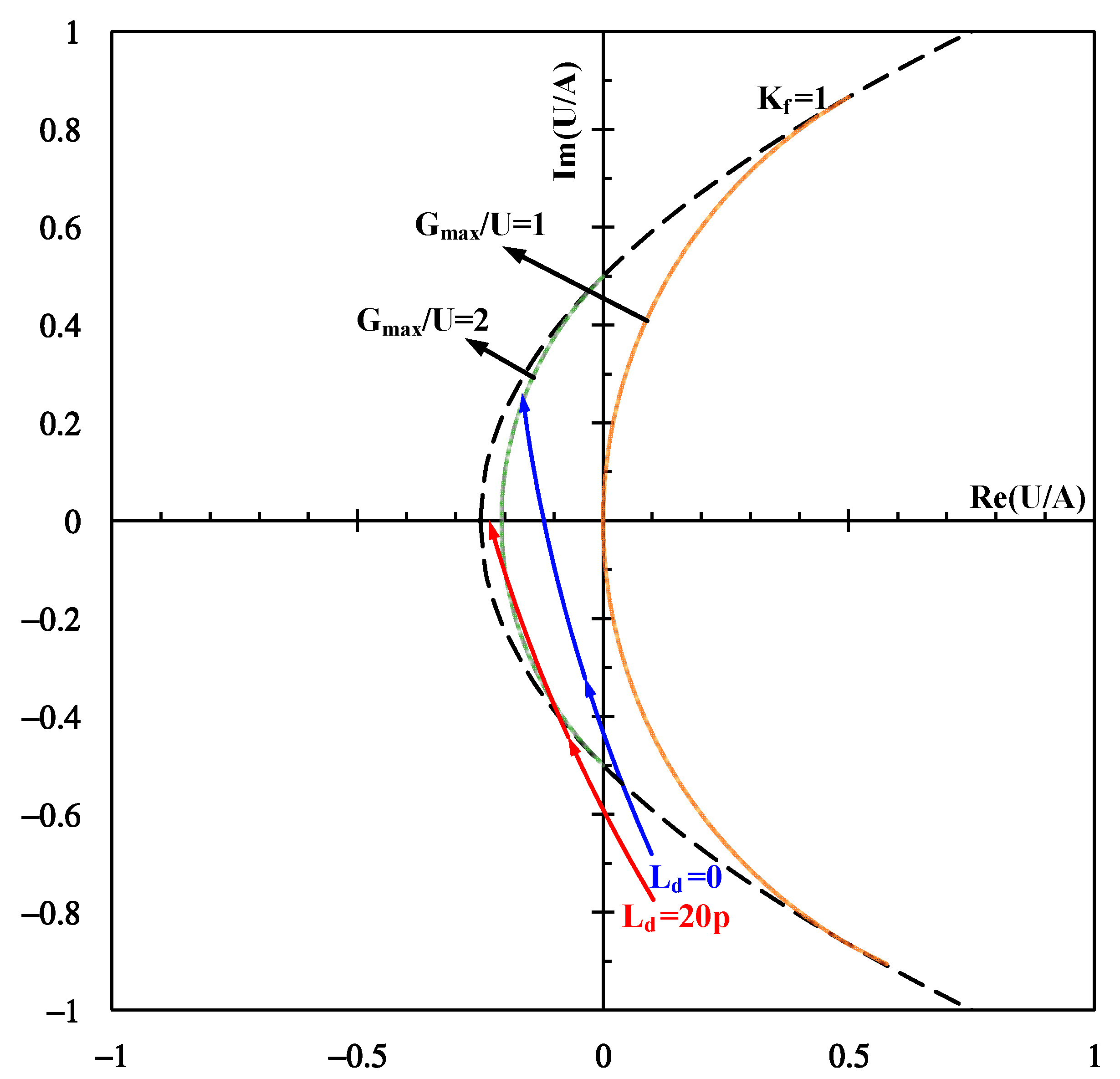
Figure 3 compares the location movements with increased capacitances between the proposed neutralization technique and the traditional neutralization technique. The blue trace exhibits the movements with increased neutralization capacitance of the traditional neutralization technique without
Ld. A larger capacitance helps the movements reach higher gain circles. However, the movement has a deviation from the best location, which means the amplifiers with the traditional neutralization technique are sub-optimal designs. The red trace demonstrates that an
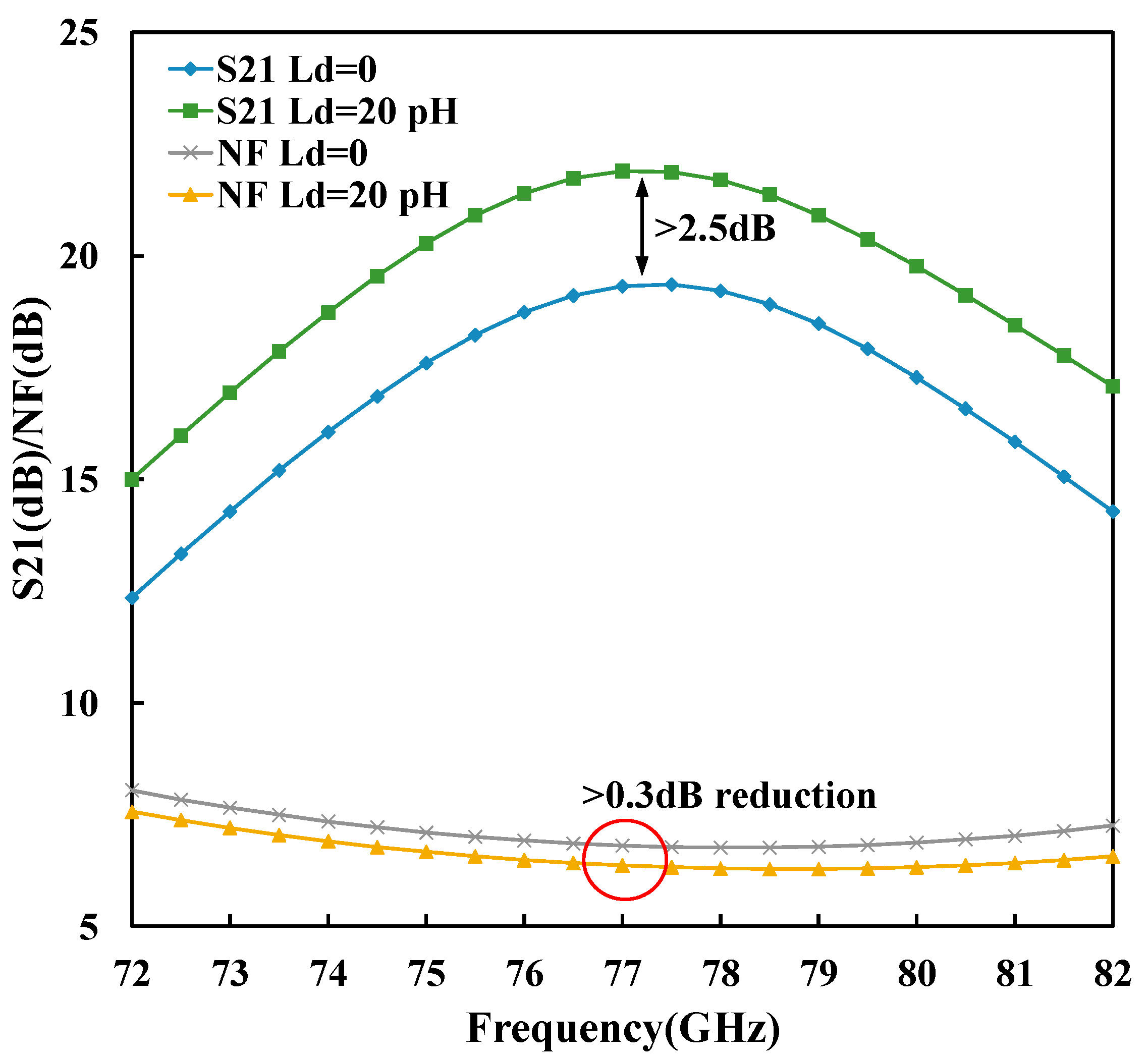
Ld of 20 pH helps the location move towards the best location more closely. To illustrate the performance improvements, the simulated S21 and NF of the LNA in
Figure 1 with
Ld = 0 and
Ld = 20 pH, respectively, are presented in
Figure 4. The results imply that
Ld contributes to higher gain and lower NF.
Therefore, the traditional neutralization technique adopts a large neutralization capacitance to obtain a high gain with a positive imaginary part of the U/A, which is a sub-optimal choice. The optimal neutralization technique adopts the appropriate neutralization capacitance and inductor, making a zero imaginary part of the U/A and the real part of the U/A close to −0.25, with the stable condition.
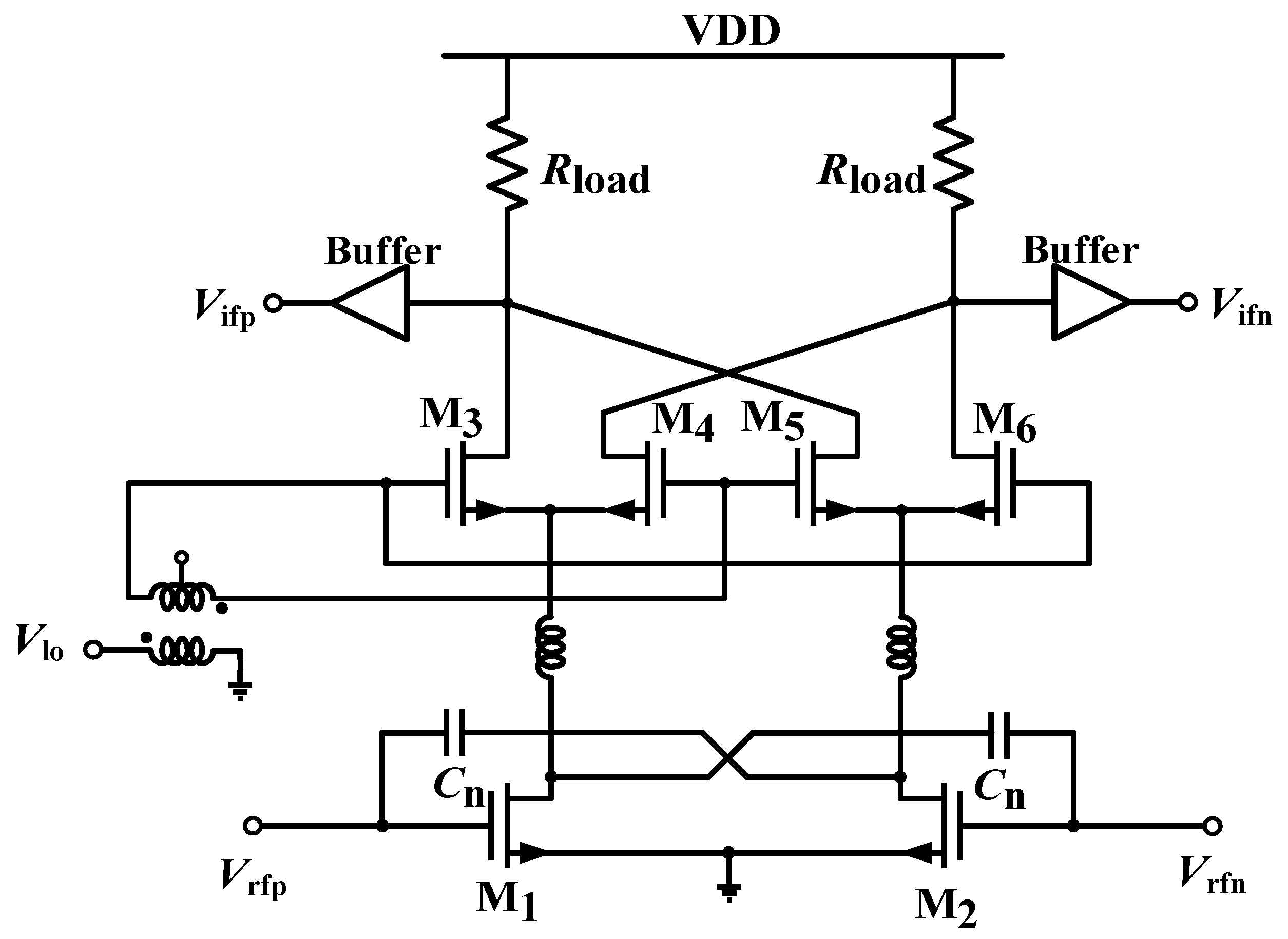
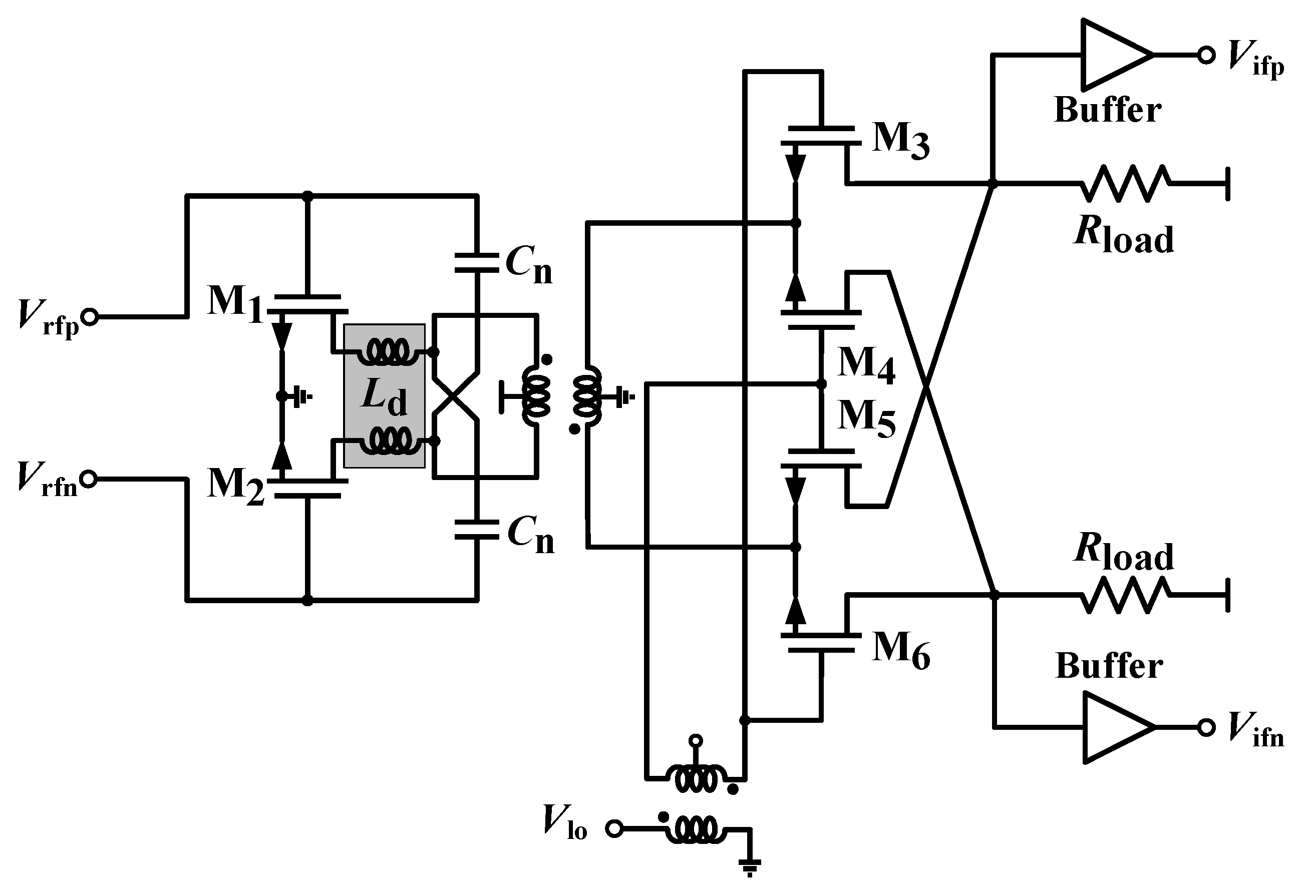
At the millimeter-wave frequency, to attain enough gain for the front-end, an active Gilbert mixer is utilized, which helps reduce the noise contribution of the subsequent blocks. However, the classic active mixer shown in
Figure 5 accompanied with high output flicker noise has difficulty achieving high gain due to the low voltage headroom across the load resistor. Therefore, we propose a high gain and low flicker noise mixer structure demonstrated in
Figure 6. The RF voltage signal is converted to RF current through the transconductance stage. Then the current signal is coupled to the switching stage by a 1:1 transformer. The DC current of the switching transistors is set to 0.25 mA, which greatly reduces the flicker noise contribution from the transistors. Meanwhile, high load resistors and the transconductance stage using the proposed neutralization technique help realize a high conversion gain. Another advantage of the proposed topology is the low amplitude level requirement of the LO signal.
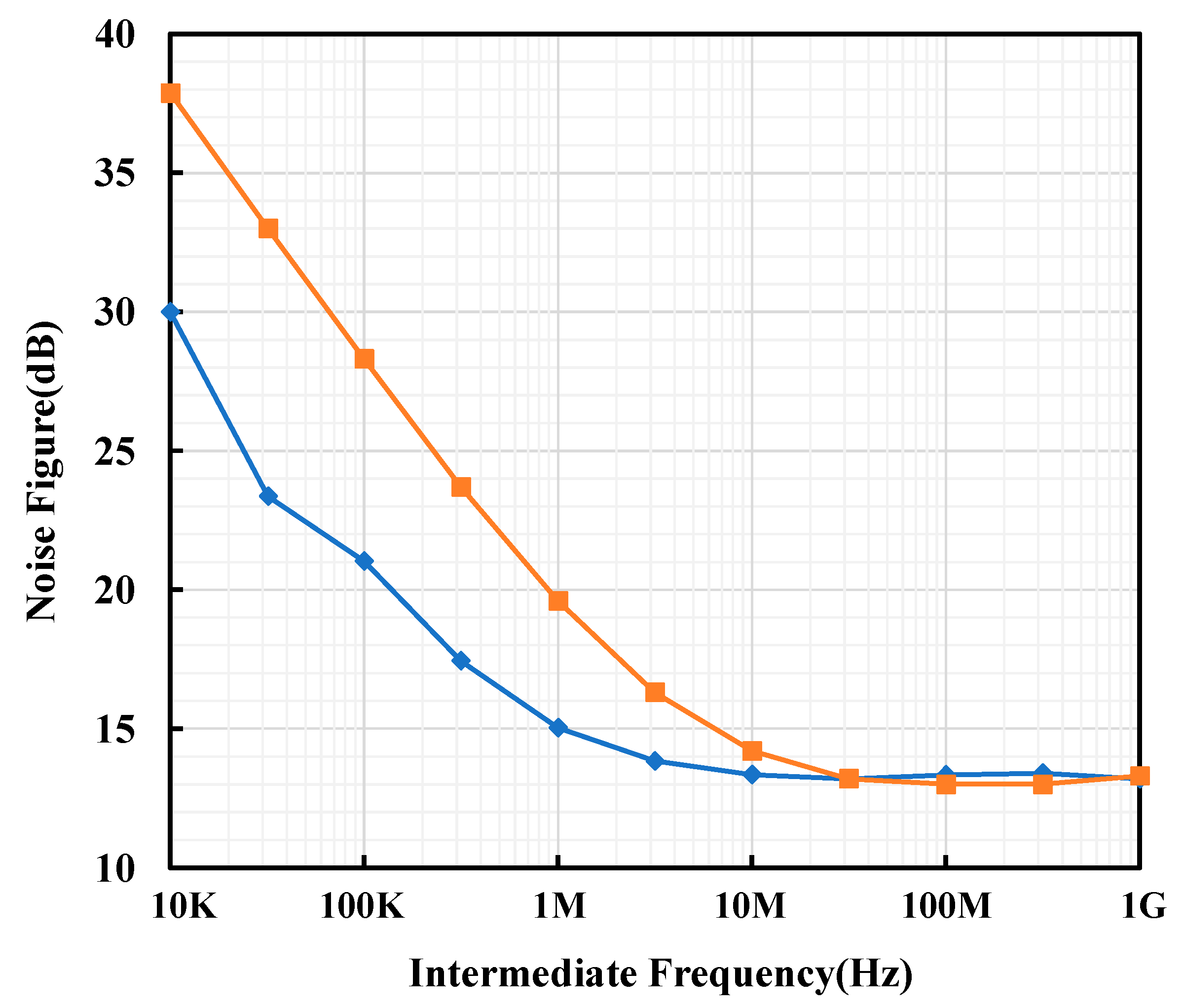
The NF comparison between the proposed mixer and the classic mixer is conducted to demonstrate the NF performance improvement. With a higher supply voltage, the classic mixer is designed with the same conversion gain of 11 dB as that of the proposed mixer. The simulated single-sideband (SSB) NF results are presented in
Figure 7. It is observed that the classic mixer design suffers higher NF at the flicker-noise regions and larger corner frequency compared with the proposed design. The NF of the proposed mixer is reduced by above 4 dB with the IF frequency lower than 1 MHz, which indicates the flicker noise contribution is significantly reduced.
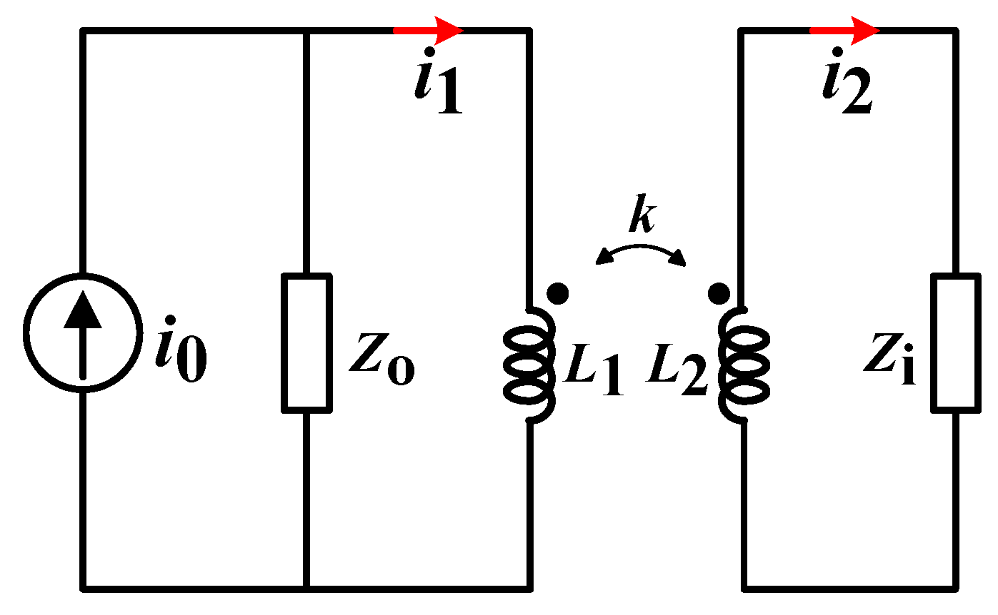
To simplify the gain analysis, the current coupling model is illustrated in
Figure 8. The current source
i0 represents the RF current converted by the transconductance stage.
Zo and
Zi denote the output impedance of the transconductance stage and the input impedance of the switching stage, respectively. According to the principle of the transformer, we obtain Equations (4) and (5). The current coupling factor provided by the transformer is derived as Equation (6). Therefore, the overall gain can be obtained from Equation (7). It is apparent that a larger |
k| results in a larger numerator and a smaller denominator. So, a larger coupling factor is beneficial for the conversion gain. The structure of the stacked transformer is a proper choice. The transformer design in the commercial Electro-Magnetic simulator HFSS (i.e., High Frequency Structure Simulator) is presented in
Figure 9.
Figure 10 demonstrates the inductances of the primary and secondary windings and the coupling factor, k, between them. At 77 GHz, a large k of −0.83 is realized in the transformer design. Meanwhile, the quality factors are higher than 9 at the desired frequencies.
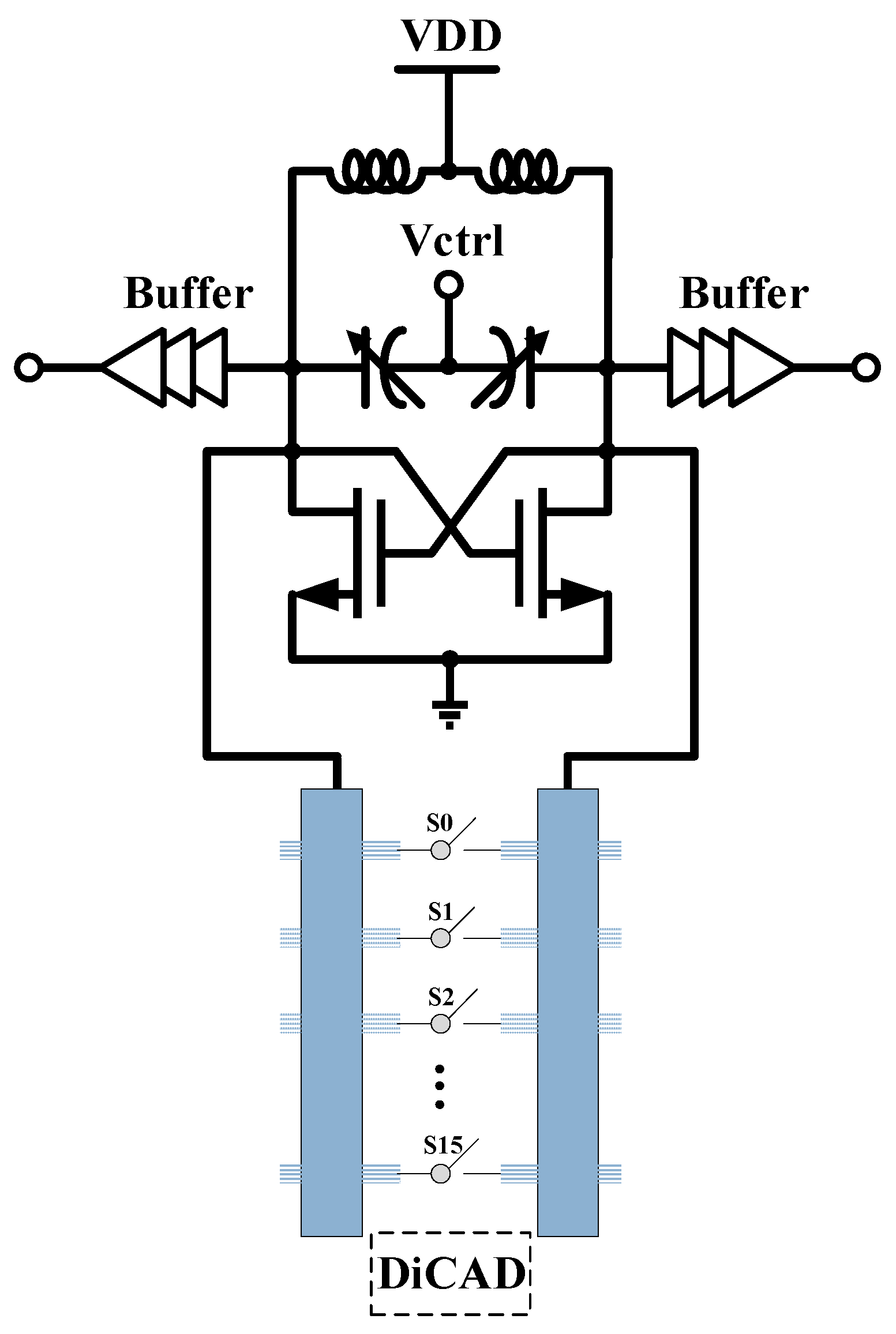
In addition, an on-chip 77 GHz fundamental VCO is realized for the LO signal, as shown in
Figure 11. Small varactors with minimal length to reduce tank loss are employed for continuous frequency tuning. At the millimeter-wave frequencies, the digitally controlled artificial dielectric (DiCAD) structure is widely adopted [
19,
20,
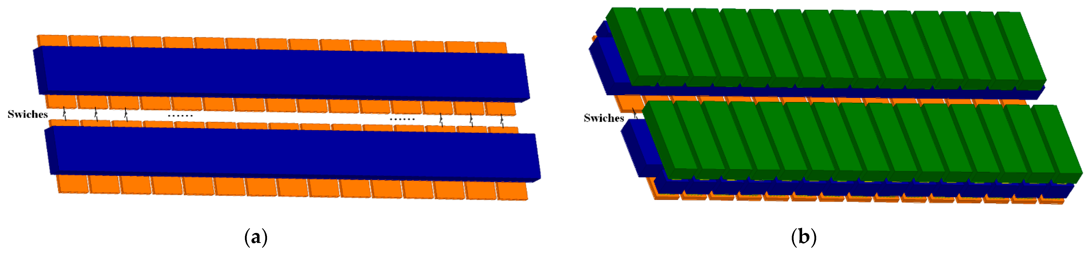
21] for discrete frequency tuning because it is easy to model and introduces less parasitic inductance for the capacitor bank. The traditional DiCAD structure is shown in
Figure 12a. According to Equation (8), the differential open transmission lines behave like a capacitor, whose capacitance is controlled by the digital switches. The traditional DiCAD structure suffers from a limited capacitance range. Therefore, to make the VCO adapt to process-voltage-temperature (PVT) variations better, the proposed DiCAD structure with double-stacked slots presented in
Figure 12b is utilized.
From the view of the minimum capacitance cell, the proposed DiCAD structure doubles the capacitance,
Con, when the switch is on, while the capacitance,
Coff, is just increased a small amount with the switch off. The two structures are simulated by HFSS and the spectre simulator to get the results of capacitance increments and quality factors demonstrated in
Figure 13. The DiCAD structure is controlled by the 4-bit switch word, where the high voltage level switches on the corresponding control transistor. The conventional structure achieves a capacitance range from 42 to 59 fF, while the proposed one realizes the range from 38 to 63 fF. The amount of capacitance increment is increased from 17 to 25 fF, which is 42% bigger, using the proposed structure. The minimum quality factor is decreased from 14.4 to 12.6 with all switches on, which is a slight deterioration.
3. Results and Discussions
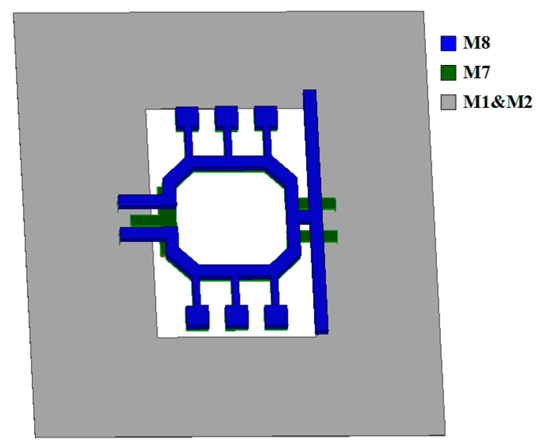
This receiver is designed in HLMC 40-nm technology with 8 layers of metals. The top metal, M8, has a thickness of 3.3 μm, and the thickness of M7 is 0.8 μm. The maximum oscillation frequency, fmax, of the MOS transistors with the minimum channel length of 40 nm is about 230 GHz. The passive components in the full layout, like inductors, interconnecting lines, and transformers, are divided into three parts, which are imported in HFSS to conduct the E-M simulations, respectively. The ground plane consists of M1 and M2 for less loss. The active transistors are extracted with parasitic resistances and capacitances by the StarRC tool for the fully post-simulations.
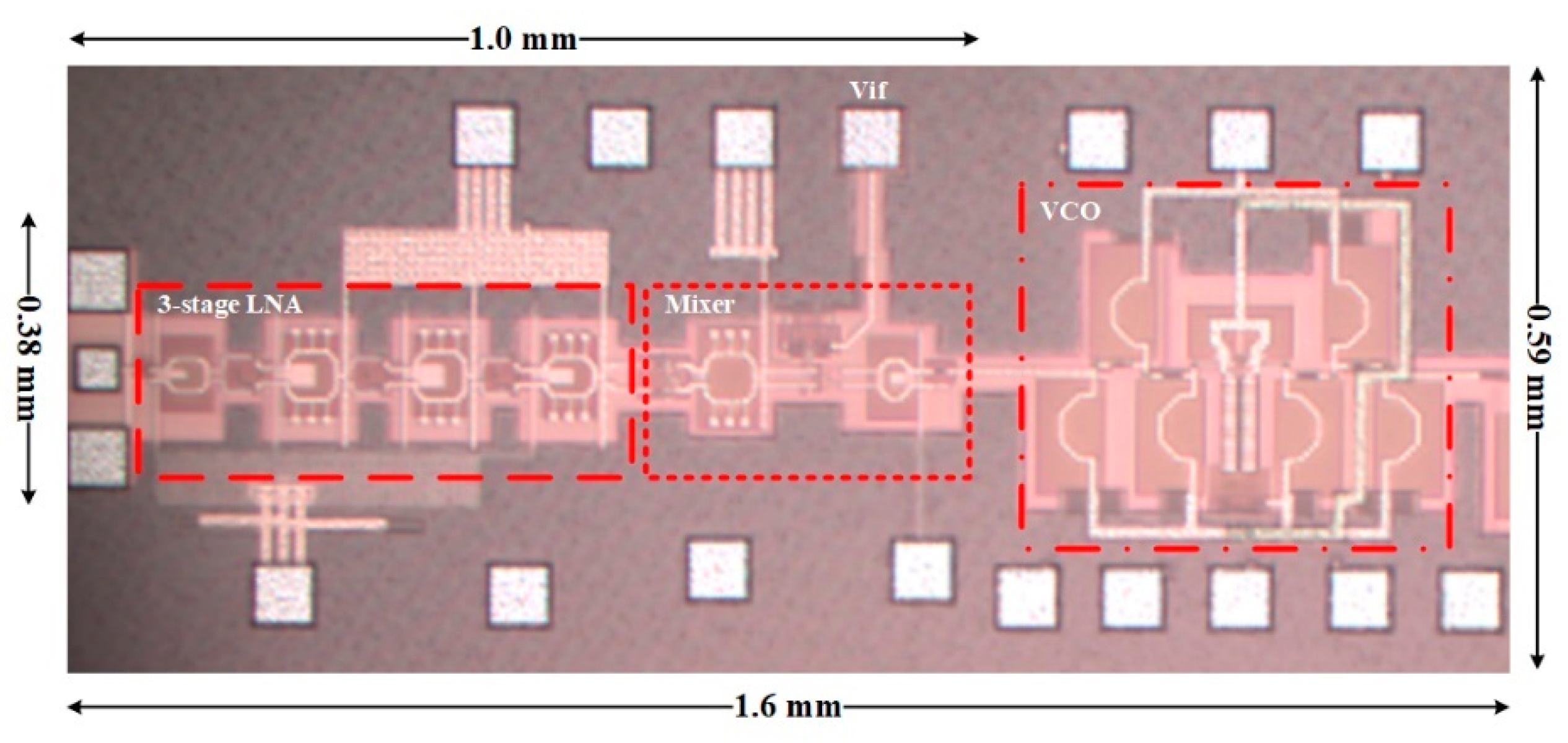
The receiver’s chip photograph is shown in
Figure 14. The LNA and mixer occupy a core area of 1 × 0.38 mm
2, while the size of the VCO is 0.59 × 0.59 mm
2. The LNA consumes a DC power of 24 mW from a 0.8-V supply, and the mixer consumes 9.2 mW from a 1.2-V supply. The core of the VCO circuit dissipates 33 mW from a 1.2-V supply.
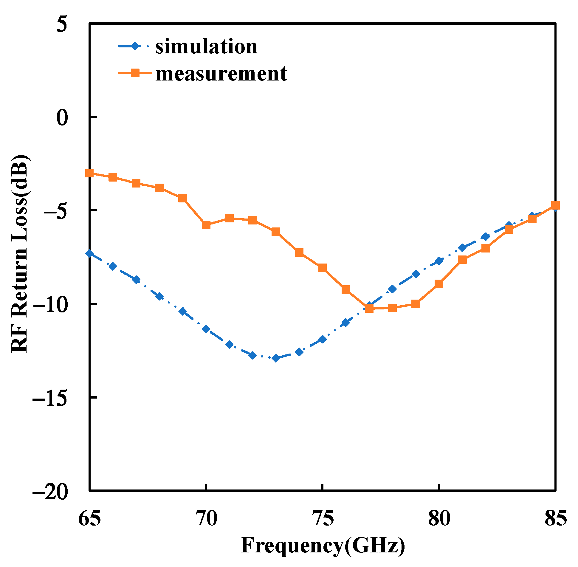
With the network analyzer, the input return loss is measured, as shown in
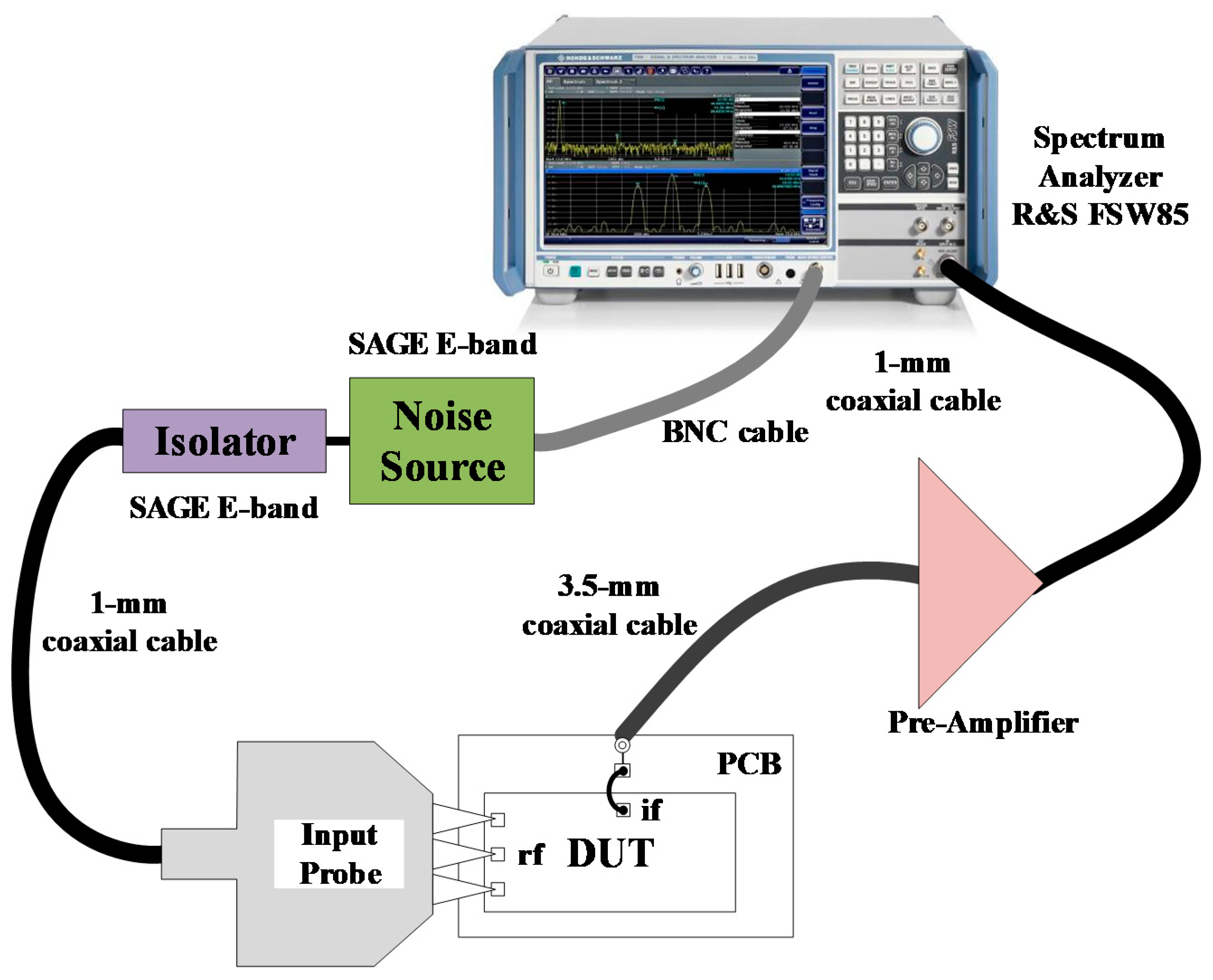
Figure 15. It is observed that the measured S11 has a deviation to higher frequencies. The deviation mainly results from the transistor model inaccuracy in high frequencies. The RF signal is provided by a signal source and a 6× frequency multiplier, while the on-chip VCO offers the LO signal. The measurement setup of the NF is depicted in
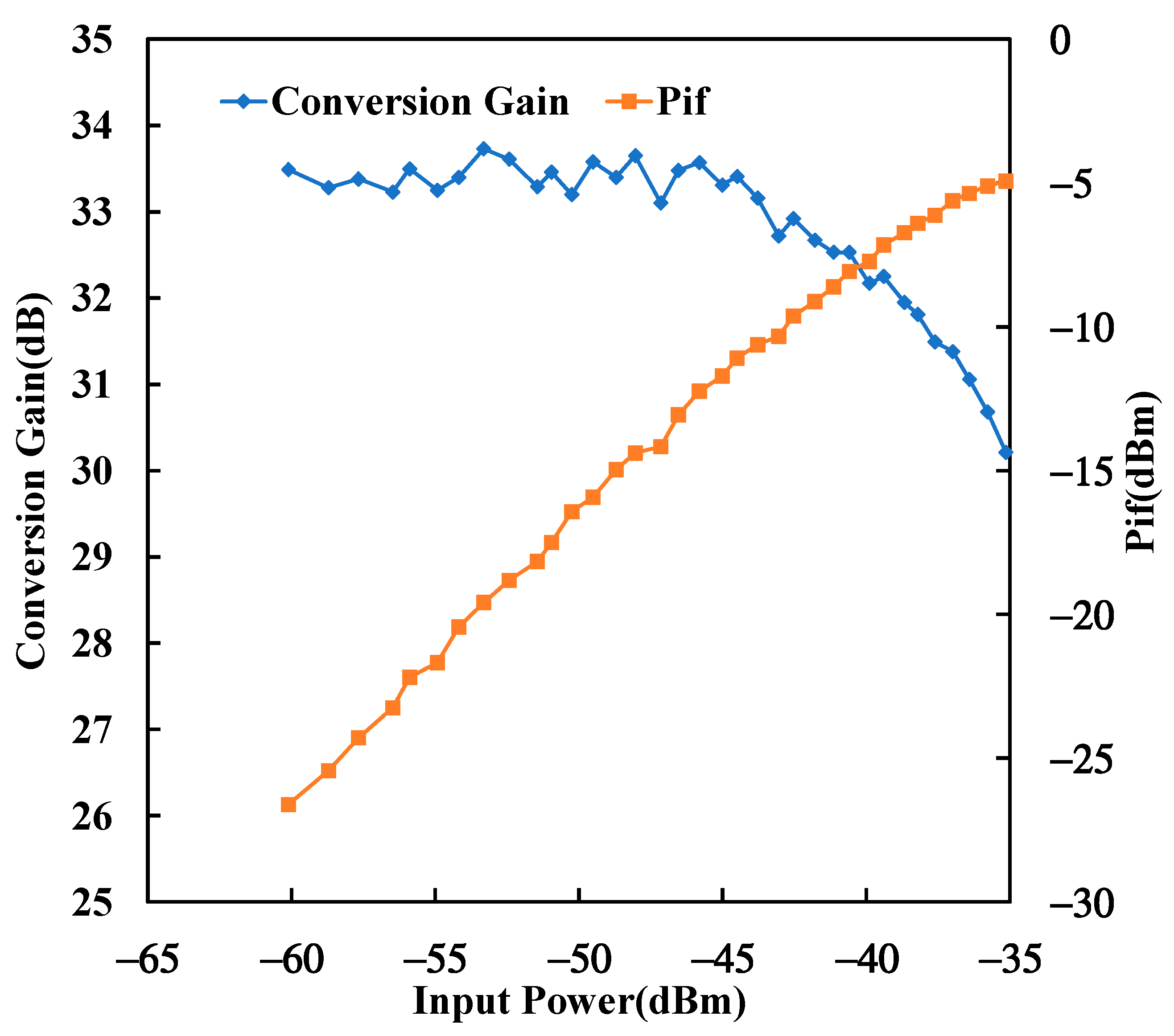
Figure 16, in which a SAGE E-band noise source is utilized. The conversion gain and SSB NF results of the receiver with IF = 1 GHz are demonstrated in
Figure 17. The buffer loss, about 3.5 dB, is de-embedded. Then, a maximum conversion gain of 34 dB and a minimum NF of 10.66 dB are obtained. At 77 GHz, the achieved conversion gain and SSB NF are 32 and 11.83 dB. The measurements are generally consistent with the simulation results. Due to the model inaccuracy in the desired frequencies, the conversion gain has a peak at a higher frequency. Correspondingly, the minimum NF of 10.66 dB is realized at the same frequency; some NF deviations relate to the input impedance deviations. Additionally, the measured OP1dB at 77 GHz is about −8 dBm, as shown in
Figure 18.
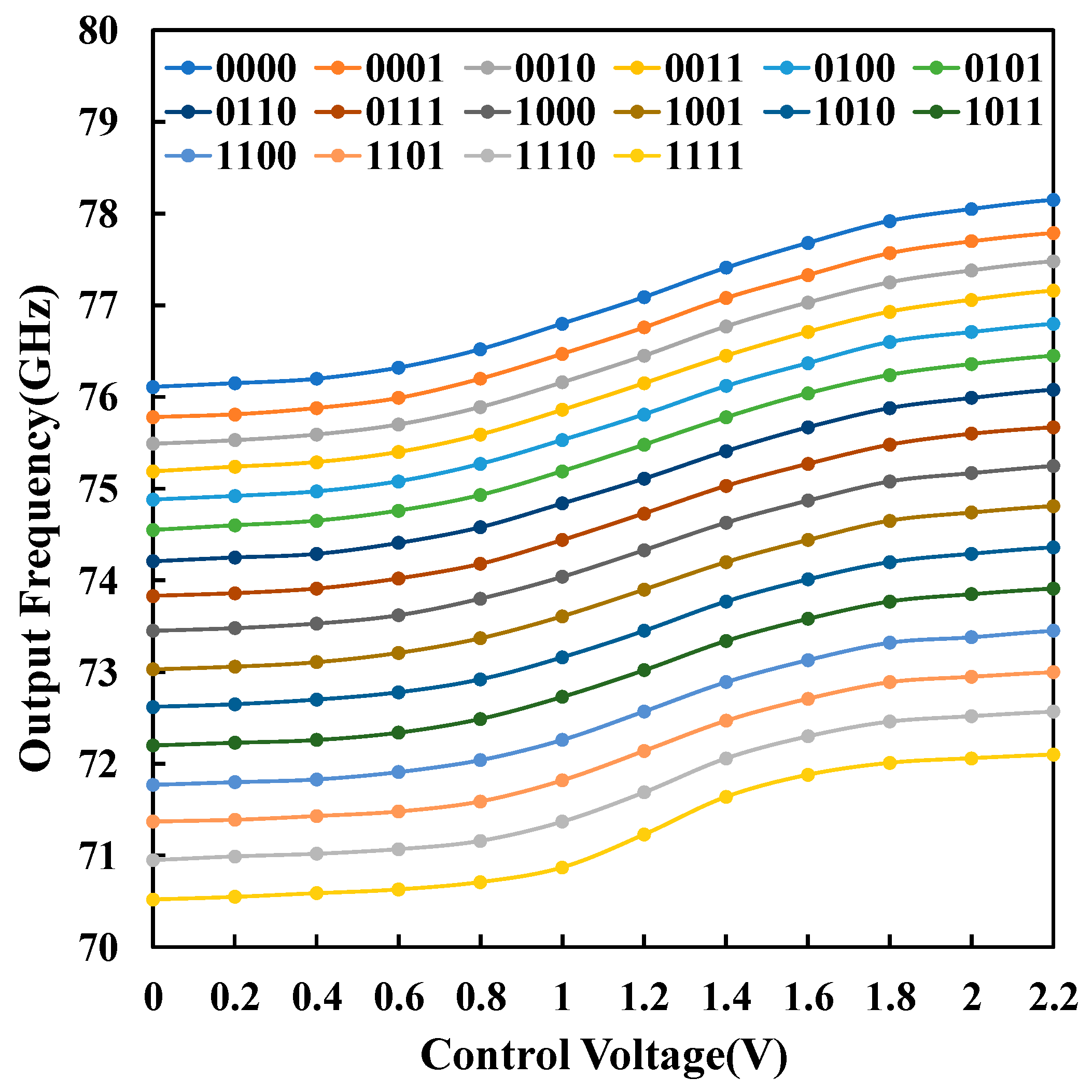
The VCO is measured by the spectrum analyzer FSW85. A tuning range from 70.5 to 78.2 GHz, i.e., a 10.4% fractional range, is achieved, as shown in
Figure 19. Meanwhile, the phase noise at 1 MHz offset frequency is −91.8~−93.48 dBc/Hz, and the phase noise of 77.74 GHz is shown in
Figure 20. The phase noise measurements are bigger than the simulated results by 1~2 dB.
The performance comparison of the receiver with other designs is shown in
Table 1. This work achieves a relatively high conversion gain and a relatively low NF. The high gain and low noise receiver is applicable to the long-range radar sensor.


