Article

Efficient Directional Antenna Design Suitable for Ubiquitous Power Internet of Things

1
Yunnan Innovation Institute·BUAA, Kunming 650233, China
2
School of Electronic and Information Engineering, Beihang University, Beijing 100191, China
3
Joint War College, PLA National Defense University, Beijing 102249, China
*
Author to whom correspondence should be addressed.
Electronics 2021, 10(13), 1521; https://doi.org/10.3390/electronics10131521
Submission received: 11 May 2021 / Revised: 7 June 2021 / Accepted: 12 June 2021 / Published: 23 June 2021
(This article belongs to the Section Microwave and Wireless Communications)

Abstract

:
Today’s power systems are developing from traditional multi-sensor systems to ubiquitous power Internet of Things systems. The environmental backscatter technology makes communication equipment get rid of the dependence on power supply, is more energy-efficient, and effectively extends the communication distance, which is very suitable for power Internet of Things scenarios. Tag antenna is an important part of environmental backscattering, but it has problems such as low reliability and insufficient reading distance in the traditional power Internet of Things. In view of the above problems, this paper designs a double-antenna structure tag antenna, which adopts omnidirectional receiving and directional transmitting methods to achieve the purpose of comprehensive signal coverage for the power Internet of Things application scenarios. It has the characteristics of obvious gain, small side lobe, and strong anti-interference.

1. Introduction

Internet technology and new energy technology will promote a new round of energy revolution. The combination of smart grid and “Internet +” technology has become a current research hotspot in the field of electrical engineering. The concept of the Internet of Energy and the Ubiquitous Power Internet of Things (UPIoT) has emerged [1]. The construction of smart grids has expanded a broader space for development. Among them, the Internet of Things technology, as a current hot technology in the field of science and technology, has broad prospects for its application in the power field. In order to further realize the goal of the smart grid, the power system must make good use of the Internet of Things technology in the 5G era to promote the diversified development of the power system from the traditional power grid to the smart grid, so as to better meet the needs of social development [2].
Due to the explosive growth in the number of power grid equipment, unified identification technology has become the data foundation for the deepening application of the power Internet of Things [3]. At present, smart grids have used QR codes and radio frequency identification (RFID) to uniformly identify equipment, tools and other assets. RFID technology started in the 1980s, using the spatial electromagnetic field coupling of radio frequency signals to achieve the purpose of non-contact automatic identification and information transmission between tags and readers [4]. However, the traditional backscatter technology has three main limitations: the activation of the backscatter transmitter relies on an external power source, it only responds passively when the reader interrogates, and it is susceptible to the influence of adjacent active readers. Therefore, environmental backscattering is proposed to assist wireless power communication.
In order to solve the problem that the communication distance of the RFID tag is limited by the signal coverage of the reader, the academic community proposed the dual-site backscatter technology in 2013 [5]. In 2014, a turbocharged environment backscatter system with a multi-antenna elimination design and a new encoding mechanism was adopted to improve the communication rate and range [6]. In 2015, the BackFi system proposed by academia significantly improved the WiFi backscattering system, using full-duplex technology to backscatter the WiFi signal in the environment to enable long-distance communication between the sensor and the relay node [7]. In 2016, frequency-shift backscattering transferred the carrier signal to adjacent non-overlapping frequency bands to achieve stronger decoding and achieve 802.1b transmission, which can be more energy-efficient than traditional WiFi, to prove that environmental backscattering is in typical mobile and practicality in static sensing scenes [8].
In addition, a new fully asymmetric backscatter communication protocol, a new sensor structure of the backscatter platform, and a low-power backscatter system using commercial WiFi are also proposed. At present, the University of Washington has verified the feasibility of this technology through experiments [9]. In 2019, academia proposed a single-base backscattering communication system using continuous interference cancellation, in which a single reader simultaneously serves multiple backscattering tags or nodes (BNs) [10]. In 2020, with the development of intelligent transportation technology and vehicle road cooperation technology, it has important application value to add the label recognition function of roadside traffic signs to the forward collision avoidance radar through the backscatter communication technology. Based on the traditional automobile collision avoidance radar, a backscatter communication system of frequency modulated continuous wave radar based on spread spectrum coding is proposed [11].
The tag antenna is an important part of the environmental backscatter. The tag antenna is a radio frequency signal transceiver that connects the electronic tag and the reader. It radiates the radio frequency signal output by the tag into the space in the form of electromagnetic waves, and at the same time, receives and stores the radio frequency signal from the reader [12]. The working frequency of the sub-tag and the electrical parameters of the antenna determine the type of the tag antenna, and are affected by factors such as the radio frequency characteristics of the tag attachment and the metal objects deployed around it. The working frequency bands of microwave electronic tag antennas are concentrated in 800 MHz~900 MHz, and 2.45 GHz and 5.8 GHz, using electromagnetic wave propagation coupling [13]. Among them, the signals in the environment used by environmental backscattering are generally 400–600 MHz TV signals, 2.4 GHz WiFi and 4G and 5G signals, so they belong to microwave tag antennas.
However, there are some problems when the traditional microwave electronic tag antenna is directly applied in the electric Internet of Things environment. First, the label communication distance is short. The reading distance of traditional RFID technology is less than 5 m. In typical electric power Internet of Things scenarios, due to the safety distance requirement of live operation and the limitation of some remote and steep terrain, the identification distance of the device tag is usually 20–200 m [14], which is difficult to meet with the existing technology. Secondly, label reliability is low. Tags may be damaged and data lost in the strong electromagnetic environment. At the same time, by the electromagnetic environment around the passive induction, the label is frequently misstarted and shortens the life [15]. Finally, the label fetching energy is unstable. Tag fetching has certain requirements on angle and density. In some scenarios, the close paste of labels leads to too close distance and certain interference between each other when reading, which will result in reading failure or a too long time [16]. Label paste position has a certain occlusion and will also lead to read failure [17]. In order to solve the problems existing in the current traditional tag antenna in the electric Internet of Things environment, we designed a high-performance tag antenna with miniaturization, orientation, high gain and narrow band characteristics by selecting appropriate substrate material and antenna structure and optimizing it.
The main contributions of this paper include: (1) designing a tag antenna that meets the requirements of omni-directional reception and directional transmission in the 5G environment; (2) proposing the selection and improvement method of antenna structure; (3) adopting a multi-objective genetic algorithm for antenna optimization. Through detailed performance evaluation, this research shows that the proposed tag antenna can meet the expectations of the intelligent power Internet of Things.
The rest of this article is organized as follows. Section 2 introduces the backscatter communication system of the power Internet of Things. Section 3 explains the structure selection of the antenna and the optimization process of the algorithm. Section 4 gives numerical results to prove the advantages of our antenna. Finally, Section 5 summarizes the full text.

2. Backscatter Communication System for Power Internet of Things

The power Internet of Things uses the power information communication network to realize the efficient transmission, analysis, and processing of smart terminals and equipment information on all links of the power grid, thereby further improving the depth and breadth of smart grid information perception, power system analysis, early warning, self-healing, and disaster prevention [18]. The ability of power grids and the level of safe operation of the power grid can realize the refined management of power from production to consumption, as well as achieve the goals of energy saving and consumption reduction, as shown in Figure 1. Among them, the unified identification access and intelligent edge computing of the perception layer are the foundation of the power Internet of Things [19].
At present, the State Grid Corporation of China has used QR codes and RFID to uniformly identify equipment, tools and other assets, and uses backscatter technology to communicate with mobile gateways [20]. However, it has been found to have low reliability and short service life in practical applications. In addition, there are problems of energy consumption and path loss, and the communication distance is greatly shortened. The short communication distance of the tag is also a large problem [21]. The 5G signal has a shorter wavelength and is closer to the straight line of light. In the scene shown in Figure 2, in the power system, some equipment has to be placed in a more precarious environment due to the natural environment, and is more likely to be blocked by obstacles. Traditional tags do not have the function of a radio frequency reflector and cannot bypass obstacles through reflection [22].
The reading distance of traditional RFID technology is no more than 5 m [23]. However, considering the requirements of the safe distance for live working in the power Internet of Things scene and the restrictions of some steep terrain, the identification distance of the device tag is usually 20–200 m [24]. To solve this problem, we adopt a passive dual antenna system.
The basic data acquisition equipment belongs to omni-directional transmission and omni-directional reception, but when the tag antenna is arranged in the power Internet of Things system, only the receiving antenna needs to cover as much omni-directionally as possible to collect the signals in the environment, and then use the transmitting antenna to read legally. The position of the device is forwarded. Therefore, the antenna system adopts an omnidirectional receiving and directional transmitting structure. Next, we will design the transceiver antenna of the RF reflector.

3. Antenna Structure and MOGA Optimization

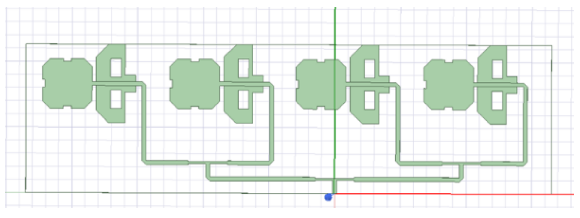
3.1. Receiving Antenna Structure

Considering that the receiving antenna needs to receive signals from the environment in an almost omnidirectional way, the receiving antenna first chooses the four-element microstrip antenna. Four-element microstrip antenna belong to the standing wave patch antenna—a microstrip antenna radiating element only on one side of the media, or coaxial feed microstrip line can be used in the design of this article. The back of the receiving antenna are linked together and integrated into a plane, with the microstrip line feeding and resonant input resistance being very big, needing 50 Ω transmission line impedance matching. The matching can be carried out by selecting the appropriate feeding position and considering the influence of the selection of the position on the antenna radiation characteristics.
In the first version of the program design, the most basic rectangular patch was first selected for simulation, and the coaxial probe was used to feed power. According to the empirical formula of patch size calculation in literature [25], the initial length W, width L and the position of the feeding point of the patch can be calculated. Taking into account the mutual coupling effect between the patch units, the unit pitch is taken as 0.5 λ g ~ λ g .
The four-unit rectangular patch antenna array is fed in parallel through 1–4 power dividers, and the input end is at the same distance from each unit and fed in the same phase. The model is shown in Figure 3.
The directional pattern function of the microstrip array antenna is composed of the directional function of the basic element antenna and the array factor of the constant-amplitude and in-phase continuous array of length L. Due to the narrow frequency band of the microstrip antenna, it cannot cover a large number of signals existing in the environment such as 5G signals at the same time [26]. Therefore, the bandwidth of the microstrip antenna needs to be further improved, resulting in the second structure of the receiving antenna. There are many ways to broaden the frequency band of a microstrip antenna. Due to the shape of the patch affecting the bandwidth, the patch and the floor are often grooved or cut to change the shape of the patch. According to Formula (1), the width L of the high-efficiency rectangular radiation patch is designed:
L = c 2 f 0 ε e 2 Δ L ,
In addition, the impedance bandwidth conversion formula can calculate the 50 Ω input impedance corresponding to the width of the bottom of the microstrip line W g = 3 mm, by cutting off an isosceles triangle on each of the four corners of the rectangular patch, and cutting off a rectangle on each of the top, left and right sides to achieve a gradual effect [27]. In order to extend the bandwidth, the upper two corners of the grounding plate were cut, and two symmetrical rectangular slots were opened on the grounding plate. In addition, two rectangles are cut under the grounding plate to reduce the floor space of the grounding plate. The broadband microstrip antenna unit model is shown in Figure 4.
In the antenna design process, by changing the position and size of the cut triangle, the size of the rectangular slot on the grounding plate, and the length of the grounding plate, the matching of the antenna bandwidth and performance was improved. In order to prevent the antenna performance from deviating too much, the upper and lower limits of the parameter floating are controlled within a small range during adjustment. The size of the antenna after the structural improvement is shown in Table 1. The improved four-element patch antenna structure is shown in Figure 5.

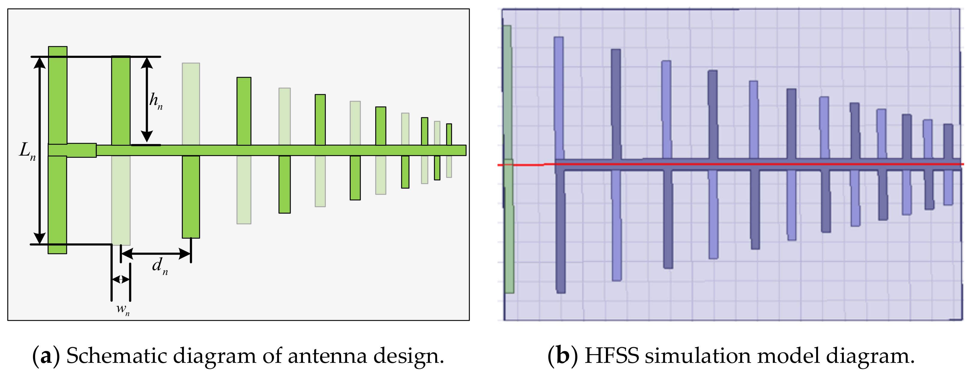
3.2. Transmitting Antenna Structure

Due to the transmitting antenna being a directional antenna, an end-fire antenna such as a log-period dipole antenna is first considered [28]. The log-period dipole antenna (LPDA) is a broadband linearly polarized antenna. In order to make the tag structure more concise, a plane printing structure is adopted to integrate the transceiver antenna on a plane. For the transmitting antenna, the log-periodic antenna is a directional end-fire antenna with a wide frequency band. However, in order to cover point-view signals, WiFi, 4G, and 5G signals in the environment as much as possible, the antenna bandwidth needs to be further extended. Therefore, the log-period antenna still has room for improvement.
It is known from the antenna analysis theory that attaching to the logarithmic period can effectively change its appearance and expand a wide antenna array. The antenna structure is shown in Figure 6. The length of the antenna element is denoted by L n , and the extension of the end of each antenna element intersects at a point, called a virtual vertex, and the opening angle is α . Denote the vertical distance from the virtual vertex to each antenna element as R n , the width of the element as W n , and the distance between two adjacent elements as d n . The original dimensions of the log-periodic antenna are shown in Table 2.
The geometric structure of the antenna is determined by the geometric factor τ and the spacing factor σ:
τ = R n + 1 R n = L n + 1 L n = d n + 1 d n ,
σ = d n 4 h n ,
The number of antenna elements can be obtained by the following formula:
N a = 1 + lg ( K 2 / K 1 ) lg τ ,
Among them, K1 and K2 are cutoff coefficients:
K 1 = 1.01 0.519 τ ,
K 2 = 7.10   τ 3 21.3   τ 2 + 21.98   τ 7.30 + σ ( 21.82 66   τ + 62.12   τ 2 18.29   τ 3 ) ,
In addition, it is also necessary to estimate the width of the vibrator:
Z a 120 log e ( h / a ) 2.25 ,
LPDA is a directional end-fire antenna, and the maximum radiation direction is from towards the short dipole end [29]. Generally speaking, the larger the value, the greater the number of oscillators in the radiation area, the stronger the directivity of the antenna, and the smaller the half-power angle of the pattern. The length of the longest vibrator and the shortest vibrator of LPDA determines its operating frequency [30].
The final antenna structure consists of a broadband microstrip antenna array and a log-period dipole antenna, as shown in Figure 7. Both antennas are broadband antennas, and the frequency meets the 5G signal requirements. The microstrip antenna array is responsible for receiving signals in the environment and forwarding them through a log-periodic antenna [31], and there are fewer side lobes. Since the feed end of the log-periodic antenna is at the short end, it cannot be directly connected. It is necessary to connect the feed network of the microstrip array to the feed end of the log-periodic antenna through a coaxial line.

3.3. MOGA Optimization

This paper adopts NSGA-II genetic algorithm and introduces the concept of Elitism. On the basis of traditional genetic algorithm, a non-dominant sorting process is added, that is, the parent and offspring are mixed and then sorted and selected to prevent the loss of outstanding individuals from the parent [32]. At the same time, in order to maintain the diversity of the population, density estimation and comparison operators are used in the selection of the binary tournament to effectively prevent local convergence [33]. Therefore, this article makes the above selection, and the algorithm flow chart is shown in Figure 8.
Due to the structure of the log-period dipole antenna being more complicated, the MOGA algorithm is used to optimize the transmitting antenna, therefore, we select the length, width and spacing of the vibrator as the variables to be optimized. In the antenna design process, the gain, bandwidth, and side lobes of the antenna are important indicators to measure the performance of the antenna, so the functions corresponding to the above three indicators are defined as the objective function.
A multi-objective optimization problem with 3 decision variables and 3 objective functions can be expressed as:
o p t i m a l f ¯ ( x ¯ ) = [ f 1 ( x ¯ ) , f 2 ( x ¯ ) , f 3 ( x ¯ ) ] ,
Among them, f ¯ ( x ¯ ) represents the objective function vector, f 1 ( x ¯ ) , f 2 ( x ¯ ) , f 3 ( x ¯ ) represents the objective function, x ¯ = [ L 1 , L 2 , L n , d 1 , d 2 , , d n , w 1 , w 2 , , w n ] . Define X and Z to represent the search space and target space respectively, and use the mapping f ¯ : X Z to indicate that each vector corresponds to the vector z ¯ = f ¯ ( x ¯ ) Z .
Limit the length of the high-order vibrator to be greater than the length of the low-order vibrator, and take values within a suitable range. According to the physical meaning of the variable, the optimization range L[30,200], d[0.5,20], w[2,7] (unit: mm) is given.
  • Bandwidth:
The target frequency band ranges from 2 GHz to 4 GHz and is determined by a 10 dB return loss. In order to achieve this goal, the fitness function is defined as the end value of the return loss S11 that does not exceed −10 dB in the frequency band of interest minus the start value:
F 1 ( x ¯ ) = f s t o p f s t a r t s . t . B a n d ( f ) < 10 ,
where f s t o p and f s t a r t are the stop frequency and start frequency that satisfy S11 < −10 dB, which is:
P ( x ) = 1 N i = 1 N Q ( f i ) ,
i = 1 N Q ( f i ) = 10 S 11 < 10 | S 11 ( f i ) | S 11 10 ,
In the above equation, f i is the sampling frequency. If the average value of S11 at the sampling frequency is less than −10 dB, we believe that the design goal has been achieved. In the design example, the sampling frequency is N = 21. When P(x) ≥ 10, the objective function is satisfied.
2.
Gain:
The antenna gain measures the ability of the antenna to send and receive signals in a specific direction, so it is also used as the optimization target of this design. Take the average gain in the frequency band as the objective function:
F 1 ( x ¯ ) = f s t o p f s t a r t s . t . B a n d ( f ) < 10 ,
3.
Side lobes:
As the antenna pattern will produce many side lobes, and the level of the maximum side lobe is often similar to the maximum gain of the antenna, in the physical layer security, there are strict requirements on the directionality of the antenna, and the peak value of the highest side lobe needs to be reduced as much as possible. Therefore, the optimization goal is to minimize the first side lobe level.
F 3 ( x ¯ ) = min max f i [ 2 GHz , 4 GHz ] ( S L L ( f i ) ) ,
According to the designed optimization plan, 35 variables including the length of the vibrator L 1 ~ L 12 , the width of the vibrator w 1 ~ w 12 and the distance between the vibrators d 1 ~ d 11 are selected as the optimization variables.
We set the population size to 10, the maximum number of iterations to 50, the crossover probability to p c = 0.7 , and the mutation probability to p m = 1 / n var , where n var = 35 is the number of decision variables. The frequency is sampled at 100 MHz intervals in the 2~4 GHz band. All the dimensions of each individual are transferred to the electromagnetic simulation software HFSS, the objective function is calculated, and then passed back to the genetic algorithm for selection, crossover, mutation and calculation of the next generation population, and iteratively. When the fitness function meets the set requirement or the number of iterations reaches the limit, the algorithm ends and the optimized antenna size is obtained. Fuzzy set theory provides a method to derive the best compromise solution from the Pareto front. According to the modeling of the linear fuzzy membership function, the objective function value is mapped to the satisfaction function. The optimization results of the log-period dipole antenna are shown in Table 3.

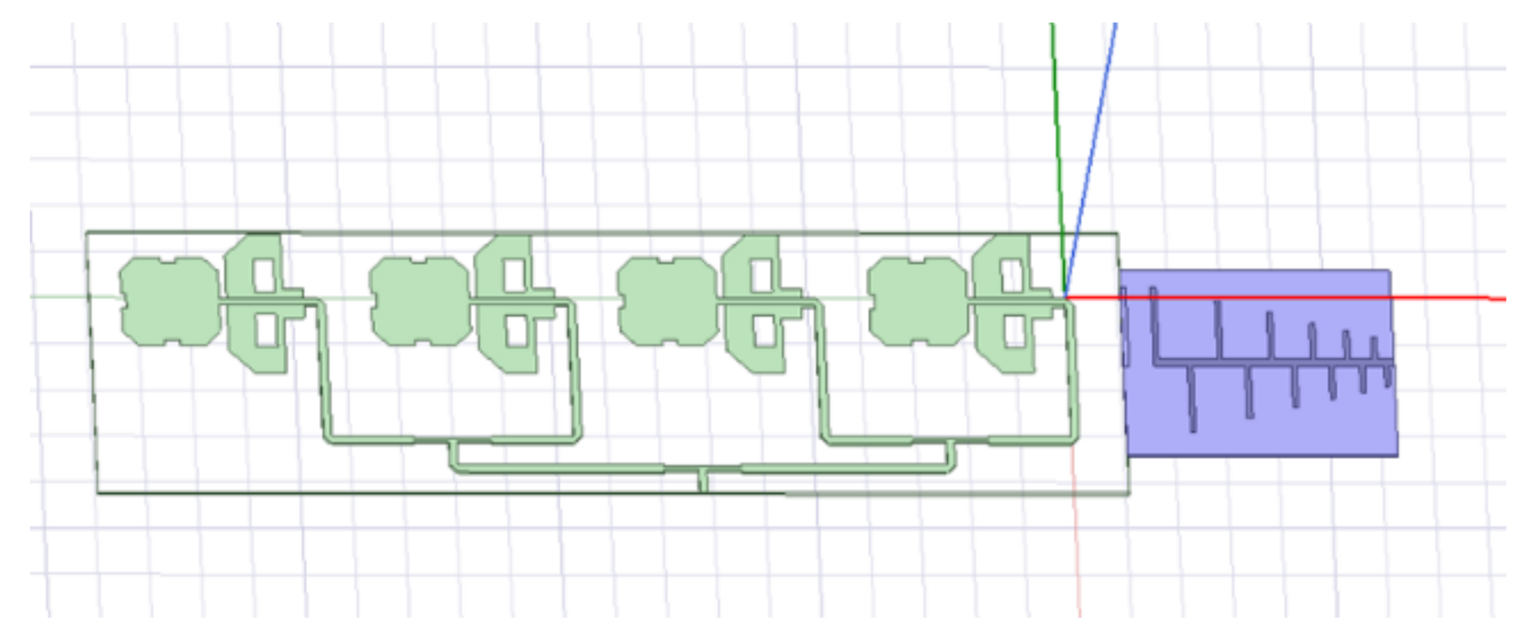
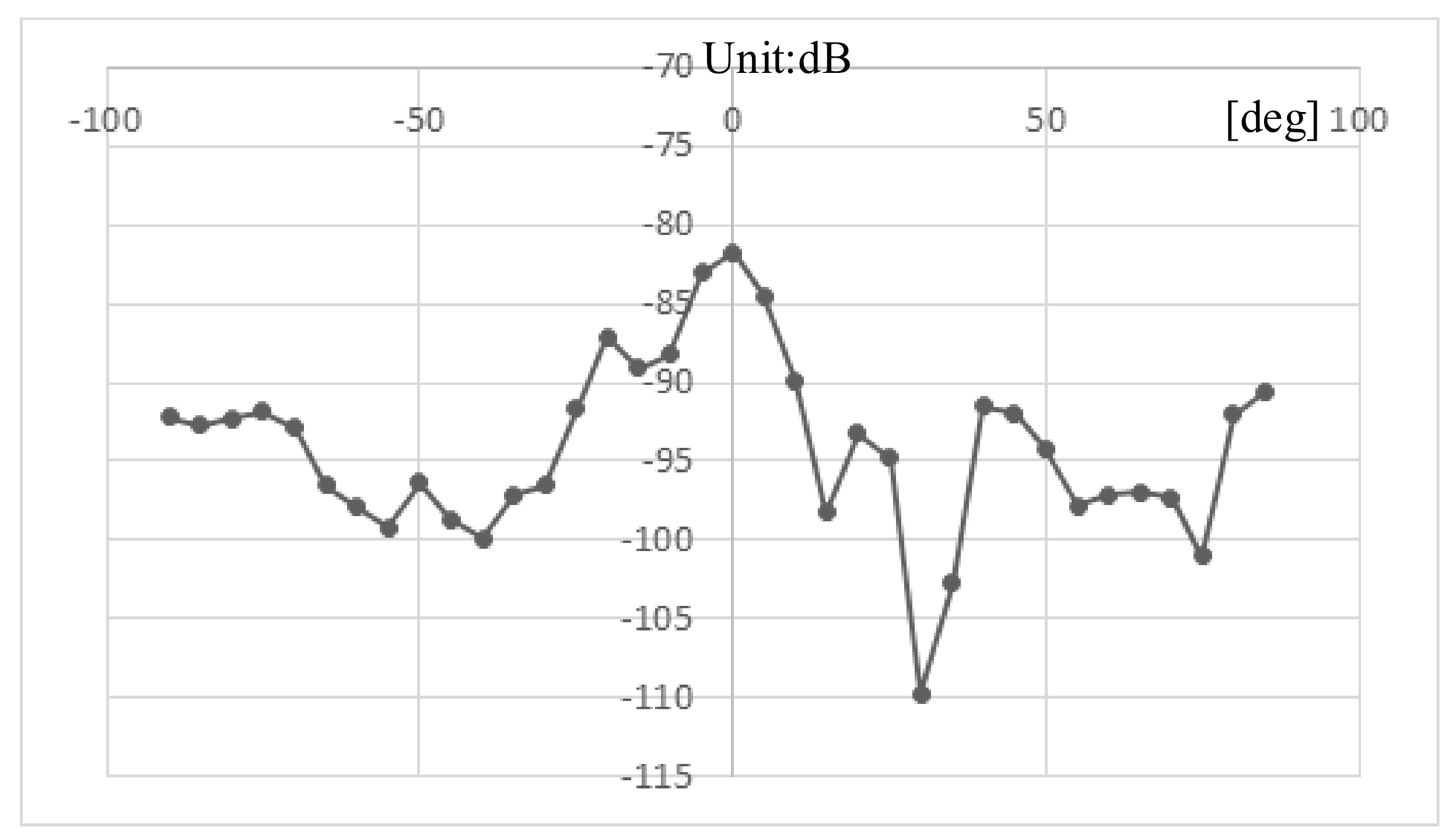
4. Simulation and Test Results

4.1. Simulation Results of the Two Antennas

Considering the relationship between the material properties of the dielectric substrate, the bandwidth, size and other properties of the antenna, and considering the radiation loss and surface wave of the antenna, the antenna is selected to be printed on a FR4 board with a thickness of 1.6 mm and a relative dielectric constant of 4.4, fed by the 50 Ω microstrip line, and the working frequency is 2~3.6 GHz. The design specifications of the antenna are shown in Table 4.
The pattern of the receiving antenna is shown in Figure 9. It can be seen that the E side is an omnidirectional antenna, and the H side is affected by the arrangement of the patch array, but it can be directed toward the upper and lower half spaces at the same time and radiation. The gain of the quad antenna array is 7.85 dB at 2.4 GHz. The feed network will increase some loss, but the impact on the antenna performance can be ignored, as shown in Figure 9a,b.
The improved transmitting antenna pattern and bandwidth are shown in Figure 10, Figure 11 and Figure 12. It can be seen from the figure that the improved transmitting antenna bandwidth is 1.76~3.96 GHz, that is, the bandwidth of 2.2 GHz. Compared with the 300 MHz bandwidth extension before the improvement, the gain is about 5.71 dB, and the directivity is basically unchanged.
The optimization result of transmitting antenna using a multi-objective genetic algorithm is shown in the figure below.
In Figure 13, a comparison of the directional patterns before and after optimization is shown. The antenna gain is optimized from 5.71 dB to 7 dB. Before optimization, there is a large side lobe, and the maximum side lobe level is −4 dB. After optimization, the maximum side lobe is reduced to −5.76 dB, which effectively enhances the directivity of the antenna.
The curves shown in Figure 14 and Figure 15 respectively show the change of return loss S11 and VSWR with respect to the frequency before and after optimization. It can be seen that the optimized 10 dB impedance bandwidth is 2.5 GHz, and the average VSWR in the frequency band is 1.3, reaching the expected goal.

4.2. Anechoic Chamber Test

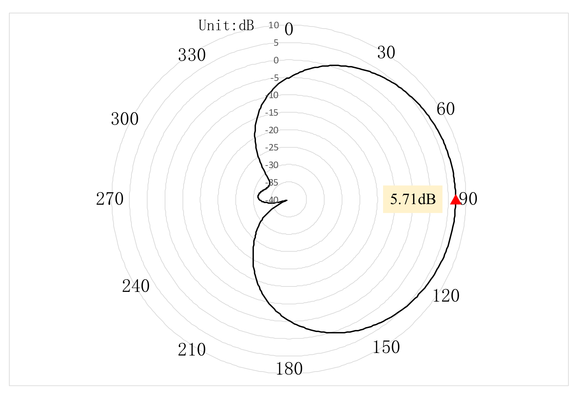
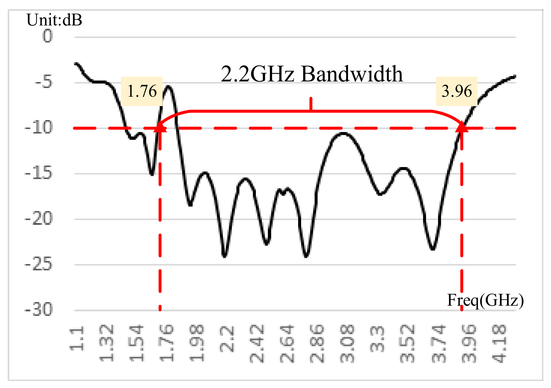
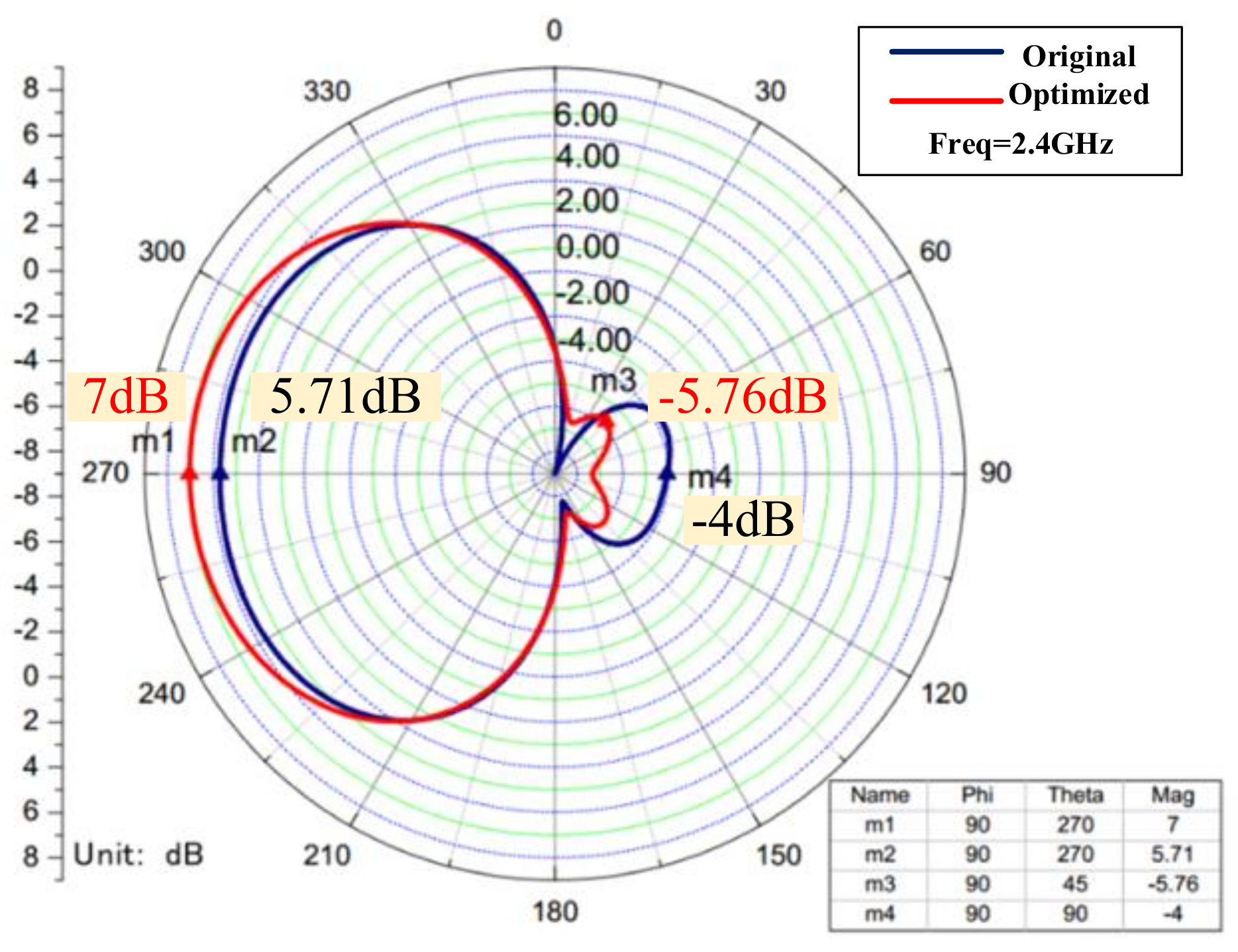
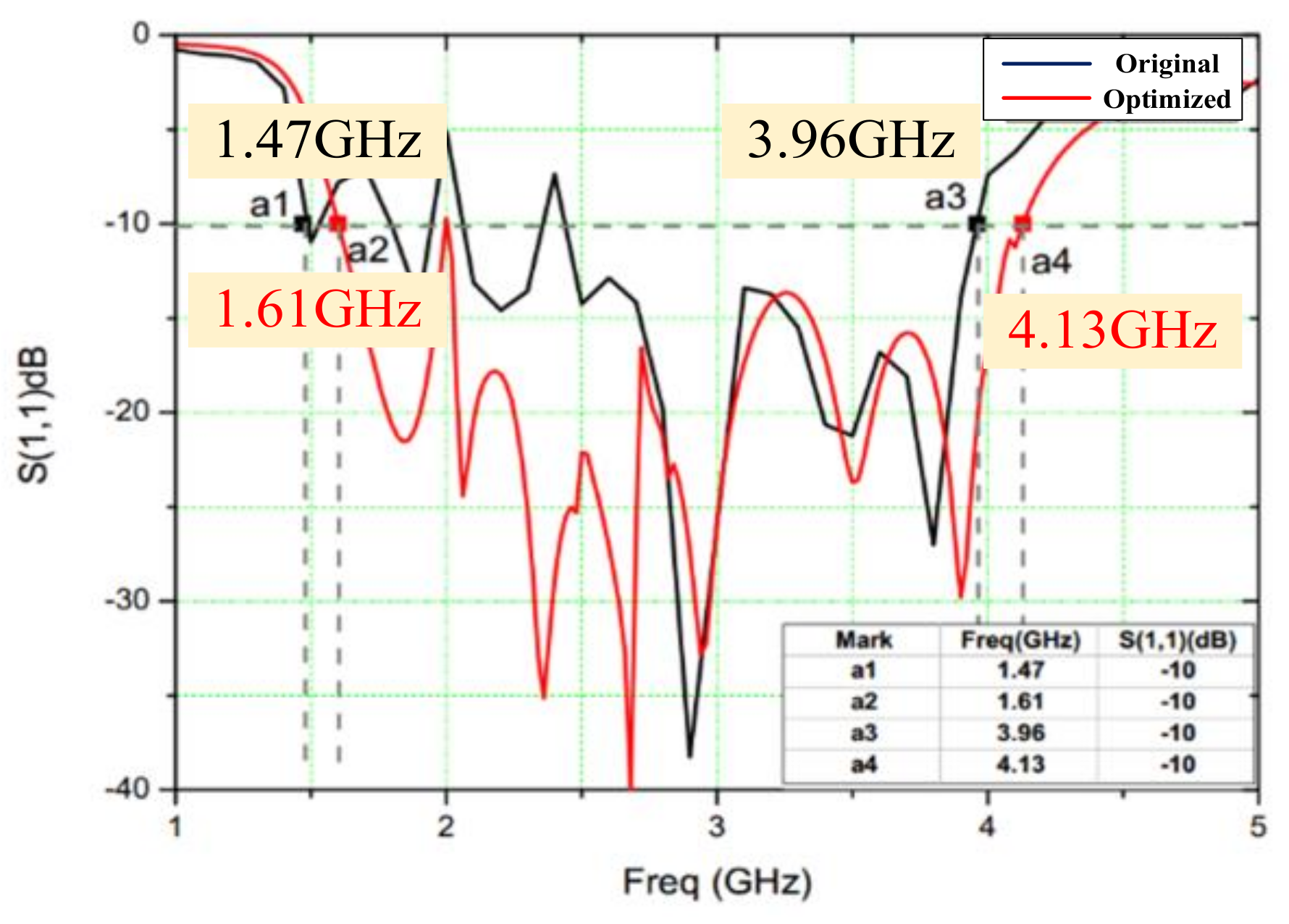
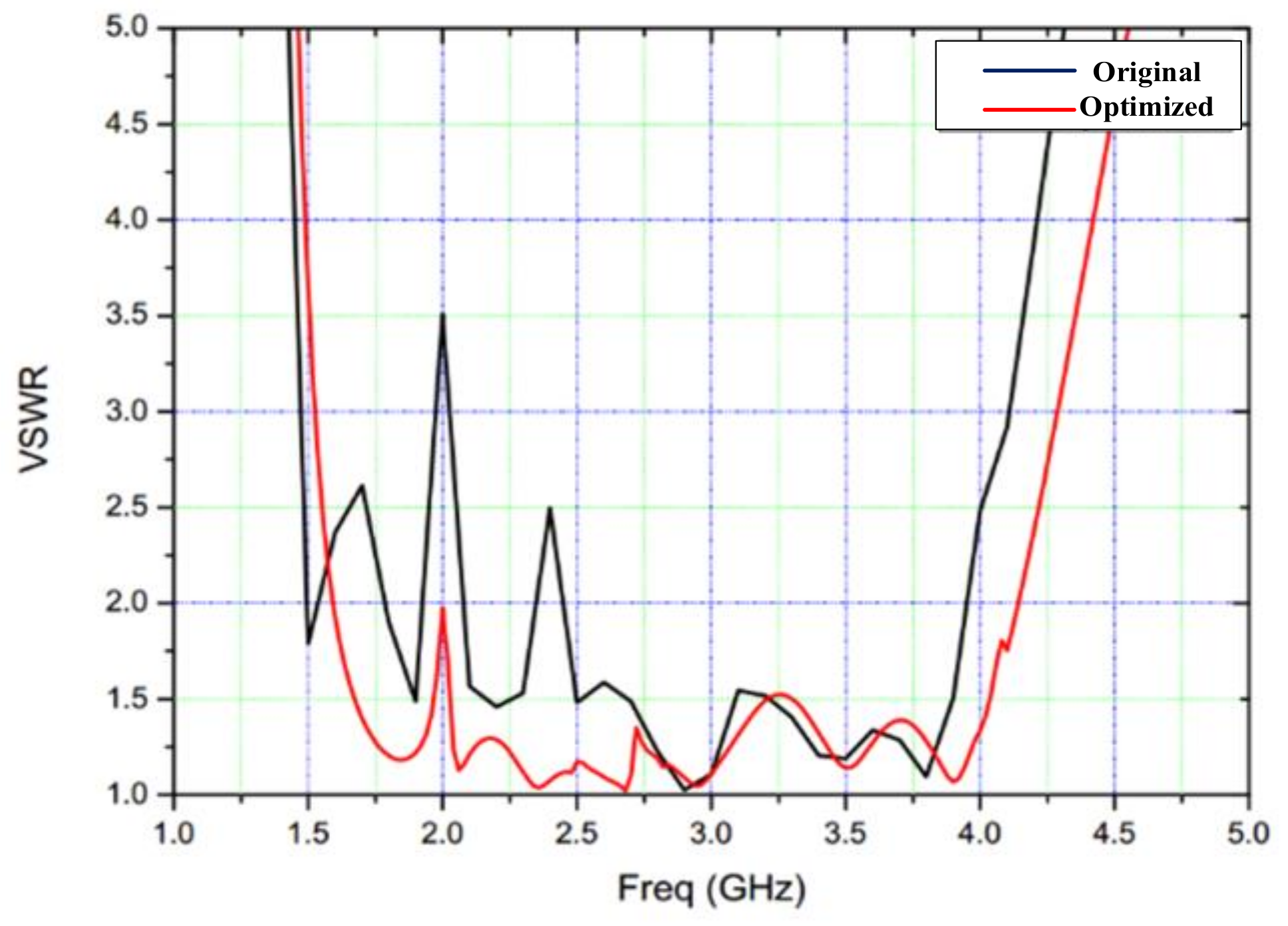
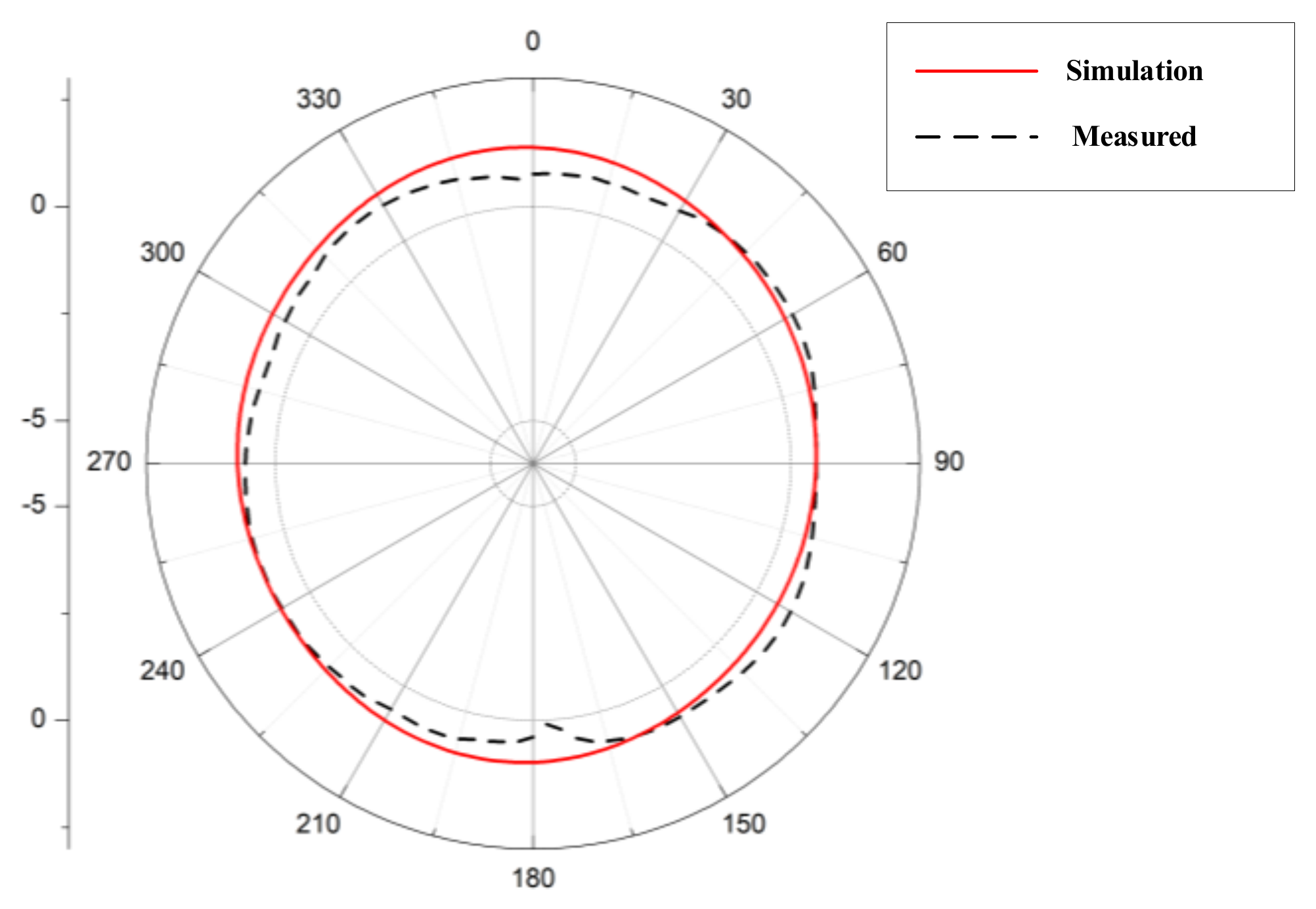
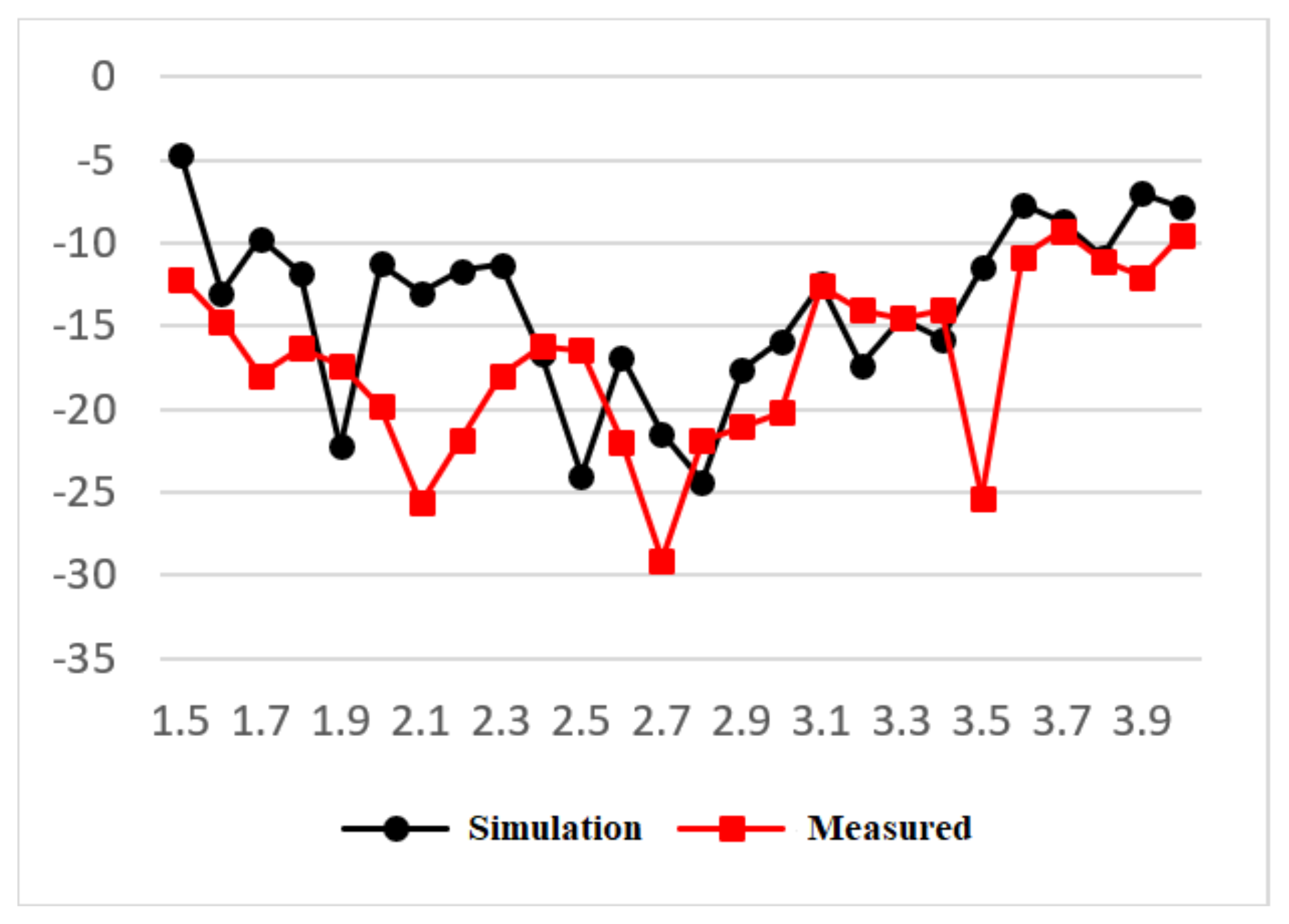
4.2.1. Receiving Antenna Performance Verification

The actual receiving antenna is shown in Figure 16. The pattern of the receiving antenna is shown in Figure 17. It can be seen that the actual measurement results of the patch antenna are consistent with the simulation results, and the pattern is omnidirectional. The recessed part of the antenna in the picture is related to the actual production of the antenna, and the wiring port causes interference within a certain range of the antenna pattern. This problem also exists in the measurement of other antennas, so it can be ignored.
The measured S11 curve of the antenna is shown in Figure 18. It can be seen that the antenna performance is good, which is similar to the simulation result, and the actual bandwidth is 1.5~3.8 GHz.

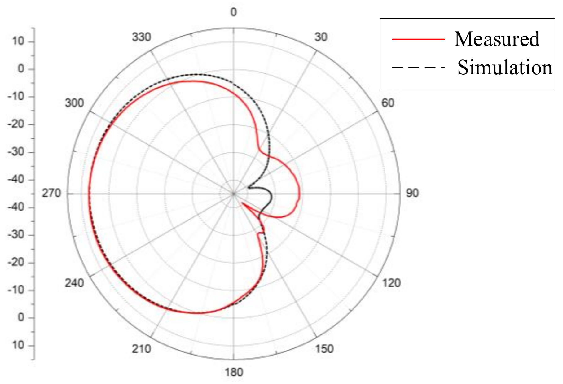
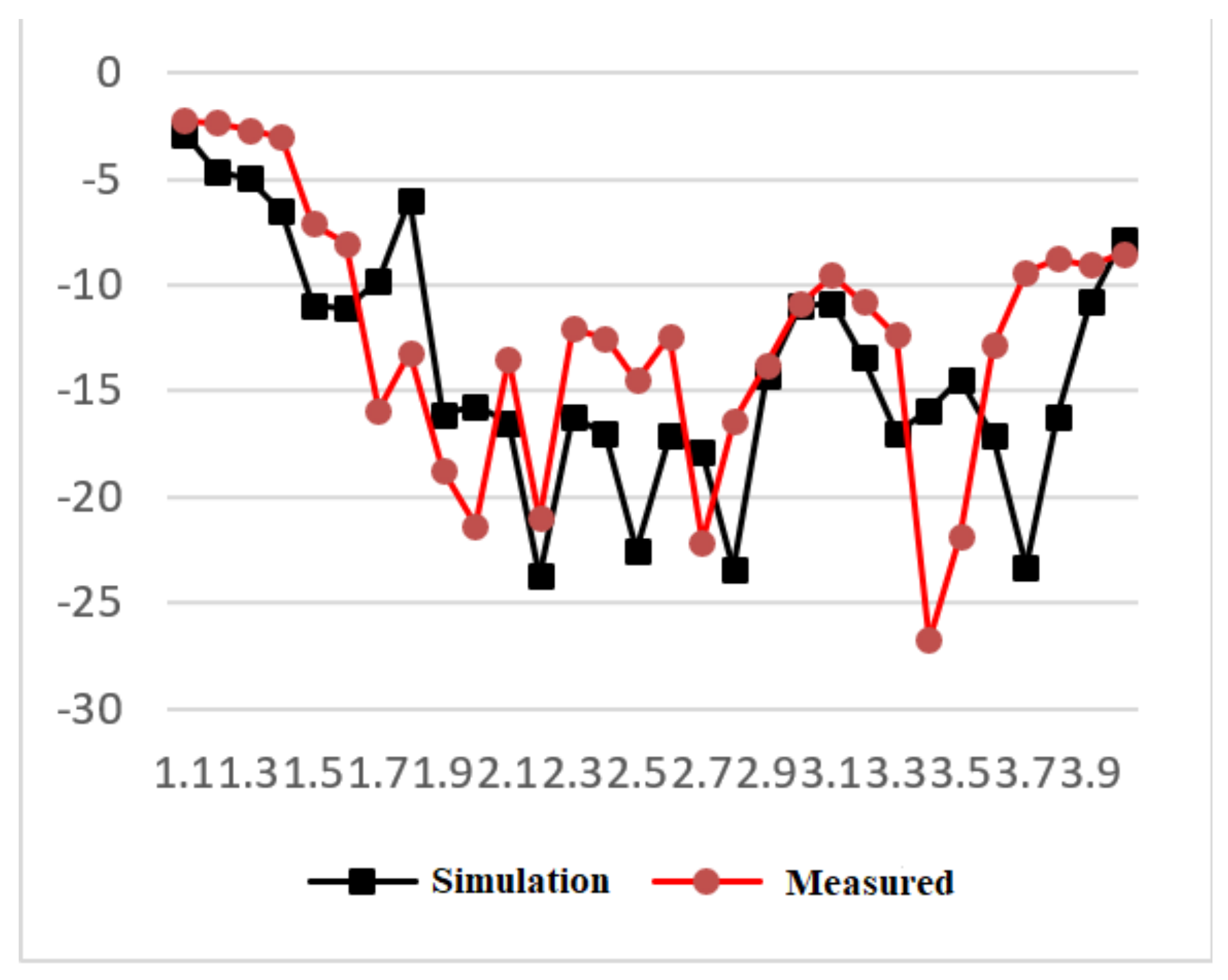
4.2.2. Transmitting Antenna Performance Verification

The measured result of the transmitting antenna pattern is shown in Figure 19. It can be seen that the actual measurement results of the log-period antenna are consistent with the simulation results. The properties of the antenna S11 are shown in Figure 20, and the physical bandwidth is 1.7~3.7 GHz.

4.2.3. Transceiver Module Performance Verification

According to the analysis result of the HFSS simulation software, the physical object of the complete environmental backscatter tag antenna is shown in Figure 21. The port of the four-element microstrip antenna is connected to the short array end of the log-period antenna through a coaxial line, and there is no external feed. The final transceiver module has a length of 505 mm, a width of 113.15 mm, and a thickness of 1.6 mm.
Since the dual antennas are passive, the following measurement scheme is adopted. The schematic diagram of the scheme is shown in Figure 22. Among them, S is a horn antenna, which is used to simulate the radio frequency signal source in the environment, and the transmission power is 20 dBm; PR represents the designed reflector antenna, which is placed on the turntable; BE represents the receiving end. When the turntable stops to 0°, the transmitting end of the PR is facing the BE, and the received power of the BE at this time is measured. When the turntable continues to rotate, make the BE deviate from the direction of the PR, and measure the received power of the BE again. Since the receiving antenna is an approximately omnidirectional antenna, the received power is assumed to be constant. By comparing the difference between the received power when the antenna is aligned and deviated from BE multiple times, the directivity of the antenna channel model can be reflected. The measurement system is shown in Figure 23.
The power received by BE is shown in Figure 24. Turn the turntable from −90° to +90°. When the angle is 0°, the received power is the maximum, which is −82 dB. When the receiving end deviates from the main channel direction by 30°, the received power decreases to −110 dB. It can be seen from the curve that when the receiving end deviates from the main channel direction, the received power of BE will decrease rapidly, that is, the power received by the receiving end will decrease.
The non-line-of-sight propagation path from the transmitting antenna to the receiving antenna mainly includes a reflection path, a diffraction path, and a scattering path. These three paths have high losses. When the passive repeater exists, an independent re-radiation path is added, so the signal quality of the non-line-of-sight channel can be improved, and the signal coverage of the blind zone can be enhanced.

5. Conclusions

The environmental backscatter technology is gradually popularized and used because it gets rid of the energy coverage limitation of the reader in the communication of the Internet of Things. Based on the ubiquitous power Internet of Things and 5G technology, this article discusses the important role of backscatter communication technology in the smart grid, and aims at the short communication distance, unstable energy and low reliability of existing tag antennas. From the perspective of the physical layer, design a tag antenna with a dual-antenna structure, taking into account its own energy supply and signal forwarding functions, and using a multi-objective genetic algorithm to optimize the antenna size. Later simulation and actual measurement results show that the antenna gain is obvious, the side lobe is small, the bandwidth is as expected, and the anti-interference is strong. It solves the low reliability of the traditional microwave electronic tag antenna in the power Internet of Things environment. Problems such as instability and short transmission distance meet the information transmission requirements in the power Internet of Things scenario.
In view of the optimization results that have been achieved, future design work has the following improvement ideas: According to the analysis of the actual measurement results, the receiving power of the receiving antenna can still be increased, so the receiving antenna can be further improved; the beam width of the transmitting antenna is still not narrow enough, and a design can be designed. A planar antenna that takes into account both bandwidth and directivity; the receiving antenna and the transmitting antenna can be separated from each other to prevent interference from the antenna pattern, which can reduce the size of the antenna integration.

Author Contributions

Conceptualization, J.Z.; methodology, T.H.; software, X.C.; validation, T.H.; formal analysis, X.C. and P.W.; investigation, X.C. and T.H.; resources, T.H.; data curation, X.C.; writing—original draft preparation, X.C.; writing—review and editing, X.C. and S.Z.; visualization, X.C.; supervision, T.H.; project administration, T.H. All authors have read and agreed to the published version of the manuscript.

Funding

The work by Tao Hong is supported by National Natural Science Foundation of China under grant number 61827901.

Conflicts of Interest

The authors declare no conflict of interest.

References

  1. Song, S.M.; Yao, W.J. Research on the Application Value of Wireless Mesh Network in Power Equipment of the UPIOT. J. Phys. Conf. Ser. 2019, 1346, 012046. [Google Scholar] [CrossRef] [Green Version]
  2. Wang, Q.; Zhao, D.; Yang, B.; Li, C. Risk assessment of the UPIoT construction in China using combined dynamic weighting method under IFGDM environment. Sustain. Cities Soc. 2020, 60, 102199. [Google Scholar] [CrossRef]
  3. Kang, C.H.; Lee, W.S.; You, Y.H.; Song, H.K. Signal detection scheme in ambient backscatter system with multiple antennas. IEEE Access 2017, 5, 14543–14547. [Google Scholar] [CrossRef]
  4. Gope, P.; Amin, R.; Islam, S.H.; Kumar, N.; Bhalla, V.K. Lightweight and privacy-preserving RFID authentication scheme for distributed IoT infrastructure with secure localization services for smart city environment. Future Gener. Comput. Syst. 2018, 83, 629–637. [Google Scholar] [CrossRef]
  5. Darsena, D. Noncoherent detection for ambient backscatter communications over OFDM signals. IEEE Access 2019, 7, 159415–159425. [Google Scholar] [CrossRef]
  6. Parks, A.N.; Liu, A.; Gollakota, S.; Smith, J.R. Turbocharging ambient backscatter communication. ACM SIGCOMM Comput. Commun. Rev. 2014, 44, 619–630. [Google Scholar] [CrossRef]
  7. Bharadia, D.; Joshi, K.R.; Kotaru, M.; Katti, S. Backfi: High throughput wifi backscatter. ACM SIGCOMM Comput. Commun. Rev. 2015, 45, 283–296. [Google Scholar] [CrossRef]
  8. El Mossallamy, M.; Han, Z.; Pan, M.; Jantti, R.; Seddik, K.; Li, G.Y. Noncoherent frequency shift keying for ambient backscatter over OFDM signals. In Proceedings of the ICC 2019–2019 IEEE International Conference on Communications (ICC), Shanghai, China, 20–24 May 2019; pp. 1–6. [Google Scholar]
  9. Xu, C.; Yang, L.; Zhang, P. Practical backscatter communication systems for battery-free Internet of Things: A tutorial and survey of recent research. IEEE Signal Process. Mag. 2018, 35, 16–27. [Google Scholar] [CrossRef]
  10. Guo, J.; Durrani, S.; Zhou, X. Monostatic backscatter system with multi-tag to reader communication. IEEE Trans. Veh. Technol. 2019, 68, 10320–10324. [Google Scholar] [CrossRef]
  11. Pereira, F.; Sampaio, H.; Chaves, R.; Correia, R.; Luís, M.; Sargento, S.; Jordão, M.; Almeida, L.; Senna, C.; Oliveira, A.S.R.; et al. When backscatter communication meets vehicular networks: Boosting crosswalk awareness. IEEE Access 2020, 8, 34507–34521. [Google Scholar] [CrossRef]
  12. Chen, C.; Wang, G.; Guan, H.; Liang, Y.C.; Tellambura, C. Transceiver design and signal detection in backscatter communication systems with multiple-antenna tags. IEEE Trans. Wirel. Commun. 2020, 19, 3273–3288. [Google Scholar] [CrossRef]
  13. Amato, F.; Occhiuzzi, C.; Marrocco, G. Epidermal backscattering antennas in the 5G framework: Performance and perspectives. IEEE J. Radio Freq. Identif. 2020, 4, 176–185. [Google Scholar] [CrossRef]
  14. Zhang, J.; Lv, L.; Zhu, M.; Zhang, Q. Research on Intelligent Substation Wireless Sensor Network System Architecture Based on Internet of Things Technology. In Proceedings of the 2020 Prognostics and Health Management Conference (PHM-Besançon), Besancon, France, 4–7 May 2020; pp. 324–327. [Google Scholar]
  15. Hussien, N.; Ajlan, I.; Firdhous, M.M.; Alrikabi, H. Smart Shopping System with RFID Technology Based on Internet of Things. iJIM 2020, 14, 17–29. [Google Scholar] [CrossRef]
  16. Min, X.; Kuang, W. Study on the ecological farming control system based on the Internet of Things. Wirel. Pers. Commun. 2018, 102, 2955–2967. [Google Scholar] [CrossRef]
  17. Sharif, A.; Li, J.P.; Saleem, M.A. Internet of things enabled vehicular and ad hoc networks for smart city traffic monitoring and controlling: A review. Int. J. Adv. Netw. Appl. 2018, 10, 3833–3842. [Google Scholar] [CrossRef]
  18. Chen, Q. Research on Implementation Strategy of Ubiquitous Power Internet of Things. Power Gener. Technol. 2019, 40, 99. [Google Scholar]
  19. Liu, Y.; Yang, C.; Jiang, L.; Xie, S.; Zhang, Y. Intelligent edge computing for IoT-based energy management in smart cities. IEEE Netw. 2019, 33, 111–117. [Google Scholar] [CrossRef]
  20. Liang, X.; Sun, D.; Li, W. Composition Form and Function Configuration of Intelligent Terminal Based on Edge Computing for Power Internet of Things. IOP Conf. Ser. Earth Environ. Sci. 2021, 621, 012058. [Google Scholar] [CrossRef]
  21. Amato, F.; Torun, H.M.; Durgin, G.D. RFID backscattering in long-range scenarios. IEEE Trans. Wirel. Commun. 2018, 17, 2718–2725. [Google Scholar] [CrossRef]
  22. Zhang, J.; Tian, G.Y.; Marindra, A.M.; Sunny, A.I.; Zhao, A.B. A review of passive RFID tag antenna-based sensors and systems for structural health monitoring applications. Sensors 2017, 17, 265. [Google Scholar] [CrossRef]
  23. Pawłowicz, B.; Salach, M.; Trybus, B. Smart city traffic monitoring system based on 5G cellular network, RFID and machine learning. In KKIO Software Engineering Conference; Springer: Cham, Switzerland, 2018; pp. 151–165. [Google Scholar]
  24. Khan, S.F. Health care monitoring system in Internet of Things (IoT) by using RFID. In Proceedings of the 2017 6th International Conference on Industrial Technology and Management (ICITM), Cambridge, UK, 7–10 March 2017; pp. 198–204. [Google Scholar]
  25. Casula, G.A.; Maxia, P.; Mazzarella, G.; Montisci, G. Design of a printed log-periodic dipole array for ultra-wideband applications. Prog. Electromagn. Res. 2013, 38, 15–26. [Google Scholar] [CrossRef] [Green Version]
  26. Shen, X.; Liu, Y.; Zhao, L.; Huang, G.L.; Shi, X.; Huang, Q. A miniaturized microstrip antenna array at 5G millimeter-wave band. IEEE Antennas Wirel. Propag. Lett. 2019, 18, 1671–1675. [Google Scholar] [CrossRef]
  27. Xu, Z.M.; Wu, Y.W.; Tao, M.C.; Hao, Z.C. A Frequency Reconfigurable Slot Antenna Backed by the Substrate Integrated Waveguide Cavity for 5G Applications. In Proceedings of the 2019 International Conference on Microwave and Millimeter Wave Technology (ICMMT), Guangzhou, China, 19–22 May 2019; pp. 1–3. [Google Scholar]
  28. Sun, Y.; Liu, Y.; Tang, N.; Xu, D.; Li, Y.; Yu, Y.; Zhang, K.; Gou, Q.; Du, Z. The design of end-fire antenna with log-period directors. In Proceedings of the 2018 International Workshop on Antenna Technology (iWAT), Nanjing, China, 5–7 March 2018; pp. 1–3. [Google Scholar]
  29. McLean, J. Topology for Maintaining Symmetry in Hybrid LPDA-Broadband-Dipole Antennas. In Proceedings of the 2019 Antenna Measurement Techniques Association Symposium (AMTA), San Diego, CA, USA, 6–11 October 2019; pp. 1–6. [Google Scholar]
  30. Chang, L.; He, S.; Zhang, J.Q.; Li, D. A compact dielectric-loaded log-periodic dipole array (LPDA) antenna. IEEE Antennas Wirel. Propag. Lett. 2017, 16, 2759–2762. [Google Scholar] [CrossRef]
  31. Shi, Y.; Meng, Z.K.; Wei, W.Y.; Zheng, W.; Li, L. Characteristic mode cancellation method and its application for antenna RCS reduction. IEEE Antennas Wirel. Propag. Lett. 2019, 18, 1784–1788. [Google Scholar] [CrossRef]
  32. Mirjalili, S. Genetic algorithm. In Evolutionary Algorithms and Neural Networks; Springer: Cham, Switzerland, 2019; pp. 43–55. [Google Scholar]
  33. Smith, J.S.; Baginski, M.E. Thin-wire antenna design using a novel branching scheme and genetic algorithm optimization. IEEE Trans. Antennas Propag. 2019, 67, 2934–2941. [Google Scholar] [CrossRef]
Figure 1. Smart grid network architecture.
Electronics 10 01521 g001
Figure 2. Using dual antenna system to solve the signal coverage of blind area in complex terrain.
Electronics 10 01521 g002
Figure 3. Microstrip antenna array model.
Electronics 10 01521 g003
Figure 4. Broadband microstrip antenna unit model.
Electronics 10 01521 g004
Figure 5. Broadband microstrip antenna array model.
Electronics 10 01521 g005
Figure 6. Log-period antenna with parasitic patch.
Electronics 10 01521 g006
Figure 7. Transceiver antenna model.
Electronics 10 01521 g007
Figure 8. Multi-objective genetic algorithm graph.
Electronics 10 01521 g008
Figure 9. Improved four-element patch antenna pattern.
Electronics 10 01521 g009
Figure 10. Improved transmitting antenna pattern.
Electronics 10 01521 g010
Figure 11. Improved transmitting antenna S11.
Electronics 10 01521 g011
Figure 12. Improved transmitting antenna VSWR.
Electronics 10 01521 g012
Figure 13. Comparison of transmitting antenna patterns before and after optimization.
Electronics 10 01521 g013
Figure 14. Transmitting antenna S11 before and after optimization.
Electronics 10 01521 g014
Figure 15. Transmitting antenna VSWR before and after optimization.
Electronics 10 01521 g015
Figure 16. Receiving antenna in kind.
Electronics 10 01521 g016
Figure 17. Measured and simulated pattern of receiving antenna.
Electronics 10 01521 g017
Figure 18. Receiving antenna simulation and measured S11 curve.
Electronics 10 01521 g018
Figure 19. Transmitting antenna measured and simulated pattern.
Electronics 10 01521 g019
Figure 20. Transmitting antenna simulation and measured S11 curve.
Electronics 10 01521 g020
Figure 21. Transceiver module in kind.
Electronics 10 01521 g021
Figure 22. The physical object of the environmental backscatter tag antenna.
Electronics 10 01521 g022
Figure 23. Measurement system display.
Electronics 10 01521 g023
Figure 24. BE horn receiving power change with angle.
Electronics 10 01521 g024
Table 1. Size of patch antenna with improved structure (mm).
gt1t2w1h1Lw2
389.66627114
h2w3h3widw4h4
823.68357.230
Table 2. Original size of log-periodic antenna (mm).
L1L2L3L4L5L6L7
3632.42926.123.521.319.2
L8L9L10L11L12d1d2
17.115.51412. 511.21312
d3d4d5d6d7d8d9
10.59.58.67.77.06.15.5
d10d11LW
5.14.51302
Table 3. Optimized log-period antenna size (mm).
L1L2L3L4L5L6L7
3632.429.1626.2423.6221.2619.2
L8L9L10L11L12d1d2
17.2215.5013.9512.5511.301311.7
d3d4d5d6d7d8d9
10.539.488.537.686.916.225.60
d10d11LW
5.044.531302
Table 4. Antenna design indicators.
ParameterValue
Working frequency2 GHz~3.6 GHz
Receiving antenna gain>6.5 dB
Transmitting antenna gain>6.5 dB
Maximum VSWR in bandwidth<2
Average VSWR<1.3
Maximum side lobe level<−4 dB
Return loss<−10 dB
Antenna size<50 cm
Publisher’s Note: MDPI stays neutral with regard to jurisdictional claims in published maps and institutional affiliations.

