Review

Categorization and SEU Fault Simulations of Radiation-Hardened-by-Design Flip-Flops

Department of Electrical and Computer Engineering, University of Pittsburgh, Pittsburgh, PA 15261, USA
*
Author to whom correspondence should be addressed.
Electronics 2021, 10(13), 1572; https://doi.org/10.3390/electronics10131572
Submission received: 25 May 2021 / Revised: 18 June 2021 / Accepted: 25 June 2021 / Published: 30 June 2021

Abstract

:
In the previous three decades, many Radiation-Hardened-by-Design (RHBD) Flip-Flops (FFs) have been designed and improved to be immune to Single Event Upsets (SEUs). Their specifications are enhanced regarding soft error tolerance, area overhead, power consumption, and delay. In this review, previously presented RHBD FFs are classified into three categories with an overview of each category. Six well-known RHBD FFs architectures are simulated using a 180 nm CMOS process to show a fair comparison between them while the conventional Transmission Gate Flip-Flop (TGFF) is used as a reference design for this comparison. The results of the comparison are analyzed to give some important highlights about each design.

1. Introduction

When an energetic particle hits a logic circuit, it can introduce a temporary voltage disturbance due to charge depositing that can upset sensitive circuit nodes and propagate to the successive blocks [1]. Electron-hole pairs are generated corresponding to the strike of an ionizing particle with the transistor nodes, resulting in a generated charge that depends on the Linear Energy Transfer (LET) of the striking particle. At a certain threshold, this charge becomes critical and causes a soft error that flips the logic output [2]. These events are known as Single Event Transients (SETs), and they can be latched by registers causing an error in the stored bits, which is called Single Event Upsets (SEUs) [1,2]. Mitigating SEU is crucial in space and nuclear applications due to the existence of higher energetic particles such as heavy ions and protons [1,3]. Recently, SEU has become a terrestrial problem in modern nanoscale CMOS technology since a small amount of charge can upset the data stored in the Flip-Flops (FFs) [4].
Two techniques can be implemented in the device level of the FF to increase its immunity to SEU that are Radiation-Hardened-by-Process (RHBP) and Radiation-Hardened-by-Design (RHBD) [5]. The first technique is executed at the fabrication process of the CMOS transistors by modifying their geometrical parameters. The other technique concerns the FF architecture such as redundancy and filtering. It is independent of the technology size but results in some overhead in area, power, delay, or cost.
RHBD FFs, in this review, are classified into three different categories; they are spatial redundancy FF that makes different copies of the same FF in space [1,6,7,8,9], temporal redundancy FF that compares the signal at different times by adding some delay [10,11,12,13,14], and node hardening FF that strengthens the internal nodes of the FFs and protects them from flipping by soft errors [4,15,16,17,18,19,20,21,22]. Additionally, some FFs can be categorized into multiple categories such as spatial–temporal redundancy FF [7,23,24,25,26] or node hardening FF with spatial/temporal redundancy [27,28].
This review focuses on RHBD FFs. First, it introduces the Conventional Transmission Gate FF (TGFF) in Section 2, showing its structure and how it is affected by soft errors. Section 3 classifies the different topologies of RHBD FFs into three main categories. Section 4 presents the simulation results of some selected well-known RHBD FFs regarding their radiation resilience using a 180 nm CMOS process. Finally, Section 5 concludes this review.

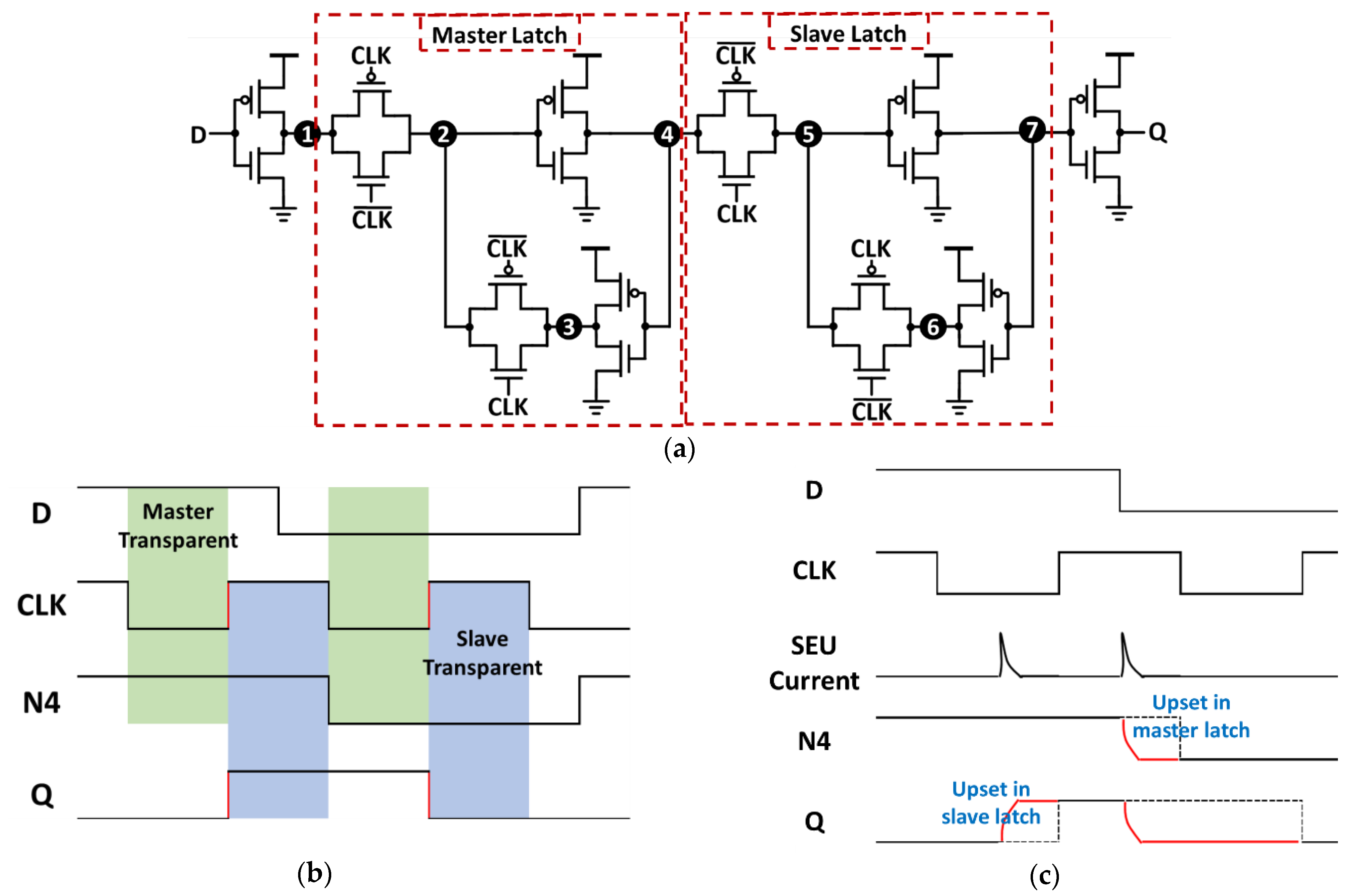
2. Conventional Transmission Gate Flip-Flop (TGFF)

Conventional TGFF is a well-known FF topology that is used in many earlier microprocessors and it is a modified version of the popular FF used in the PowerPC 603 processor (NXP Semiconductors, Eindhoven, Netherlands) [29,30,31]. Figure 1a shows the circuit diagram of TGFF, which consists of a master latch that captures the input D signal when the CLK is low and keeps it when the CLK is high; and a slave latch that operates on the opposite CLK levels as the signal is passed from master latch to slave latch while the CLK is high, and it is kept as long as the CLK is low. Accordingly, the signal has to pass through the master latch during the CLK = 0 and pass through the slave latch during the CLK = 1, which means that the input signal D is only transferred to the output Q when the CLK changes from 0 to 1 (Positive edge of the CLK) as illustrated in Figure 1b.
Conventional TGFF has a relatively small area and is one of the most power-efficient topologies compared to other master–slave latch-pairs [31], which makes it a good candidate to be used as a benchmark to compare other FFs. However, TGFF is weaker against soft errors by order of ~2× or ~3× than other RHBD FF [32]. The master latch of TGFF can be easily upset by the soft errors that happen when the CLK is high (in the hold state of the master latch) while the slave latch can be upset when the CLK is low (in the hold state of the slave latch) as shown in Figure 1c. Additionally, soft errors can affect TGFF during the transparent state if this error is propagated and latched by the next latch [6].

3. Radiation-Hardened-by-Design Flip-Flops (RHBD FF)

There are numerous designs for RHBD FF. In this review, we divide them into three main categories, which are spatial redundancy, temporal redundancy, and nodes hardened.

3.1. Spatial Redundancy FF

SEU is collected by a single node at a certain time. Spatial redundancy FF designs make replicas of each logic and check their outputs to detect the error or correct it [6]. XOR gate can be used to compare the output of two redundant FFs and produces an error signal if they do not match. To determine the correct output, a third FF is required, and a majority voter circuit is connected to the output of the three FFs. This design is considered one of the most popular RHBD FFs, which is well-known as Triple Modular Redundancy (TMR) FF, and it is illustrated in Figure 2a [1,7]. TMR FF is very immune to soft errors, but it requires a 3× larger area than the conventional TGFF, and thus exhibiting 3× power consumption overhead.
TMR stills can fail to SEU in advanced nanoscale technologies due to charge sharing accompanied by the decreased distance between transistors [6]. However, the charge sharing effect can be reduced by proper layout techniques.
The majority voter circuit, shown in Figure 2b, simply consists of two-level NAND gates that generate an output that agrees with any two consistent inputs. If only one FF is upset, the majority voter ignores it and keeps the correct output relying on the other two correct FFs as demonstrated in Figure 2c. Since the voter is connected to the output of the three replicas, if the particle hits the voter circuit with enough charge, it can flip the final output [6]. However, this fault is instantaneous and it is not latched.

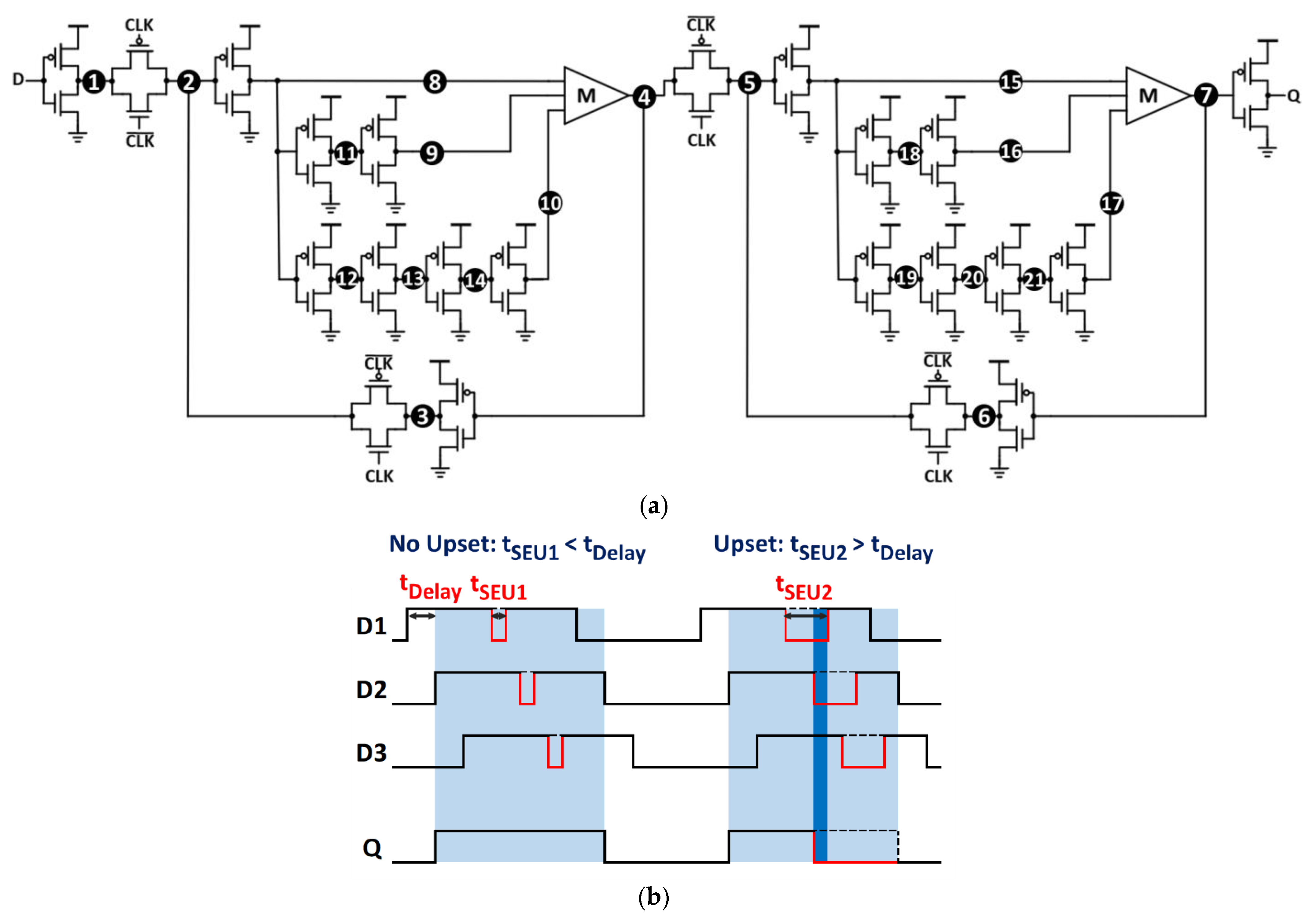
3.2. Temporal Redundancy FF

Another technique that can help in countering soft errors is to make delayed replicas at different times of the same signal and vote between them as shown in Figure 3a. This makes the FF resists the SEU effect as long as the delay time is larger than the SEU current period. Figure 3b. shows how the delay time can affect the resilience of the FF to the soft error [10]. On the left side of the figure, the soft error time is less than the delay time which makes the disturbance takes effect at a different time, and at any certain moment, the majority voter circuit sees at least two correct inputs. Accordingly, the FF can tolerate the error by voting between three signals easily. On the other hand, if the soft error time exceeds the delay time, two signals would suffer from disturbance at the same time resulting in a fault at the final output. One major disadvantage of the added delay elements is reducing the maximum allowable frequency that the temporal redundancy FF can operate at. This is because the signal path with the longest delay elements would significantly increase the CLK to Q delay of the FF, which makes it unsuitable for high-speed applications.

3.3. Node Hardened FF

This category comprises any design technique that relies on protecting or hardening the internal nodes of the FF and makes them difficult to flip by soft errors. Dual Interlocked storage Cell (DICE) FF, shown in Figure 4, is one of the most common techniques in this category.
The logic states of any node in the DICE latch are controlled by two adjacent nodes, so the DICE latch requires two simultaneous nodes with the same logic to be flipped to change its state, while the soft error that hits only one node at a time will be tolerated [15]. DICE is classified here as a node hardened FF; however, it can also be classified as a spatial redundancy FF [4]. There is another node hardened latch that has four storage nodes as a DICE latch, Quatro latch [17].
Node hardening can also be obtained by using stacked inverters instead of standard inverters as it is stronger to soft errors [18]. This method is immune to soft errors when it is used with Silicon on Thin Box (SOTB) process, which prevents the charge sharing effect because a BOX layer isolates transistor channels. Accordingly, the output of the stacked inverters flips only when both of its nMOS transistors are hit by energetic particles at the same time [19]. One drawback of this method is the increased delay because of the duplicated gate capacitance and output resistance compared to conventional FF. In [19,20] other FF designs using stacked transistors are implemented based on the adaptive coupling to reduce the power consumption and delay. A comparison between a stacked transmission-gate FF and a stacked tristate-inverter FF is presented in [22] shows a similar strength to soft errors of both FFs, while stacked tristate-inverter FF has less delay by 21% with a larger area by 9% than the stacked transmission-gate FF.
The fourth structure for node hardening [21] uses an RC filtering structure with an adaptive SEU detecting circuit to control the functions of the switches that automatically control the involved RC filtering structure in the sensitive nodes. This adaptivity makes the system able to select between higher speed or higher SEU immunity based on the detected values of the critical nodes.

3.4. Hybrid Hardened FF

The above three topologies can be combined to construct a hybrid topology. Figure 5a shows a combination of spatial–temporal redundancy FF that consists of TMR FF with delay elements [7]. This temporal-TMR FF can possess a higher soft error immunity even with the charge sharing effect. On the other hand, it suffers from the same size problem of the TMR FF and the speed problem of temporal redundancy FF. Another spatial–temporal redundancy FF is known as Dual Modular Redundancy (DMR) FF, shown in Figure 5b. It depends on two replicas of the conventional FF instead of three replicas as TMR [23]. The outputs of the two copies are connected to a C-element. The truth table of the C-element is shown in Table 1. The C-element delays the change in the final output until both copies of the FF agree together. Accordingly, even if one copy is upset, the final output keeps its previous state. A third spatial–temporal redundancy FF, radiation-hardened scan FF (RH-SFF) [24], corrects soft errors in the sequential element and its preceding combinational logic.
One more hybrid topology is shown in Figure 5c, which consists of a temporal master latch and a DICE slave latch [27]. Similar to temporal-TMR FF, the temporal-DICE FF can get the hardening advantages of both DICE and temporal redundancy, but it also suffers from the disadvantages of speed limitations due to delay elements.

4. Results and Measurements

This section shows the simulation results of previously presented seven FF topologies using a 180 nm process to compare their performance and soft error resilience. The use of a large process results in better radiation hardening because of the larger capacitance accompanied by their transistors, which requires a large amount of charge to upset it. This also can help us to compare different topologies without taking into consideration the charge sharing effect that can depend on different layouts. The simulated FFs are TGFF, TMR FF, temporal FF, DICE FF, temporal-TMR FF, DMR FF, and temporal-DICE FF.

4.1. The SEU Testbench

To judge the radiation resilience of the selected FFs, a double-exponential current source in (1) is generated using Verilog-A code to emulate the SEU effect [33]. It is injected at every node in each FF. The tested nodes are shown by numbered circles in Figure 1, Figure 2, Figure 3, Figure 4 and Figure 5.
I S E U = Q c o l l τ α τ β ( e t τ α e t τ β )
here, Q c o l l is the charge deposited upon the strike of the particle, τ α and τ β are the collection and falling time constants, and they are selected to be 200 ps and 50 ps respectively [34,35]. Figure 6a shows the SEU current testbench that is created to test the selected FF while injecting the SEU current at the following cases:
  • Both positive and negative SEU spikes are tested, by changing both Sp and Sn switches simultaneously in Figure 6a.
  • SEU current is injected at the two cases of input D; high input (D = 1) and low input (D = 0) as shown in Figure 6b.
  • For each input case, SEU current is timed at the positive edge of the clock and when the clock level is stable as shown in Figure 6b by the yellow thunder symbols.
  • A wide range of clock frequencies is applied (100 MHz, 250 MHz, 500 MHz, 1 GHz, 2 GHz).
  • An extended range of the deposited charge (Qcoll) is used (1 fC to 2.16 pC).
Qcoll of 2.16 pC is equivalent to the highest LET of particles that can be found in space (~100 MeV/cm2/mg) according to (2), while L is the collection depth of ~2 µm [10,34]. It is exceedingly rare to get particles with LET values above ~30 MeV/cm2/mg [36], which is equivalent to ~650 fC. While many previous works [10,34,35] are reported for Qcoll = 100 fC and 150 fC only.
d Q   ( f C ) = 10.8   *   L   ( µ m ) L E T   ( M e V / c m 2 / m g )

4.2. Transistors Sizing and Area

The transistors sizing used in the simulations are illustrated in Table 2; Most nMOS transistors are selected to have a width (W) of 220 nm and length (L) of 200 nm, except for the delay inverters that are set to a width of 4W (=880 nm) and length of 4L (= 800 nm) or 6L (= 1.2 µm). Another sizing is used to enhance the DICE FF by strengthening its pass-transistors using a width of 23 W (= 5.06 µm). All pMOS transistors used the same length as the nMOS transistor but with a 2× larger width. The number of transistors with their width and length for each FF gives a rough estimation of the FF area. It is clear that developing an RHDB FF brings a huge area overhead that sometimes can be 1.5×–2× larger than TGFF, but mostly it becomes higher than 3× than TGFF. Hybrid topologies, especially temporal-TMR FF, suffer from a massive area overhead (>4× larger than TGFF), due to the spatial redundancy in addition to the delay elements. Some RHBD FFs are more area efficient than others. DIEC FF (1) is considered the smallest size RHBD FF between the presented designs. Using DICE FF (1) can save about 64% of the area used by TMR FF.

4.3. The Simulation Results

The simulation results of the SEU resilience are summarized in Table 3. TMR FFs always show the highest SEU tolerance at all frequencies. Even if one FF is upset, the other two would stay correctly functioning, and the majority voter circuit would always give the final correct output. On the other hand, TMR FF requires a large number of transistors which leads to a larger chip area. Accordingly, TMR FF and temporal-TMR FF have the highest static power consumption among all the tested FFs, which are 3.28× and 3.78× larger than the static power of TGFF, as shown in Figure 7a. Moreover, they have two of the highest dynamic powers that are 3.03× and 5.28× the dynamic power of TGFF as revealed in Figure 7b.
Any FF that implements temporal redundancy (temporal FF, temporal-TMR FF, or temporal-DICE FF) has a limitation in functionality (Not functioning) at high CLK frequencies since adding delay elements to the FF increases its propagation delay (CLK-to-Q) delay as shown in Figure 8a, as well as the setup time as shown in Figure 8b. The propagation delay of the temporal FF reaches 7.15× and 11.31× of that of TGFF, depending on the delay elements used, while the setup time is between 6.83× and 10.59× of the TGFF. From Table 2 and Figure 8b, the setup time is directly related to the maximum allowable CLK frequency. The temporal FF (2) and temporal-DICE FF (2), which are using 6L length delay elements, have the highest setup time that exceeds 1ns, and accordingly, they do not operate at 500 MHz or higher frequencies. Furthermore, temporal redundancy FF requires a large area to implement delay elements, and it also suffers from high dynamic power dissipation that is >7.4× of TGFF. In addition, increasing the delay elements makes temporal FF more power-hungry, as shown in Figure 7b, using 6L delay elements increased the dynamic power by 1.31× than the temporal FF with 4L delay elements. However, it is important to notice that increasing the delay time of the delay elements provides higher immunity to SEU. This ensures that the delay times between different data samples are larger than the SEU width, referring to Figure 3b. As shown in Table 2 and Table 3, by increasing the length of the delay elements from 4L to 6L, which results in a 1.58× longer propagation delay, the immunity of temporal FF to SEU at 100 MHz increases from 5× to 9.5× times the TGFF.
DMR FF and DICE FF show a good performance among other RHBD FFs, regarding their power consumption and propagation delay (1.61× and 0.97× of TGFF) and setup and hold time. Both DMR FF and DICE FF can introduce an excellent SEU tolerance when the spikes hit at a steady-state (at the level of the CLK), but they fail with even week low-charge spikes that hit at the time of the CLK edge. However, the proper sizing of the pass transistors of the DICE FF makes it immune to SEU spikes at both the CLK level and edge especially for frequencies below 1 GHz. On the other hand, increasing the width of pass transistors increased the dynamic power of the DICE FF by 4.6×.

4.4. Critical Nodes

Another important observation is recorded in Table 3 that is the critical node for each FF. The critical node is selected to be the most frequent node that makes the FF upset with the least charge (Qcritical). For TGFF, DMR FF, and Temporal DICE FF, it is the 2nd node in the master latch. The pass transistors do not recover the signal coming from node 1 or 3, and thus making node 2 is the easiest node to be upset. For temporal FF, the same problem happens with nodes 2 and 5. Node 5 in the temporal FF comes out from the majority voter circuit, shown in Figure 2b, which has a three-input NAND gate that requires four stacked transistors with additional overdrive voltage. This makes the signal delivered to node 5 is weaker, and thus it is easier to be disturbed and upset the FF. Additionally, node 5 voltage is distributed to the delay paths of the slave latch, which makes it still not protected by the temporal redundancy.
For DICE FF without strengthening the pass transistors, all nodes are sensitive to any small charge. After proper sizing of the pass transistors, node 8 (the last node before the Q output) becomes the critical node at high CLK frequencies (e.g., 1 GHz). For temporal-TMR FF, node 9 appears to be the critical node at 1 GHz CLK frequency. Since node 9 locates at the beginning of the middle delay chain, it can be voted with the first chain before the update of the third chain path happens, which leads to wrong output, and a similar concept is applied to node 5 in temporal-DICE FF. The awareness of the critical nodes of each FF can further help in enhancing their resilience to radiation by utilizing different transistors sizing or enhanced layout techniques.

4.5. Process Corners Simulations

This subsection represents the same simulation results introduced in Section 4.3, but for all process corners (slow–slow (SS), slow–fast (SF), typical–typical (TT), and fast–slow (FS), and fast–fast (FF)). Table 4 shows the critical charge that is required to upset each FF at different frequencies for all corners. SS corner always shows the lowest critical charge while FF corner shows the highest one, however, the difference between them is not very significant, except for DICE that can have about 100fC difference between SS and FF corners. From this table, it can be concluded that the SEU tolerance of the presented RHBD FFs is not process-dependent.
The static power has a significant difference between FF and SS corners for all flip-flops, as shown in Figure 9a, however, the dynamic power has less variance, as shown in Figure 9b. Since the dynamic power is in μWs while the static power is in pWs, this makes the dynamic power is dominant and the total power is not affected a lot by the process variations.
Finally, Figure 10 shows propagation delay, setup time, and hold time for all corners. The most variance presents in flip-flops that have temporal hardening, especially temporal flip-flop (2). In Figure 10a, temporal flip-flop (2) has the highest propagation delay difference between its two edge corners (496 ps between SS and FF corners).

4.6. Asynchronous Preset/Clear

To examine the timing related to the asynchronous preset/clear in the RHBD FFs, some adjustments are made on TGFF, TMR FF, temporal FF, and DICE FF to add preset/clear inputs. For the first three FFs, which were shown before in Figure 1a, Figure 2a, and Figure 3a, four inverters whose inputs are connected to nodes 2, 4, 5, and 7 are swapped by NAND gates that have another input connected to Set (S) signal for asynchronous preset function or Rest (R) signal for asynchronous clear function. This is illustrated in Figure 11a for a modified TGFF.
A different adjustment is implemented on DICE FF in Figure 11b. In order to preset DICE FF to high, four pMOS transistors are added to force the odd nodes 1, 3, 5, and 7 to the supply voltage, while another four nMOS transistors are added to force the even nodes 2, 4, 6, and 8 to the GND. Similarly, the clear function is implemented by adding additional 8 transistors (4 nMOS and 4 pMOS) in contrarily order.
Figure 12 confirms that temporal FF has longer preset, clear, recovery, and removal times than other FFs, while other FFs have relatively short preset/clear times. The preset and clear times of the temporal FF are at least 5.59× of the TGFF, while the recovery time and the removal times are 28.58× and 12.88× respectively. Moreover, the recovery and removal times change a lot between DICE FF (1) and DICE FF (2) because of the effect of the larger width of the pass transistors in DICE FF (2) on delaying the original CLK signal. However, the period between the recovery and removal time is still relatively small at about 41 ps in DICE FF (2).

4.7. Design for Testability

The RHBD FFs require to be tested after fabrication in a radiation environment, which brings the need to design FFs for testability. Design-For-Testability (DFT) has major importance in chip manufacturing to reduce the testing cost and time. The most popular DFT method for sequential circuits is the fully scanned design [37]. The basic structure of the scan is using the flip-flop with a 2 × 1 multiplexer. This multiplexer selects between the normal mode of operation and the test mode. In the test mode, all FFs in the system are connected in series to form a shift register with serial input and serial output, as shown in Figure 13. This full-scan DFT is easy to be implemented for any of the proposed RHBD FF.

5. Conclusions

This review introduces three RHBD FF categories with a basic example of each class and discusses its pros and cons. It also introduces a hybrid category combining any two of the basic three categories with some examples. Six selected RHBD FFs are presented in these categories and are simulated using a 180 nm CMOS process. The comparison shows that spatial redundancy presents the highest soft error tolerance without further sizing, but it exhibits a large overhead area and high power consumption. Temporal redundancy FF suffers from speed limitations due to added delay elements and it has to fulfill the specific delay conditions to become immune to SEU current. DICE FF gives a good balance between soft error tolerance, area, and power but it requires specific sizing for its pass transistors to work properly. A study of the critical node of each FF is also presented showing that nodes coming after tristate gates and nodes at the middle delay chains can be the most critical nodes in each design and should be carefully treated. Some RHBD FFs are adjusted to implement asynchronous preset/clear inputs and their results show that the temporal FF is the only one that suffers from the longest required preset/clear times.

Author Contributions

Conceptualization, E.A.H. and I.L.; methodology, E.A.H.; validation, E.A.H.; formal analysis, E.A.H.; investigation, E.A.H.; writing—original draft preparation, E.A.H.; writing—review and editing, I.L.; visualization, E.A.H.; supervision, I.L.; project administration, I.L. Both authors have read and agreed to the published version of the manuscript.

Funding

This research received no external funding.

Data Availability Statement

The data presented in this study are openly available in FigShare at https://doi.org/10.6084/m9.figshare.14879697 [38].

Acknowledgments

This research was supported in part by the University of Pittsburgh Center for Research Computing through the resources provided.

Conflicts of Interest

The authors declare no conflict of interest.

References

  1. Teifel, J. Self-Voting Dual-Modular-Redundancy Circuits for Single-Event-Transient Mitigation. IEEE Trans. Nucl. Sci. 2008, 55, 3435–3439. [Google Scholar] [CrossRef]
  2. Gaillard, R.; Nicolaidis, M. Soft Errors in Modern Electronic Systems. In Single Event Effects: Mechanisms and Classification; Springer: Boston, MA, USA, 2011; pp. 27–54. [Google Scholar]
  3. Jain, A.; Gupta, A.; Garg, S.; Veggetti, A.; Castelnovo, A.; Crippa, D.; Gerardin, S.; Bagatin, M.; Cazzaniga, C. A Low Cost Robust Radiation Hardened Flip-Flop Circuit. In Proceedings of the IEEE Region 10 International Conference TENCON, Penang, Malaysia, 5–8 November 2017. [Google Scholar]
  4. Alidash, H.K.; Oklobdzija, V.G. Low-Power Soft Error Hardened Latch. J. Low Power Electron. 2010, 6, 218–226. [Google Scholar] [CrossRef]
  5. Sajjade, F.M.; Goyal, N.K.; Varaprasad, B.; Moogina, R. Radiation hardened by design latches—A review and SEU fault simulations. Microelectron. Reliab. 2018, 83, 127–135. [Google Scholar] [CrossRef]
  6. He, Y.; Chen, S. Comparison of heavy-ion induced SEU for D- and TMR-flip-flop designs in 65-nm bulk CMOS technology. Sci. China Inf. Sci. 2014, 57, 1–7. [Google Scholar] [CrossRef] [Green Version]
  7. Petrovic, V.; Krstic, M. Design Flow for Radhard TMR Flip-Flops. In Proceedings of the IEEE 18th International Symposium on Design and Diagnostics of Electronic Circuits & Systems, Belgrade, Serbia, 22–24 April 2015. [Google Scholar]
  8. Li, J.; Xiao, L.-Y.; Li, H.-C.; Qi, C.-H. A Low-Overhead Radiation Hardened Flip-Flop Design for Soft Error Detection. In Proceedings of the 14th IEEE International Conference on Solid-State and Integrated Circuit Technology (ICSICT), Qingdao, China, 31 October–3 November 2018. [Google Scholar]
  9. Zhang, J.; Li, Y.; Han, T.; Li, J. Radiation Hardened Design Based on TMR_5DFF for ASIC. In Proceedings of the IEEE 5th International Conference on Computer and Communications (ICCC), Chengdu, China, 6–9 December 2019. [Google Scholar]
  10. Mavis, D.; Eaton, P. Soft error rate mitigation techniques for modern microcircuits. In Proceedings of the IEEE International Reliability Physics Symposium. Proceedings. 40th Annual (Cat. No. 02CH37320), Dallas, TX, USA, 7–11 April 2002. [Google Scholar]
  11. Shuler, R.; Kouba, C.; O’Neill, P. SEU performance of TAG based flip-flops. IEEE Trans. Nucl. Sci. 2005, 52, 2550–2553. [Google Scholar] [CrossRef] [Green Version]
  12. Asli, R.N.; Shirinzadeh, S. High Efficiency Time Redundant Hardened Latch for Reliable Circuit Design. J. Electron. Test. 2013, 29, 537–544. [Google Scholar] [CrossRef]
  13. Xuan, S.; Li, N.; Tong, J. SEU Hardened Flip-Flop Based on Dynamic Logic. IEEE Trans. Nucl. Sci. 2013, 60, 3932–3936. [Google Scholar] [CrossRef]
  14. Adapur, R.S.; Kumar, S.S. A SEU Hardened Dual Dynamic Node Pulsed Hybrid Flip-Flop with an Embedded Logic Module. In Soft Computing Systems (ICSCS); Springer: Berlin, Germany, 2018. [Google Scholar]
  15. Calin, T.; Nicolaidis, M.; Velazco, R. Upset hardened memory design for submicron CMOS technology. IEEE Trans. Nucl. Sci. 1996, 43, 2874–2878. [Google Scholar] [CrossRef]
  16. Monnier, F.R.G.C.T. Flip-Flop Hardening for Space Applications. In Proceedings of the International Workshop on Memory Technology Design and Testing (Cat. No.98TB100236), San Jose, CA, USA, 25 August 1998. [Google Scholar]
  17. Jagannathan, S.; Loveless, T.D.; Bhuva, B.L.; Wen, S.-J.; Wong, R.; Sachdev, M.; Rennie, D.; Massengill, L.W. Single-Event Tolerant Flip-Flop Design in 40-nm Bulk CMOS Technology. IEEE Trans. Nucl. Sci. 2011, 58, 3033–3037. [Google Scholar] [CrossRef]
  18. Furuta, J.; Yamaguchi, J.; Kobayashi, K. A Radiation-Hardened Non-Redundant Flip-Flop, Stacked Leveling Critical Charge Flip-Flop in a 65 nm Thin BOX FD-SOI Process. IEEE Trans. Nucl. Sci. 2016, 63, 2080–2086. [Google Scholar] [CrossRef]
  19. Yamada, K.; Maruoka, H.; Furuta, J.; Kobayashi, K. Radiation-Hardened Flip-Flops with Low Delay Overheads Using PMOS Pass-Transistors to Suppress a SET Pulse in a 65 nm FDSOI Process. IEEE Trans. Nucl. Sci. 2018, 65, 1814–1822. [Google Scholar] [CrossRef]
  20. Maruoka, H.; Hifumi, M.; Furuta, J. Kobayashi, K. A Low-Power Radiation-Hardened Flip-Flop with Stacked Transistors in a 65 nm FDSOI Process. IEICE Trans. Electron. 2018, 101, 273–280. [Google Scholar] [CrossRef] [Green Version]
  21. Zhang, M.; Guo, Z.; Xu, W. An Adaptive Single Event Upset (SEU)-Hardened Flip-Flop Design. In Proceedings of the IEEE International Conference on Electron Devices and Solid-State Circuits (EDSSC), Xi’an, China, 12–14 June 2019. [Google Scholar]
  22. Ebara, M.; Yamada, K.; Furuta, J.; Kobayashi, K. Comparison of Radiation Hardness of Stacked Transmission-Gate Flip Flop and Stacked Tristate-Inverter Flip Flop in a 65 nm Thin BOX FDSOI Process. In Proceedings of the IEEE 25th International Symposium on On-Line Testing and Robust System Design (IOLTS), Rhodes, Greece, 1–3 July 2019. [Google Scholar]
  23. Jaya, G.L.; Chen, S.; Liter, S. A dual redundancy radiation-hardened Flip-Flop based on C-element in 65nm process. In Proceedings of the International Symposium on Integrated Circuits (ISIC), Singapore, 12–14 December 2016. [Google Scholar]
  24. Wang, Q.; Jin, L. A radiation hardened scan flip-flop design with built-in soft error resilience. In Proceedings of the 12th IEEE International Conference on Solid-State and Integrated Circuit Technology (ICSICT), Guilin, China, 28–31 October 2014. [Google Scholar]
  25. Kobayashi, K.; Furuta, J.; Maruoka, H.; Hifumi, M.; Kumashiro, S.; Kato, T.; Kohri, S. A 16 nm FinFET radiation-hardened flip-flop, bistable cross-coupled dual-modular-redundancy FF for terrestrial and outer-space highly-reliable systems. In Proceedings of the IEEE International Reliability Physics Symposium (IRPS), Monterey, CA, USA, 2–6 April 2017. [Google Scholar]
  26. Yamamoto, R.; Hamanaka, C.; Furuta, J.; Kobayashi, K.; Onodera, H. An Area-Efficient 65 nm Radiation-Hard Dual-Modular Flip-Flop to Avoid Multiple Cell Upsets. IEEE Trans. Nucl. Sci. 2011, 58, 3053–3059. [Google Scholar] [CrossRef]
  27. Knudsen, J.E.; Clark, L.T. An Area and Power Efficient Radiation Hardened by Design Flip-Flop. IEEE Trans. Nucl. Sci. 2006, 53, 3392–3399. [Google Scholar] [CrossRef]
  28. Kobayashi, K.; Kubota, K.; Masuda, M.; Manzawa, Y.; Furuta, J.; Kanda, S.; Onodera, H. A Low-Power and Area-Efficient Radiation-Hard Redundant Flip-Flop, DICE ACFF, in a 65 nm Thin-BOX FD-SOI. IEEE Trans. Nucl. Sci. 2014, 61, 1881–1888. [Google Scholar] [CrossRef]
  29. Gerosa, G.; Gary, S.; Dietz, C.; Pham, D.; Hoover, K.; Alvarez, J.; Sanchez, H.; Ippolito, P.; Litch, S.; Eno, J.; et al. A 2.2 w, 80 mhz superscalar risc microprocessor. IEEE J. Solid-State Circuits 1994, 29, 1440–1454. [Google Scholar] [CrossRef]
  30. Alioto, M.; Consoli, E.; Palumbo, G. Flip-Flop Design in Nanometer CMOS; Springer: Berlin/Heidelberg, Germany, 2016. [Google Scholar]
  31. Markovic, D.; Nikolic, B.; Brodersen, R. Analysis and design of low-energy flip-flops. In Proceedings of the 2001 International Symposium on Low Power Electronics and Design, Huntington Beach, CA, USA, 6–7 August 2001. [Google Scholar]
  32. Tsukita, Y.; Ebara, M.; Furuta, J.; Kobayashi, K. Soft-Error Tolerance Depending on Supply Voltage by Heavy Ions on Radiation-Hardened Flip Flops in a 65 nm Bulk Process. In Proceedings of the IEEE 13th International Conference on ASIC (ASICON), Chongqing, China, 29 October–1 November 2019. [Google Scholar]
  33. Nsengiyumva, P. Investigating the Effects of Single-Event Upsets in Static and Dynamic Registers. Master’s Thesis, University of New Hampshire, Durham, NH, USA, 2014. [Google Scholar]
  34. Nagpal, C.; Garg, R.; Khatri, S.P. A Delay-efficient Radiation-hard Digital Design Approach Using CWSP Elements. In Proceedings of the 2008 Design, Automation and Test in Europe, Munich, Germany, 10–14 March 2008. [Google Scholar]
  35. Zhou, Q.; Mohanram, K. Gate sizing to radiation harden combinational logic. IEEE Trans. Comput. Aided Des. Integr. Circuits Syst. 2006, 25, 155–166. [Google Scholar] [CrossRef] [Green Version]
  36. Hass, K.; Ambles, J. Single event transients in deep submicron CMOS. In Proceedings of the 42nd Midwest Symposium on Circuits and Systems, Las Cruces, NM, USA, 8–11 August 1999. [Google Scholar]
  37. Ukey, S.; Rathkanthiwar, S.; Kakde, S. VLSI implementation of low power scan based testing. In Proceedings of the International Conference on Communication and Signal Processing (ICCSP), Melmaruvathur, India, 6–8 April 2016. [Google Scholar]
  38. Hamed, E.; Lee, I. Data for RHBD-FF.xlsx. Figshare. Dataset. 2021. Available online: https://figshare.com/articles/dataset/Data_for_RHBD-FF_xlsx/14879697 (accessed on 30 June 2021).
Figure 1. Conventional Transmission Gate Flip-Flop (TGFF): (a) TGFF circuit diagram consisting of master and slave latches; (b) Waveforms showing the operation of TGFF; (c) Effect of Single Event Upset (SEU) on TGFF on both master and slave latches.
Electronics 10 01572 g001
Figure 2. Triple modular redundancy Flip-Flop (TMR FF) votes between three copies of FFs with the same data: (a) Circuit diagram of TMR; (b) Majority voter circuit; (c) The outputs of the three copies are voted to give the final correct output.
Electronics 10 01572 g002
Figure 3. Temporal redundancy FF uses delay elements to get the signal at different times: (a) Circuit diagram of a simple temporal redundancy FF; (b) The output signal shows how the delay time can tolerate the soft error.
Electronics 10 01572 g003
Figure 4. Circuit diagram Dual Interlocked storage Cell (DICE) FF. Two nodes 1 and 3 (or 2 and 4) have to be flipped simultaneously to overwrite the FF stored value.
Electronics 10 01572 g004
Figure 5. Hybrid FF topologies: (a) Circuit diagram of temporal-Triple modular redundancy (TMR) FF; (b) Circuit diagram of Dual Modular Redundancy (DMR) FF based on C-element; (c) Circuit diagram of temporal-DICE FF.
Electronics 10 01572 g005aElectronics 10 01572 g005b
Figure 6. Single Event Upset (SEU) testbench: (a) SEU testbench for injecting current at different nodes with both positive and negative polarities; (b) Injection time at both high and low D input and edge and level CLK.
Electronics 10 01572 g006
Figure 7. Power consumption of each selected FF using 2 V supply voltage: (a) Static power; (b) Dynamic power.
Electronics 10 01572 g007
Figure 8. Timing of each the selected FF: (a) Propagation delay; (b) Setup and hold times.
Electronics 10 01572 g008
Figure 9. Power consumption of each selected FF showing all process corners: (a) Static power; (b) Dynamic power.
Electronics 10 01572 g009aElectronics 10 01572 g009b
Figure 10. Timing of each the selected FF for all process corners: (a) Propagation delay; (b) Setup time; (c) Hold time.
Electronics 10 01572 g010aElectronics 10 01572 g010b
Figure 11. Implementing asynchronous preset/clear inputs in: (a) Transmission Gate Flip-Flop (TGFF); (b) DICE FF.
Electronics 10 01572 g011
Figure 12. Timing for asynchronous inputs: (a) Preset and clear times; (b) Recovery and removal times.
Electronics 10 01572 g012
Figure 13. Fully scan design for testability.
Electronics 10 01572 g013
Table 1. Truth table of the C-element.
ABOut
000
01Float
10Float
111
Table 2. Transistors sizing for the selected Flip-Flops (FFs).
Flip-FlopTGFFTMR FFTemporal FFDICE FFTemporal TMR FFDMR FFTemporal DICE FF
(1)(2)(1)(2)(1)(2) 3
# TransistorsAll2078802890445474
W1, L2207856282078444258
4W, 4L--24---12-12-
4W, 6L---24-----12
23W, L-----8---4
1 W of nMOS = 220 nm, W of pMOS = 440 nm. 2 L = 200 nm. 3 Implemented using two majority voters.
Table 3. The simulation results of the selected FF for soft error immunity.
Flip-FlopTGFFTMR FFTemporal FFDICE FFTemporal TMR FFDMR FFTemporal DICE FF
(1)(2)(1)(2)(1)(2)
Nodes tested724218302015
Critical node2-5All8922, 5
Qcritical (fC)100 MHz18FI 1911715 2FI 1FI 116 258234
250 MHz1860515 216 25840
500 MHz1832NF 35 216 231NF 3
1 GHz18NF 351751316NF 3
2 GHz18539NF 316
1 FI = Fully Immune to SEU. 2 Fully immune at the CLK level only. 3 NF = Not Functioning.
Table 4. The simulation results of the selected FF for soft error immunity showing all process corners (SS, Sf, TT, FS, FF).
Flip-FlopTGFFTMR FFTemporal FFDICE FFTemporal TMR FFDMR FFTemporal DICE FF
(1)(2)(1)(2)(1)(2)
Qcritical
(fC) 100 MHz
SS16FI 1831594 2FI 1FI 114 255197
SF18781774 216 257234
TT18911715 216 258234
FS181061665 216 265233
FF21971865 219 261294
Qcritical
(fC) 250 MHz
SS1647414 214 25538
SF1856504 216 25740
TT1860515 216 25840
FS1863515 216 26538
FF2180625 219 26144
Qcritical
(fC) 500 MHz
SS1622NF 34 214 224NF 3
SF18334 216 230
TT18325 216 231
FS18315 216 231
FF21435 219 232
Qcritical
(fC) 1 GHz
SS16NF 34135714NF 3
SF1841881316
TT1851751316
FS1851621316
FF2152331719
Qcritical
(fC) 2 GHz
SS15426NF 313
SF1845516
TT1853916
FS1853516
FF2156119
1 FI = Fully Immune to SEU. 2 Fully immune at the CLK level only. 3 NF = Not Functioning.
Publisher’s Note: MDPI stays neutral with regard to jurisdictional claims in published maps and institutional affiliations.

