Abstract
This study presents an inductance capacitance (LC) phase-locked loop (PLL) with a dual voltage-controlled oscillator (VCO) and a noise-reduced low-dropout (LDO) regulator, which was used in four-lane multiprotocol serial link applications. The dual VCO architecture can increase the total frequency-tuning range to ensure that the LC PLL achieves multiprotocol serial link coverage from 8 to 12.5 Gbps. Two switch capacitor array-based LC VCOs have a large frequency-tuning range and small VCO gain. The noise-reduced LDO regulator provides a very low-noise power supply to the VCO. The active area occupied by the proposed LC PLL in UMC 28-nm 1P10M complementary metal–oxide–semiconductor (CMOS) technology is 0.25 mm2. The phase noise of the VCO at 1 MHz is −108.1 dBc/Hz. The power consumption of the LC PLL with a 1.8-V supply is 16.5 mW.
1. Introduction
A clock synthesizer is a fundamental module in an integrated Serializer/Deserializer (SerDes) system, and the phase-locked loop (PLL) is the most widely used clock synthesizer on a chip. With the ever-increasing data rate and diverse communication protocols, the demand for faster SerDes systems has considerably increased in recent years. Recent studies show that the data rate of the SerDes system is beyond 60 Gbps [1,2]. Although faster links beyond 60 Gbps are beginning to replace the 10–25-Gbps ports, 10–25 Gbps is still the mainstream data rate in the industry. Because of the increase in the data rate of the SerDes system, the PLL design has encountered more challenges, such as a high-frequency design and a wide frequency-tuning range with a low-jitter design [3,4,5,6,7]. Ring PLL and LC PLL are the two most widely used integrated on-chip PLLs. As Cameron et al. have shown [5], ring PLL is an appropriate choice for low-frequency applications because it can easily realize a wide frequency-tuning range and occupies a small active area. However, it is difficult for a ring voltage-controlled oscillator (VCO) to generate a high-frequency clock; an LC PLL can generate a high-frequency clock with good noise performance but has a narrow frequency-tuning range and occupies a large active area [8]. To increase the frequency-tuning range of the LC VCO, a capacitor array and two LC VCOs [9,10] are used in the present study.
In this study, we propose an inductance capacitance (LC) PLL with two VCOs and a noise-reduced low-dropout (LDO) regulator in a four-channel SerDes system. The LC VCO uses a five-bit capacitor array to increase the frequency-tuning range and decrease the VCO gain. The output noise level from the LC VCO should be small in case the PLL obtains a smaller jitter spec. The noise-reduced LDO regulator will provide very low-noise output as a power supply to the VCO to reduce the VCO noise resulting from coupling with the power supply.
An increasing number of applications require a low-noise LDO to suppress the output voltage ripple and noise [11,12]. The traditional LDO structure has some limitations in low-noise design. Sometimes it is necessary to design a low-noise error amplifier and bandgap [13,14,15] or to add a filter network to the bandgap and LDO output signal [16,17,18]. In this study, we designed an LDO structure with a diode array and a control algorithm feedback circuit. The diode has lower noise than traditional complementary metal–oxide–semiconductor (CMOS) devices; hence, the LDO noise can be reduced to a very small level. Another advantage of this study is that the area and power consumption of the proposed LDO can be more easily reduced compared with a traditional LDO because it has a simple analog part and a complex digital part. This study did not need to design a high-performance analog circuit, such as a low-noise bandgap and low-noise error amplifier. The digital circuit can easily reduce the area and power consumption when the CMOS logic process progresses.
The remainder of this paper is structured as follows. Section 2 describes the LC PLL design, including the LC VCO structure and noise-reduced LDO regulator structure with noise analysis. Post-simulation and measurement results are presented in Section 3 and are followed by a conclusion in Section 4.
2. LC PLL Design
2.1. LC PLL Structure
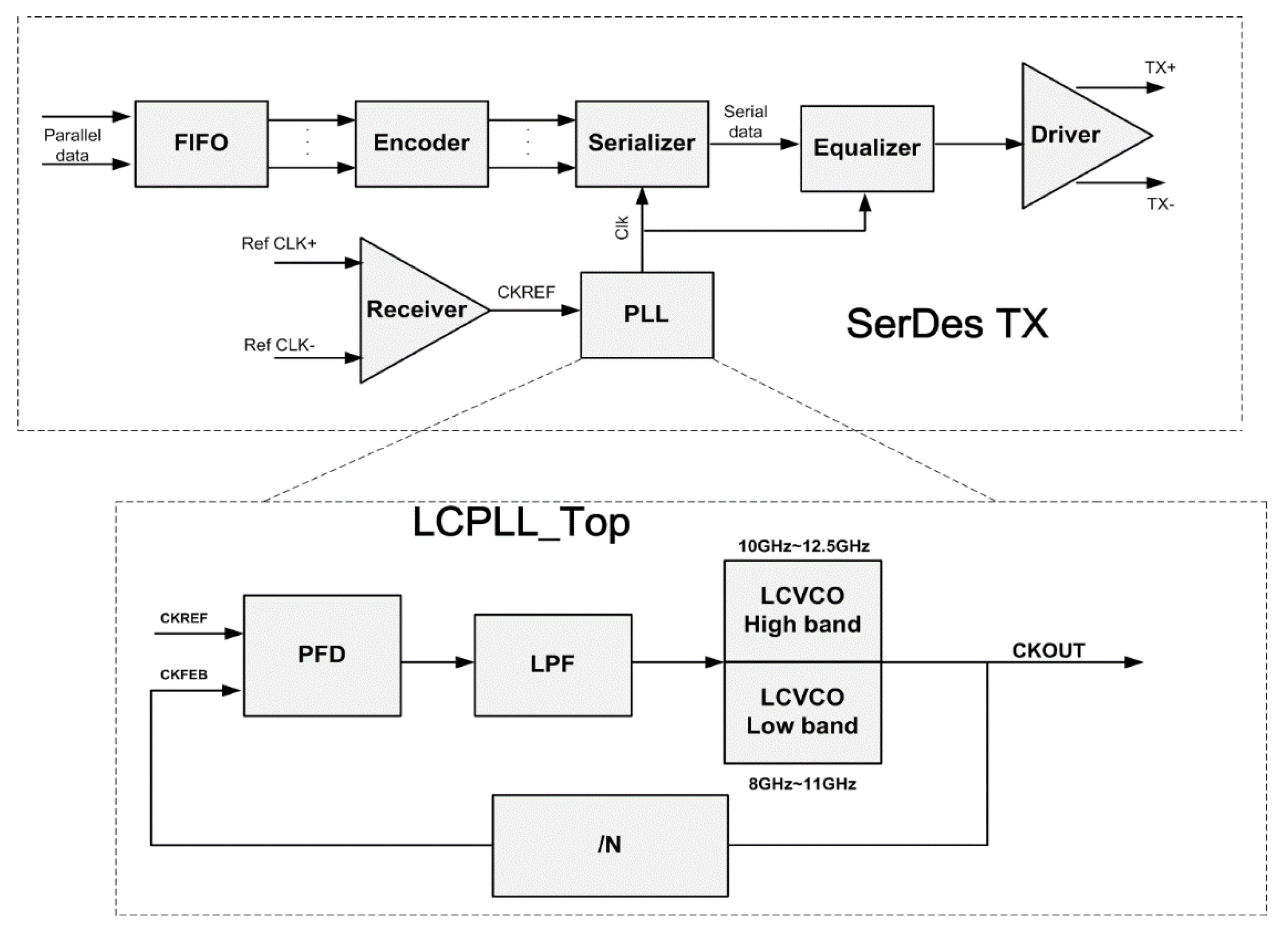
The SerDes transmitter (TX) structures are shown in Figure 1. They include a first-in first-out (FIFO) memory, which is used to synchronize different input data. The encoder can encode the data into the SerDes standard. The serializer can convert data of the parallel format into data of the serial format. The equalizer is used to improve the high-frequency component in the serial data to compensate the high-frequency energy loss in the transmission channel. The driver can improve the driving ability of serial data. The serializer needs a high-frequency and low-jitter clock input, which is usually provided by a PLL. The receiver can change the input differential clock signal Ref CLK+ and Ref CLK− into a single-ended clock signal reference clock (CKREF) and provide this CKREF to the PLL as an input reference clock signal.
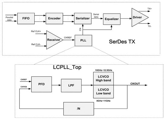
Figure 1.
Block diagram of the Serdes transmitter (TX) and the inductance capacitance (LC) phase-locked loop (PLL) structure. FIFO: first-in first-out; PFD: phase and frequency detector; LPF: low pass filter.
The LC PLL structure is also shown in Figure 1. It includes a phase and frequency detector (PFD), which is used to detect the phase and frequency difference between the CKREF and feedback clock (CKFEB) signals. The PFD output is mostly a narrow pulse signal. The low pass filter (LPF) can convert the PFD output signal into a smooth analog voltage; the LC VCO output frequency is controlled by the LPF output voltage. For example, if the frequency of CKREF is higher than that of CKFEB, the LPF output voltage level and the LC VCO output frequency rise until the frequency of CKFEB is close enough to that of CKREF. When the PLL enters the steady state, the frequency of CKOUT is equal to N*CKREF; therefore, PLL is also used as a frequency multiplier to generate a high-frequency and low-jitter clock signal. The tuning range of the LC VCO is smaller than that of other VCO structures. Therefore, in this study, we designed two LC VCOs covering the range of 8–12.5 GHz and the input CKREF that covers 100 MHz, which can meet most clock applications.
The main module of the LC PLL shown in Figure 1 is the LC VCO, which is also the main source of noise in the LC PLL. The noise of the LC VCO can be divided into two parts: one is the device noise of the LC VCO itself and the other is the coupling noise from the power source. Thus, the noise reduction of the LC VCO often focuses on two parts: reducing the device noise and the power coupling noise. This study mainly focuses on reducing the power coupling noise. The proposed design uses LDO as a power supply to the LC VCO, which can effectively reduce the power coupling noise. However, the device noise of LDO itself is simultaneously introduced into the VCO output frequency. To meet the noise requirements of the LC PLL and LC VCO, the proposed design also adopts an LDO structure that can effectively reduce the LDO device noise.
2.2. LC VCO Structure and Noise Analysis
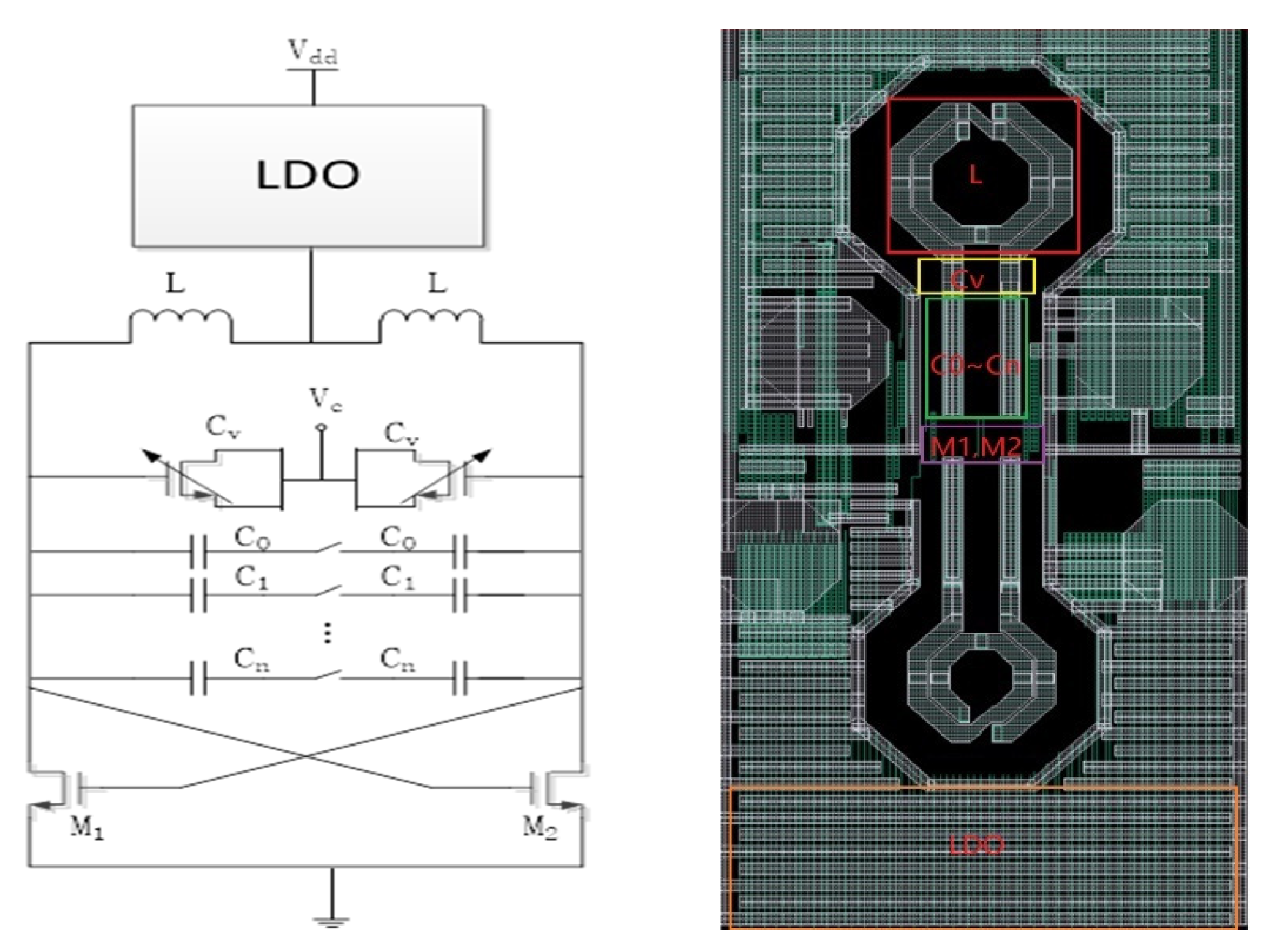
For a PLL system, the phase noise of the VCO is the key factor determining the clock jitter of the entire PLL. Figure 2 shows the LC VCO circuit structure and passive inductance layout designed by the metal layer. The LC VCO mainly comprises an on-chip inductance L, a voltage-controlled capacitance array Cv and C0–Cn, and an LDO. The layout should be highly symmetrical to reduce the parasitic effect. Both the voltage-controlled capacitance and on-chip inductance are not the main sources of noise. The voltage-controlled capacitance array determines the tuning range of the LC VCO output frequency. The LDO isolates most of the noise from the 1.8-V power supply VDD and provides a 1.1-V low-noise power supply to the VCO. This reduces the phase noise of the VCO output frequency. In the circuit, as shown in Figure 2, we only use two cross-coupled N-metal-oxide-semiconductors (NMOSs), M1 and M2, to provide current to the LC oscillator, rather than the current source circuit, because the LDO not only suppresses the power noise but also limits the total current provided to the LC oscillator to achieve stable oscillation. Such an LC VCO design simplifies the active devices in the circuit and can also achieve better phase noise.
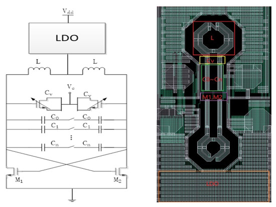
Figure 2.
LC voltage-controlled oscillator (VCO) structure and passive inductance layout. LDO: low dropout regulator.
The phase noise of the LC VCO is the most important parameter for measuring VCO performance. There are several models and theories for analyzing phase noise, among which the Leeson model formula is widely used [19,20]:
where is the VCO oscillation frequency, is the frequency offset, is the signal power, is the Boltzmann constant, is the temperature in Kelvin, and is the noise factor, which is an empirical parameter usually obtained through an experimental fitting. is the turn-around frequency of and , and in this Leeson model, it is equal to the inflection point of the device noise. Q is the quality factor of the LC oscillator. Sometimes, measurement data did not match this Leeson formula very well, because Leeson formula is a fitting formula, but it also can give some important guidance to low noise VCO design. As shown in Formula (1), increasing the signal power and the value, as well as decreasing the boundary frequency and noise factor , can effectively reduce the VCO output frequency phase noise. The mechanism of noise factor is very complex, mainly due to the variable capacitance and differential pair.
In the proposed design, the LDO is used to isolate power supply noise; thus, the total noise output by the LC VCO includes the noise of the LDO and LC VCO devices. Because there is no correlation between the LC VCO and LDO device noises, the total phase noise of the LC VCO can be expressed as Formula (2):
where is the total output phase noise of the LC VCO at a frequency offset and is the device noise of the LC VCO itself at a frequency offset ; is the LDO output noise at a frequency offset . In this study, we measured the VCO phase noise at = 1 MHz. When we consider the influence of the VCO power supply on the VCO output frequency phase noise because the VCO power supply is provided by the LDO output voltage in this design, the LDO output noise can equivalently be expressed as Formula (3) [21]:
where is the offset frequency (Hz) corresponding to the measurement of noise spectral density, is the noise spectral density () of the LDO output, and is the voltage push coefficient (MHz/V) of the VCO, which is used to represent the disturbance caused by the power supply voltage fluctuation to the VCO output signal frequency.
The LDO output voltage in this design is 1.1 V. Accordingly, we use an ideal power supply for the LC VCO and set the supply voltage to 1.1 ; under this condition, the simulated voltage push coefficient P of the LC VCO is approximately 490 MHz/V, implying that when the supply voltage changes to 0.05 V, the LC VCO output frequency changes by approximately (490 MHz/V) × 0.05 V = 24.5 MHz. The LC VCO phase noise simulation result is −108.7 dBc/Hz at 1MHz with the ideal power supply at 1.1 V. The SerDes system requires that the LC VCO total phase noise SPEC be less than −105 dBc/Hz at 1MHz. According to formulas (2) and (3), at fm = 1 MHz, the calculation result of LDO noise spectral density should be less than 12 nV/ to meet the SPEC. The noise characteristics of a traditional LDO and this design LDO are analyzed below.
2.3. Noise-Reduced LDO Design
The main noise in a traditional LC PLL comes from the LC VCO. In SerDes applications, to avoid the interference of the TX, Receiver (RX), and other digital modules, an LDO is placed on the LC VCO to isolate the noise interference from the power supply. However, the LDO also brings its noise, which is modulated by the VCO circuit to the VCO output frequency and becomes VCO phase noise. Thus, reducing LDO noise has become a key point of low-noise LC VCO design.
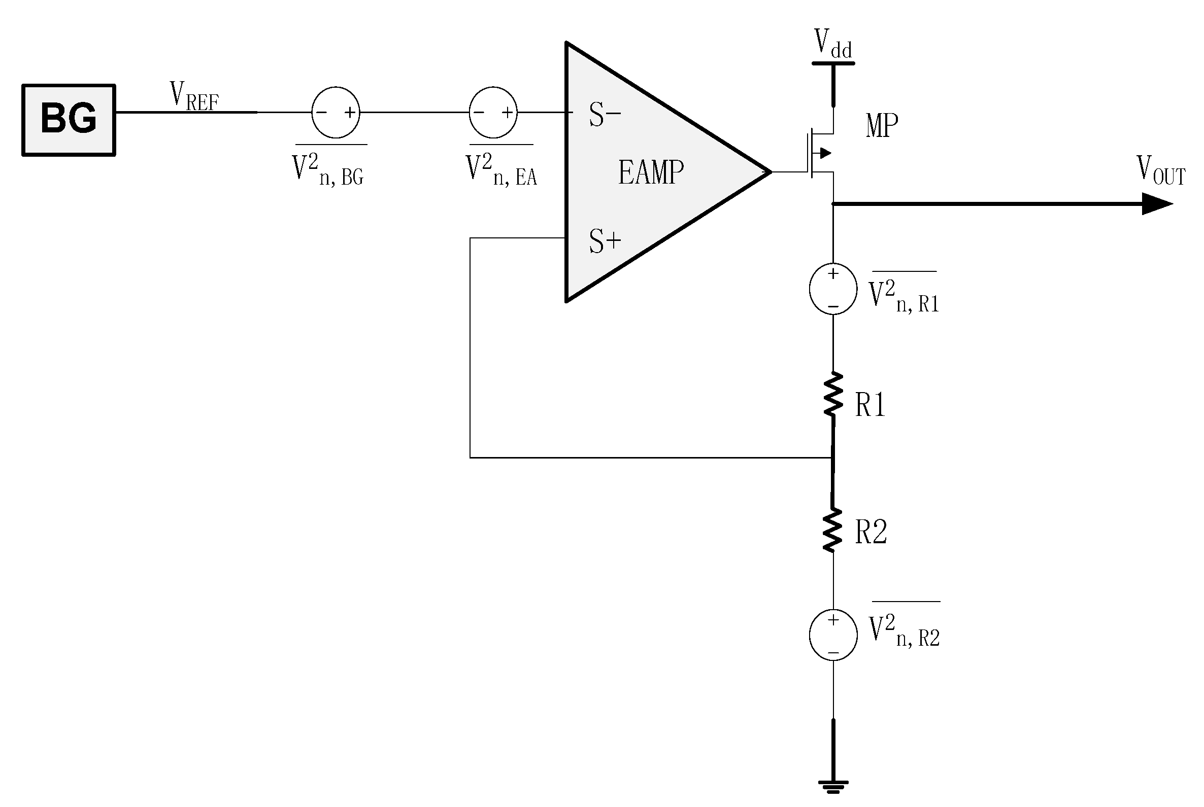
The traditional LDO structure is shown in Figure 3. According to the circuit principle, the output voltage of the traditional LDO can be calculated as follows:

Figure 3.
Conventional low-dropout (LDO) regulator structure. BG: bandgap reference.
The output noise of the traditional LDO comprises three parts: the output noise of bandgap reference (BG) , equivalent input noise of the error amplifier (EAMP) , and thermal noise of the resistance feedback network and . These noises are uncorrelated and can be accumulated. Thus, the equivalent output noise of the traditional LDO (with a frequency range of ) is [22]:
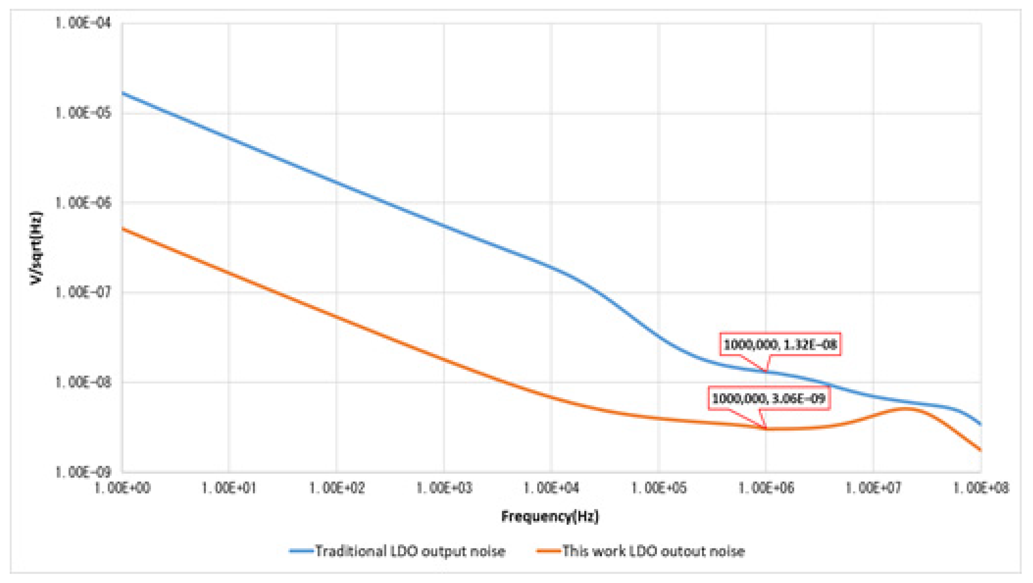
According to the above calculation, the noise performance requirement of the SerDes system in this LDO design is less than 12 nV/ at 1 MHz. But the simulation result of the output noise performance of the traditional LDO structure is 13.2 nV/ at 1 MHz, which cannot meet the requirements of less than 12 nV/ at 1 MHz. However, it is difficult to reduce the noise caused by BG and EAMP, which usually requires an RC filter with a low inflection point to remove the device noise, but this will result in an extremely large area.
In the design of an LDO, digital feedback control and programmable technology are often introduced to optimize the performance of the LDO. Huang and Liao [23] used programmable feedback resistance to considerably expand the output voltage range of the LDO. Yuan et al. [24] used a digital feedback control technology to reduce the ripple and dropout voltage of LDO output. The LDO in the present study used the digital control algorithm finite state machine (FSM) to reduce LDO device noise.
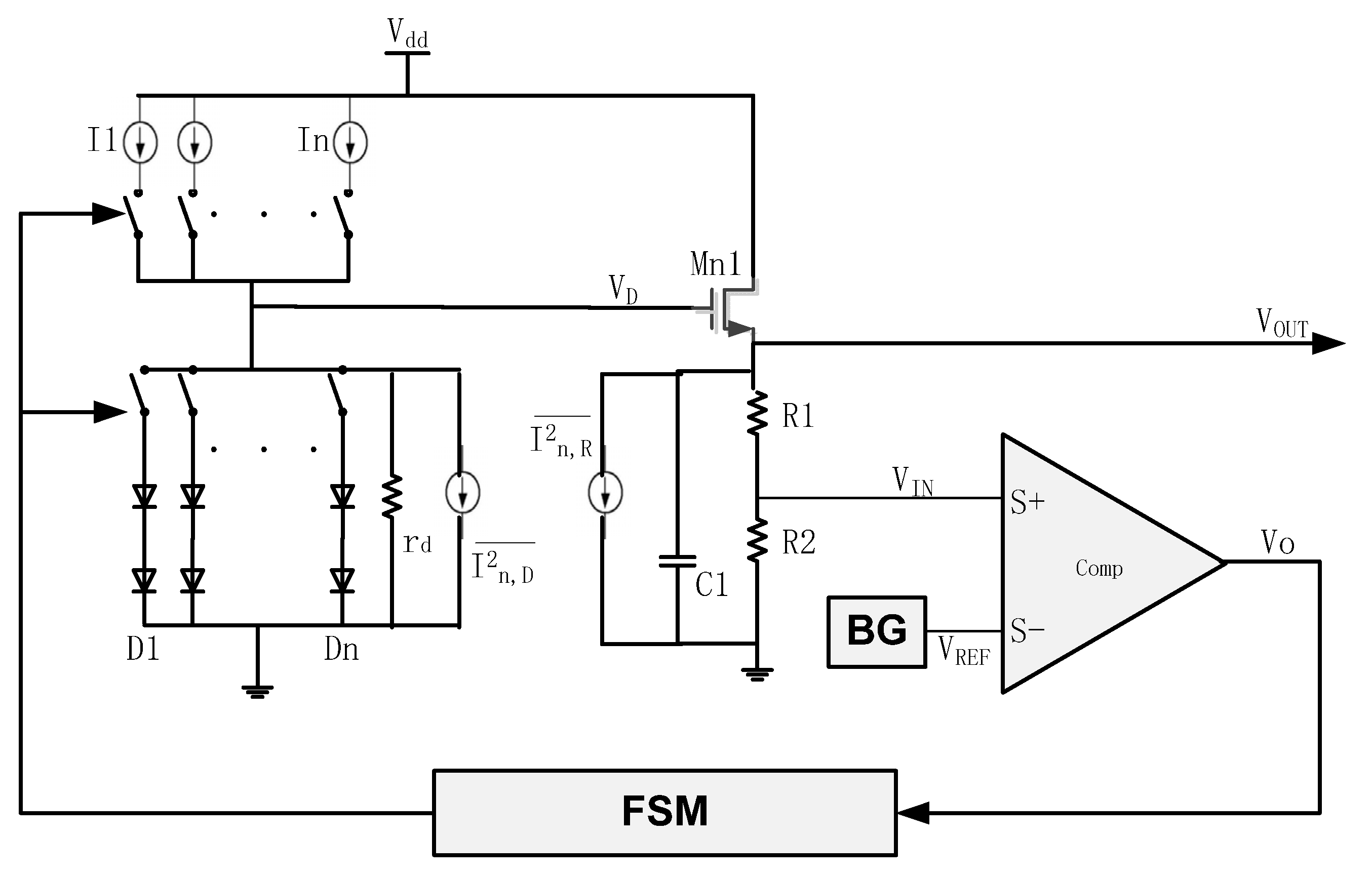
The LDO structure in this study is shown in Figure 4. Compared with the traditional structure, it comprises a current source array I1–In, a diode array D1–Dn, a comparator (Comp), a BG that is not in the loop, and an FSM.

Figure 4.
Structure of the noise-reduced LDO regulator. FSM: finite state machine.
Current source I1–In generates controllable current according to different switch control signals, which is input into the diode array D1–Dn, and a voltage VD is generated at the gate of Mn1, which is a source follower. The voltage drops from VD to . Then, =)/(R1 + R2) is compared with VREF, which is generated by a BG, and the comparison result Vo is input into the control algorithm FSM. If Vo is 1, it indicates that the output voltage (VOUT) is greater than the expected voltage (VREF) × (R1 + R2)/R2 and the output of the control algorithm FSM reduces the current source array, thus reducing VOUT. If Vo is 0, it indicates that VOUT is less than the expected voltage VREF × (R1+R2)/R2, and the output of the control algorithm FSM increases the current source array, thus increasing VOUT. The output of the control algorithm FSM can control both the current source array and the diode array, and the principle of controlling the current source array and the diode array is similar. Moreover, it is possible to control both the current source and diode array simultaneously, with one array as rough tuning and the other as fine tuning; the tuning precision determines the voltage precision of the final LDO output. When the mean value of Vo in a continuous time is close to 0.5, the loop is considered to have entered a stable state. At this point, the loop is cut off and the output value of the FSM and VOUT is fixed. In this way, BG noise will not enter the loop after the control algorithm loop is disconnected, thus eliminating the influence of BG noise on LDO output VOUT. In addition, because of the diode being a device that is below the gate surface, the diode noise is smaller than that of the conventional CMOS device; thus, the noise generated by the analog circuit in the entire loop is smaller than that of the bandgap voltage source BG and EAMP in the conventional architecture.
The output noise of the noise-reduced LDO regulator in this design can be expressed as follows:
When the algorithm control loop is disconnected, R = R1 + R2, rd is the equivalent dynamic resistance of the diode array and is the static current of the diode array. Compared with the traditional structure LDO, the noise from BG and EAMP is suppressed and the diode itself has low noise; therefore, the noise performance improves significantly.
The simulation results of the noise-reduced LDO regulator output of this design are also shown in Figure 5. The noise is 3.06 nV/ at 1 MHz, which fully meets the requirement of 12 nV/ at 1 MHz.
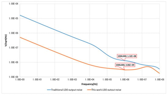
Figure 5.
Comparison of output noise simulation results of the conventional LDO and the proposed LDO.
In this study, we used Cadence (Cadence Systems, Inc., San Jose, CA, USA) Spectre as the circuit simulation tool; the AC noise analysis function in the Cadence Spectre tool was chosen to evaluate the LDO output noise spectral density. This design is based on the UMC 28-nm 1P10M CMOS technology; the device noise parameters are included in the model file of the UMC 28-nm 1P10M CMOS technology, which loads in the Cadence Spectre tool during the simulation.
3. Post-Simulation and Measurement Results
3.1. Low-Noise LC PLL Layout
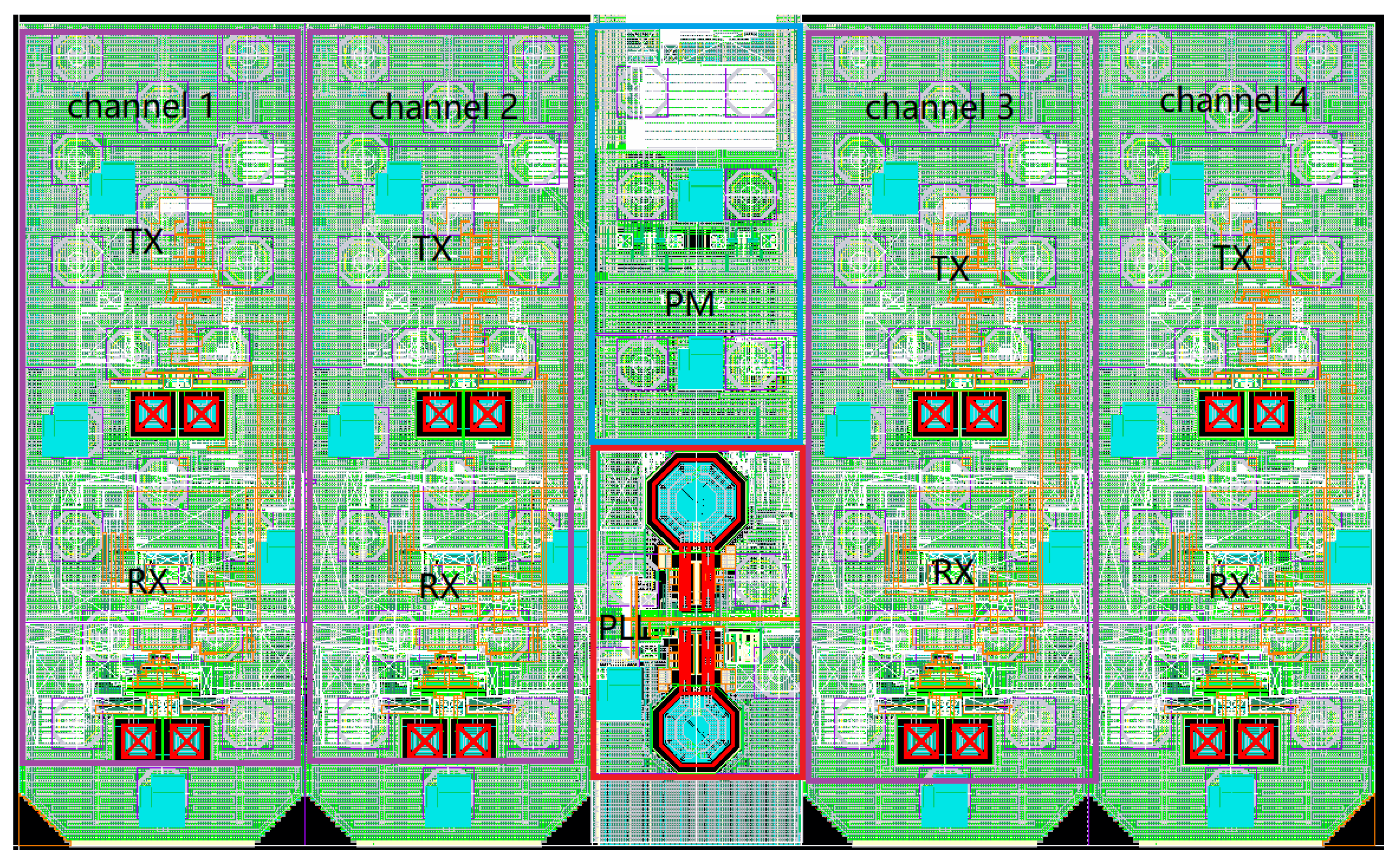
Figure 6 shows the four-channel SerDes system layout using the LC PLL of the proposed design. The red rectangular region is the LC PLL. The blue rectangular region is the power management (PM) circuit. The four purple rectangular regions are the four channels of the SerDes TX and RX. The LC PLL is based on the UMC 28-nm 1P10M CMOS technology, and the LC PLL area is .
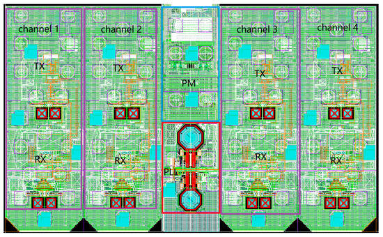
Figure 6.
Layout of SerDes and PLL. RX: Receiver; PM: power management.
3.2. VCO Noise
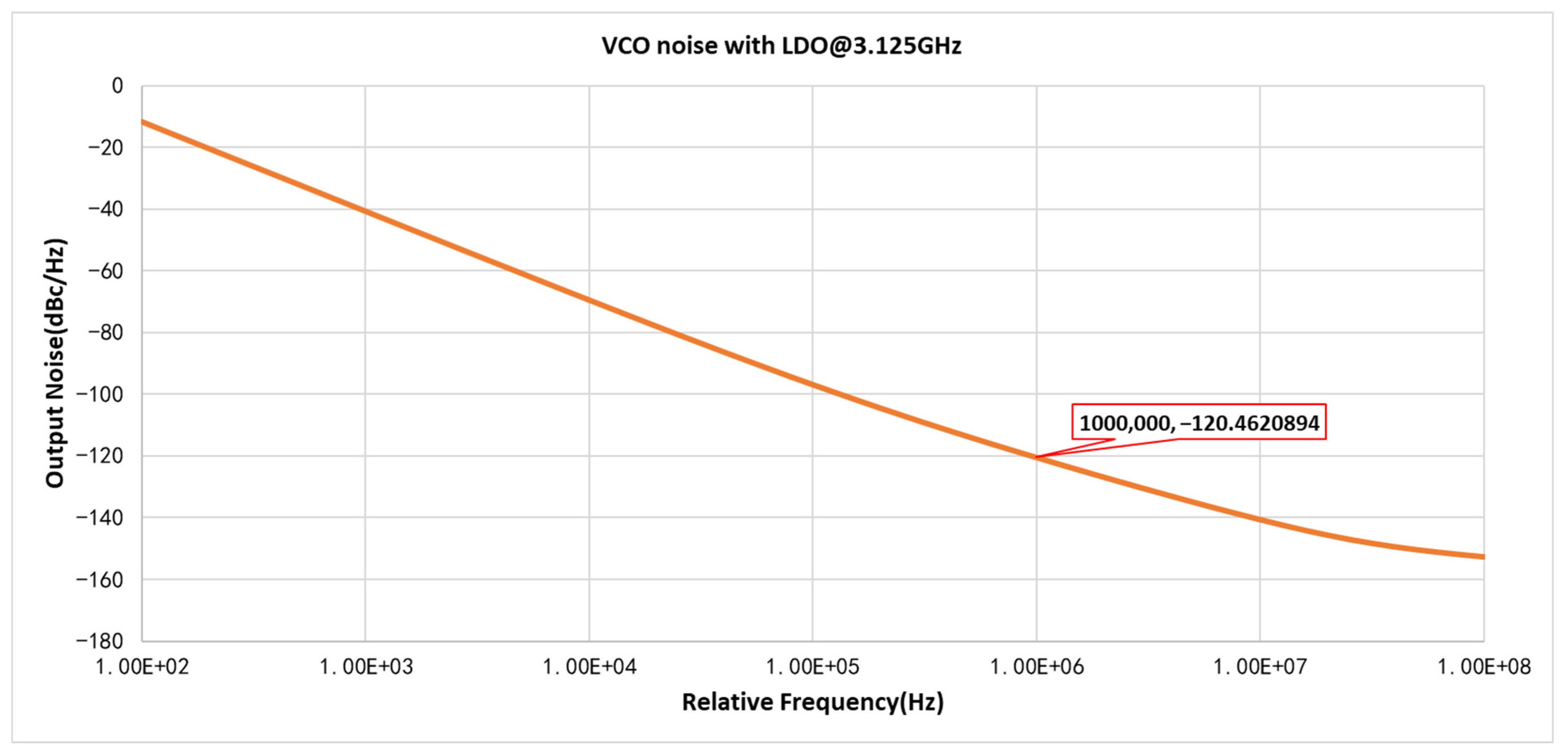
Figure 7 shows the post-simulation result of the total output phase noise of the LC VCO designed in this study. It should be noted that to correspond to the test circuit, during the simulation, the output frequency of the VCO should be 3.125 GHz after passing through a divide-by-four circuit (the frequency is reduced four times). The phase noise simulation result includes the influence of the VCO’s device and LDO output noises.
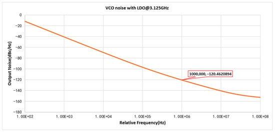
Figure 7.
LC VCO output phase noise post-simulation results.
The post-simulation result in Figure 7 shows that when the LC VCO output frequency is divided by 12.5–3.125 GHz, the phase noise is −120.46 dBc/Hz at a frequency offset fm = 1 MHz. The simulation tool is also a Cadence Spectre; the PSS and P noise function in the Spectre tool were chosen for the oscillation signal analysis.
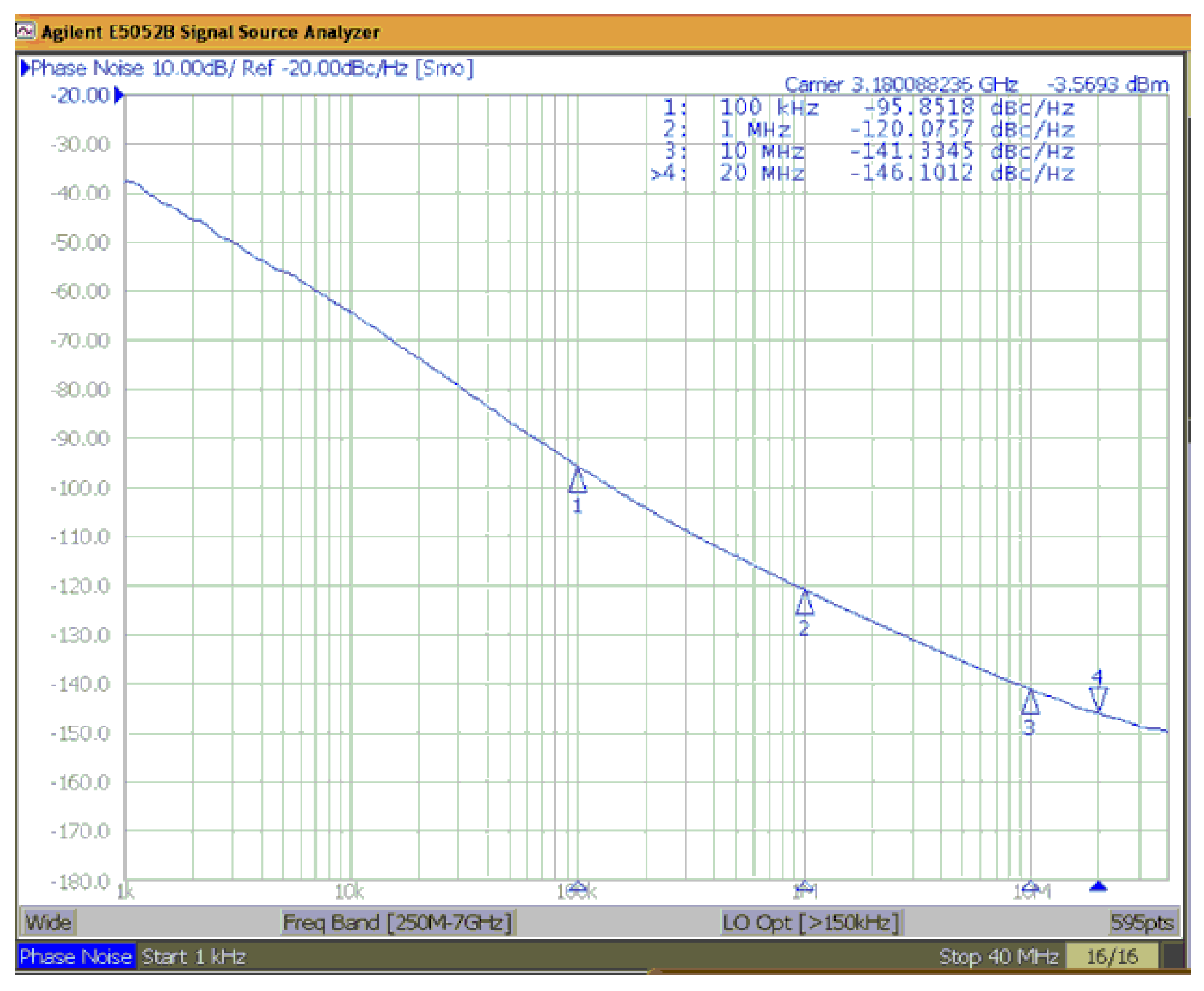
Figure 8 shows the LC VCO output phase noise test results in the open-loop condition. The LC VCO output frequency is passed through the divide-by-four test circuit, and the noise spectrum of LC VCO is free run at 3.18 GHz, measured using E5052B, which is a signal source phase noise analyzer manufactured by Agilent (Agilent Technologies Inc., Santa Clara, CA, USA).
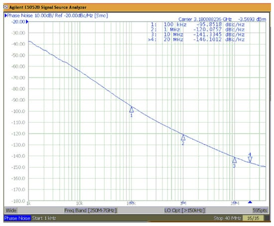
Figure 8.
Test results of VCO output.
The post-simulation and test results in Figure 7 and Figure 8 are very close, −120.46 and −120.08 dBc/Hz, respectively, at a 1-MHz frequency offset. Because the output frequency of the VCO at this time is reduced by four times after a divide-by-four circuit, it can be calculated according to the fact that the phase noise around 12.5 GHz will worsen by approximately 12 dBc/Hz compared with the above results around 3.125 GHz. In particular, when the output frequency is 12.5 GHz and the frequency offset is 1 MHz, the phase noise is approximately −108.46 and −108.08 dBc/Hz, respectively. This test result meets the requirement that the phase noise of LC VCO output should be less than −105 dBc/Hz at 1 MHz when the output frequency is 12.5 GHz. The abovementioned test and post-simulation conditions are obtained with a 1.8 V power supply at 27 °C, with a TT device. TT means that the process corner is a typical NMOS device and a typical P-channel metal oxide semiconductor (PMOS) device.
3.3. LC PLL Noise
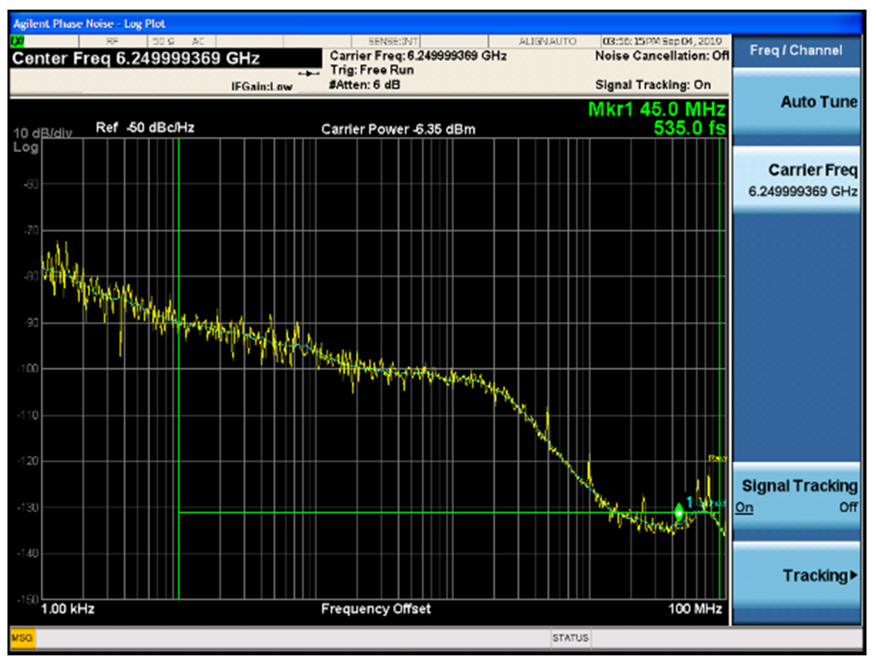
The LC PLL and LC VCO test system block diagram is shown in Figure 9, and the noise spectrum test results of the LC PLL output at 12.5 GHz are shown in Figure 10.
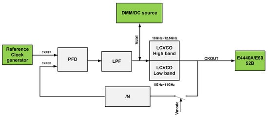
Figure 9.
Block diagram of the LC PLL and LC VCO test system.
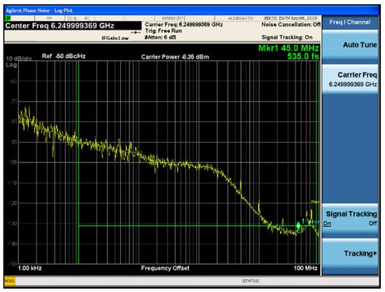
Figure 10.
LC PLL output noise test results.
The PLL test system shown in Figure 9 can test both the LC VCO and LC PLL output noise performance. To test the LC PLL, Vmode was set to make the loop close and a Digital Multimeter (DMM) was used to monitor the Vctrl voltage from the LPF output. If Vctrl becomes stable, it means the LC PLL has also entered a stable state; in that case, E4440A is used to test the LC PLL output frequency jitter. E4440A is a spectrum analyzer manufactured by Agilent Technologies Inc. To test the LC VCO, Vmode was set to make the loop open, and a DC source was used to supply an external Vctrl to the LC VCO. Then, the E5052B was used to test the LC VCO output frequency phase noise.
When the PLL output is 12.5 GHz, the period is 80 ps and the maximum random jitter tolerance is approximately 8 ps, which should satisfy the seven-sigma standard; thus, the maximum jitter spec for PLL is 8 ps/14 = 0.571 ps. Test results show that the PLL jitter in this study is 0.535 ps.
In this design, the noise jitter spec of the LC PLL is 0.571 ps (integral range of 1 KHz–20 MHz), and the test result shown in Figure 10 is 0.535 ps (integral range of 1 KHz–90 MHz). The test result meets the spec requirements.
3.4. Calculation of the LC VCO Figure of Merit (FOM) Value
The designed LC VCO works at 1.1 V with an average operating current of 3 mA and power consumption of 3.3 mW. The calculation formula of FOM [25] value is as follows:
where is the phase noise of the LC VCO; is the frequency offset, which is 1 MHz here; is the central frequency of LC VCO output; P is the power consumption of the LC VCO. Based on the above data, the calculated FOM value of the LC VCO in this design is 185 dB. The results of the comparison between the calculated FOM value in this work and the FOM value of VCOs in some references are given in Table 1; our FOM value is better than those of some references [25,26], and our is much higher than that of [27]; thus, the present study achieves a better trade-off between the and FOM value.

Table 1.
Comparison results of VCO’s Figure of Merit (FOM).
3.5. Performance Summary
The main specs of the VCO and PLL are summarized in Table 2. The simulation results show that the output noise of the LDO in this study is only 3.06 nV/ at 1 MHz (Figure 5). Through the above noise optimization, the total output phase noise test result of the LC VCO is 108.1 dBc/Hz at 1 MHz, the FOM value is 185, and the output noise jitter test result of the LC PLL is 0.535 ps (integral range of 1 KHz–90 MHz), all meeting the spec requirements of the SerDes system. The LC PLL is designed based on the UMC 28-nm CMOS 1P10M technology, and the area is approximately 0.25 mm2. The supply voltage is 1.8 V and the LDO output voltage is 1.1 V. The PLL power consumption is 16.5 mW.

Table 2.
Performance summary of LC PLL and LC VCO.
4. Conclusions
The LC PLL designed in this study was applied to a multilane multiprotocol SerDes system. We designed a dual LC VCO containing a voltage-controlled capacitor array, which can improve the coverage of the LC VCO output frequency; a further improvement was achieved by designing a new low-noise LDO regulator structure (Figure 4). It mainly includes a low-noise diode array and a control algorithm circuit. This low-noise LDO is used as a 1.1-V low-noise power supply for the LC VCO to isolate the noise from the 1.8-V power supply. The diode device noise is much smaller than the CMOS device and this LDO output noise does not contain the BG and EAMP noise; therefore, the total noise of this LDO output is very low. After optimizing the LDO noise performance, the VCO and PLL output noise can meet the spec requirements of the SerDes system.
The designed low-noise LDO can easily reduce the area and power consumption when transferred to 14- or even 7-nm technology. Because a critical analog circuit, which includes low-noise BG and low-noise EAMP, is not necessary for this LDO structure, it can also be used in a high-performance SerDes system based on the 14- or 7-nm technology in the future.
Author Contributions
Methodology, J.C. and Q.S.; software, J.C.; validation, W.Z.; formal analysis, L.L. and J.C.; investigation, L.L. and J.C.; resources, W.Z.; writing—original draft preparation, J.C.; writing—review and editing, L.L.; supervision, W.Z.; project administration, W.Z.; funding acquisition, L.L. All authors have read and agreed to the published version of the manuscript.
Funding
This study has been partially sponsored by the China Postdoctoral Science Foundation, Grant No. 2020M670993.
Data Availability Statement
No new data were created or analyzed in this study. Data sharing is not applicable to this article.
Conflicts of Interest
There are no commercial interests of the authors relevant to the subject of the manuscript; no conflicts of interest exist, and this study has not been submitted elsewhere.
References
- Cevrero, A.; Ozkaya, I.; Francese, P.A.; Brandli, M.; Menolfi, C.; Morf, T.; Kossel, M.; Kull, L.; Luu, D.; Dazzi, M.; et al. A 100Gb/s 1.1pJ/b PAM-4 RX with Dual-Mode 1-Tap PAM-4/3-Tap NRZ Speculative DFE in14 nm CMOS FinFET. In Proceedings of the 2019 IEEE International Solid-State Circuits Conference (ISSCC), San Francisco, CA, USA, 17–21 February 2019; pp. 112–113. [Google Scholar]
- LaCroix, M.-A.; Wong, H.; Hua, Y.L.; Ho, H.; Lebedev, S.; Krotnev, P.; Nicolescu, D.A.; Petrov, D.; Carvalho, C.; Alie, S.; et al. A 60Gb/s PAM-4 ADC-DSP Transceiverin 7 nm CMOS with SNR-Based Adaptive Power ScalingAchieving 6.9 pJ/b at 32dB Loss. In Proceedings of the 2019 IEEE International Solid-State Circuits Conference (ISSCC), San Francisco, CA, USA, 17–21 February 2019; pp. 114–116. [Google Scholar]
- Hong, J.-P. A low supply voltage and wide-tuned CMOS Colpitts VCO. IEICE Electron. Express 2014, 11, 20140428. [Google Scholar] [CrossRef][Green Version]
- Wang, T.-P.; Chiang, C.-Y. A low-power low-phase-noise wide-tuning-range K-band VCO in 0.18 μm CMOS. IEICE Electron. Express 2011, 8, 1511–1518. [Google Scholar] [CrossRef]
- Cameron, R.J.; Yu, M.; Wang, Y. Direct-coupled microwave filters with single and dual stopbands. IEEE Trans. Microw. Theory Tech. 2005, 53, 3288. [Google Scholar] [CrossRef]
- Noruzpur, F.; Mahdavi, S.; Poreh, M.; Ghasemi, S.T. A New Semi-Digital Low Power Low Jitter and Fast PLL in 0.18 μm Technology. In Proceedings of the 2018 25th International Conference Mixed Design of Integrated Circuits and System (MIXDES), Gdynia, Poland, 21–23 June 2018. [Google Scholar]
- Gao, X. Low jitter and low power PLL: Towards the Utopia. In Proceedings of the 2019 International SoC Design Conference (ISOCC), Jeju, Korea, 6–9 October 2019; pp. 2163–9612. [Google Scholar]
- Ebrahimi, E.; Naseh, S. A new low-phase noise direct-coupled CMOS LC-QVCO. IEICE Electron. Express 2009, 6, 1337–1344. [Google Scholar] [CrossRef]
- Yang, Z.-Y.; Chen, R.Y. High-performance cost-efficient dual-band CMOS LC VCO. IEICE Electron. Express 2015, 12, 20150118. [Google Scholar] [CrossRef][Green Version]
- Kim, J.; Park, J.; Kim, J. A Low Phase Noise 0.9–1.8 GHz Dual-band LC VCO in 0.18 μm CMOS Technology. In Proceedings of the 2018 International Conference on Electronics, Information, and Communication (ICEIC), Honolulu, HI, USA, 24–27 January 2018; ISBN 978-1-5386-4754-7. [Google Scholar]
- Sunil, B.; Kulkarni, N.B.; Pradeep, P.; Praveen, P.K.; Singh, B.K.; Chippalkatti, V. Design of Low Noise and Low Power LDO for Senor Application. In Proceedings of the International Conference on Smart Technologies in Computing, Electrical and Electronics (ICSTCEE 2020), Bengaluru, India, 9–10 October 2020. [Google Scholar] [CrossRef]
- Xingrun, B.; Fei, X. Research on ultra-low noise LDO measurement technology. In Proceedings of the 2020 21st International Conference on Electronic Packaging Technology (ICEPT), Guangzhou, China, 12–15 August 2020; pp. 1–4. [Google Scholar]
- Chang, M.; Liu, L.; Mu, J. A Low Noise LDO with Pre-amplified Stage and Base-current Compensation. In Proceedings of the 2018 14th IEEE International Conference on Solid-State and Integrated Circuit Technology (ICSICT), Qingdao, China, 31 October–3 November 2018; pp. 1–4. [Google Scholar]
- Zheng, X.; Feng, H.; Zhang, N. An External Capacitorless Low-Dropout Regulator with 5.58 μV Integrated Output Noise from 10 Hz to 100 kHz Using Adaptive Bias Technique. In Proceedings of the 2020 IEEE 3rd International Conference on Electronics Technology (ICET), Chengdu, China, 8–11 May 2020; pp. 242–246. [Google Scholar]
- Hou, W.; Li, S.; De Geronimo, G.; Stanacevic, M. An Ultra-Low-Noise LDO Regulator in 65 nm for Analog Front-End ASICs in Cryogenic Environment. In Proceedings of the 2018 IEEE Nuclear Science Symposium and Medical Imaging Conference Proceedings (NSS/MIC), Sydney, Australia, 10–17 November 2018; pp. 1–4. [Google Scholar]
- Wang, J.-P.; Jiang, J.-G.; Zhou, X.-F. Less occupied and ultra-low noise LDO design. Analog. Integr. Circuits Signal. Process. 2014, 81, 453–459. [Google Scholar] [CrossRef]
- Abbasizadeh, H.; Rikan, B.S.; Nga, T.T.K.; Kim, K.-T.; Kim, S.; Lee, D.-S.; Lee, K.-Y. A design of ultra-low noise LDO using noise reduction network techniques. In Proceedings of the 2017 International SoC Design Conference (ISOCC), Seoul, Korea, 5–8 November 2017; pp. 198–199. [Google Scholar]
- Magod, R.; Suda, N.; Balasingam, R.; Bakkaloglu, B. A Low Noise Output Capacitor-less Low Dropout Regulator with a Switched-RC Bandgap Reference. IEEE Trans. Power Electron. 2017, 32. [Google Scholar] [CrossRef]
- Barnes, J.A.; Chi, A.R.; Cutler, L.S.; Healey, D.J.; Leeson, D.B.; McGunigal, T.E.; Mullen, J.A.; Smith, W.L.; Sydnor, R.L.; Vessot, R.F.; et al. Characterization of Frequency Stability. IEEE Trans. Instr. Meas. 1971, 20, 105–120. [Google Scholar] [CrossRef]
- Rutman, J. Characterization of Phase and Frequency Instabilities in Precision Frequency Source: Fifteen Years of Progress. Proc. IEEE 1978, 66, 1048–1075. [Google Scholar] [CrossRef]
- Basso, C.; Fourtet, C.; Kadanka, P. Get the beat from your low-dropout regulator. EDA 1999, 44, 115–226. [Google Scholar]
- Li, Q.; Jiang, J.; Wang, J.; Gong, X.; Zhou, X.; Li, S. A CMOS low-noise, low-dropout regulator. In Proceedings of the Asia-Pacific Power and Energy Engineering Conference, Chengdu, China, 28–31 March 2010; pp. 1–4. [Google Scholar]
- Huang, C.-H.; Liao, W.-C. A compact programmable LDO regulator for ultra-low voltage SoC. IEICE Electron. Express 2014, 11, 20140820. [Google Scholar] [CrossRef][Green Version]
- Yuan, W.; Chen, X.; Yan, N.; Wang, Y.; Min, H. An LDO regulated DC-DC converter with voltage ripple suppression and adaptive dropout voltage control. IEICE Electron. Express 2018, 15, 20180651. [Google Scholar] [CrossRef]
- Cheng, K.-H.; Hung, C.-L.; Gong, C.-S.A.; Liu, J.-C.; Jiang, B.-Q.; Sun, S.-Y.; Cheng, K.-H.; Hung, C.-L.; Gong, C.-S.A.; Liu, J.-C.; et al. A 0.9- to 8-GHz VCO with a Differential Active Inductor for Multistandard Wireline SerDes. IEEE Trans. Circuits Syst. II Express Briefs 2014, 61, 559–563. [Google Scholar] [CrossRef]
- Min, S.; Copani, T.; Kiaei, S.; Bakkaloglu, B. A 90-nm CMOS 5-GHz ring-oscillator PLL with delay-discriminator-based active phasenoise cancellation. IEEE J. Solid-State Circuits 2013, 48, 1151–1160. [Google Scholar] [CrossRef]
- Khan, A.B.; Cardenas, J.; Chen, L.; Khan, M.; Qureshi, A. A Low Power and Low Noise Voltage-Controlled Oscillator in 28-nm FDSOI Technology for Wireless Communication Applications. In Proceedings of the 2019 IEEE Canadian Conference of Electrical and Computer Engineering (CCECE), Edmonton, AB, Canada, 5–8 May 2019. [Google Scholar] [CrossRef]
Publisher’s Note: MDPI stays neutral with regard to jurisdictional claims in published maps and institutional affiliations. |
© 2021 by the authors. Licensee MDPI, Basel, Switzerland. This article is an open access article distributed under the terms and conditions of the Creative Commons Attribution (CC BY) license (https://creativecommons.org/licenses/by/4.0/).

