Article

Analysis and Modeling of Mueller–Muller Clock and Data Recovery Circuits

1
School of Air and Missile Defense College, Air Force Engineering University, Xi’an 710051, China
2
School of Computer, National University of Defense Technology, Changsha 410003, China
3
Institute of Microelectronics of Chinese Academy of Sciences, Beijing 100029, China
4
School of Information Science and Technology, University of Science and Technology of China, Hefei 230027, China
*
Authors to whom correspondence should be addressed.
Electronics 2021, 10(16), 1888; https://doi.org/10.3390/electronics10161888
Submission received: 24 June 2021 / Revised: 26 July 2021 / Accepted: 3 August 2021 / Published: 6 August 2021
(This article belongs to the Section Microelectronics)

Abstract

:
In this paper, an accurate linear model of the Mueller–Muller phase detector (MMPD)-based clock and data recovery circuit (MM-CDR) is proposed, which analyzes several critical points of the MM-CDR including the linearization of the MMPD and the gain of the voter. Using our technique, the jitter between the recovery clock and the input data can be estimated with a sub-picosecond accuracy, as demonstrated in the simulation results of a 56 Gb/s quarter-rate MM-CDR implemented in 28 nm CMOS.

1. Introduction

With the rapid development of integrated circuits and the emergence of advanced process nodes, the data transfer rate of high-speed serial interfaces (i.e., serializer/deserializer) has grown exponentially [1]. The rapid growth of data rate makes the classical Bang-Bang phase detector (BBPD) no longer suitable for high-speed clock and data recovery (CDR). However, the advantage of the Mueller–Muller phase detector (MMPD) that requires only one sample per symbol alleviates the problem of BBPD timing tension and exponential growth of power consumption in high-speed situations, making Mueller–Muller baud-rate sampling widely used in the serial IO design [2,3,4,5,6].
Compared to the Mueller–Muller baud-rate sampling technique, a lot of work has been done on Bang-Bang CDR. In [7], Jee et al. linearized the BBPD using the effect of metastability and input jitter, combining with the behavioral characteristics of large signals to characterize the jitter transfer and jitter tolerance of the CDR. However, for jitter transfer, we are more concerned about the bandwidth of the CDR after locking (i.e., in a small range). In [8], Sonntag et al. described a linear model for the general architecture of digital clock and data recovery. They linearized the BBPD using Gaussian jitter and derived the gain formula, and then obtained a linear model of the CDR in combination with the analysis of other modules of the digital CDR loop, in which the input jitter of the BBPD needs to be simulated accurately each time. The authors in [9] summarized the existing linear models of BBPD and analyzed the effect of random jitter and finite loop delay on the loop characteristics. Nevertheless, there is no analysis of linearization for the MM-CDRs in previous work, which all focus on the use of the Mueller–Muller baud-rate sampling technique. For example, Dokania et al. [10] introduced an unequalized MM-CDR, which can adjust the phase lock position according to the extracted channel response and achieve the adaptive channel response; while Choi et al. [11] presented a weight-adjusting sign-sign Mueller–Muller clock and data recovery circuit. These studies only apply the MMPD without a systematic analysis of the MM-CDR, affecting the circuit design performance and extending the circuit design cycle. To solve these problems, we propose the gain formula of MMPD for the first time using the jitter characteristics of the input, then give the joint analysis method of voter and MMPD, and finally analyze the error jitter for the overall system. Through the above modeling, we address the theoretical gap and provided the basis for the design for MM-CDR.
In this work, we propose a linear model for a Mueller–Muller CDR. The remainder of this article is organized as follows. Section 2 discusses the working principle of MMPD and presents a linear gain model for it. Section 3 describes the gain model of the MMPD-based voter and builds a small-signal model of the MM-CDR to analyze the jitter tolerance and jitter transfer. Section 4 analyzes the error jitter between recovery clock and input data. Section 5 demonstrates the simulation results that validate the analysis of Section 4, and Section 6 draws the conclusion.

2. Mueller–Muller Phase Detector

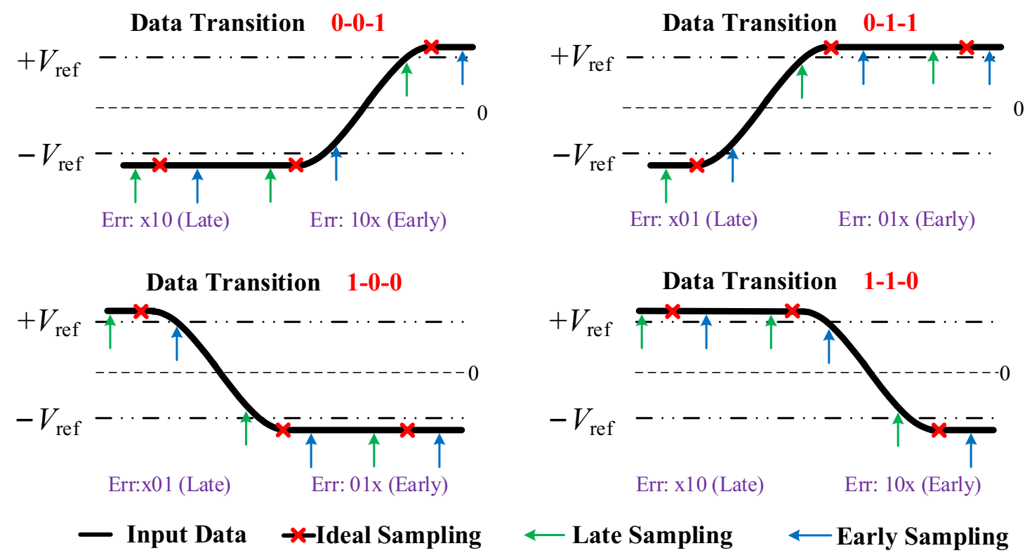
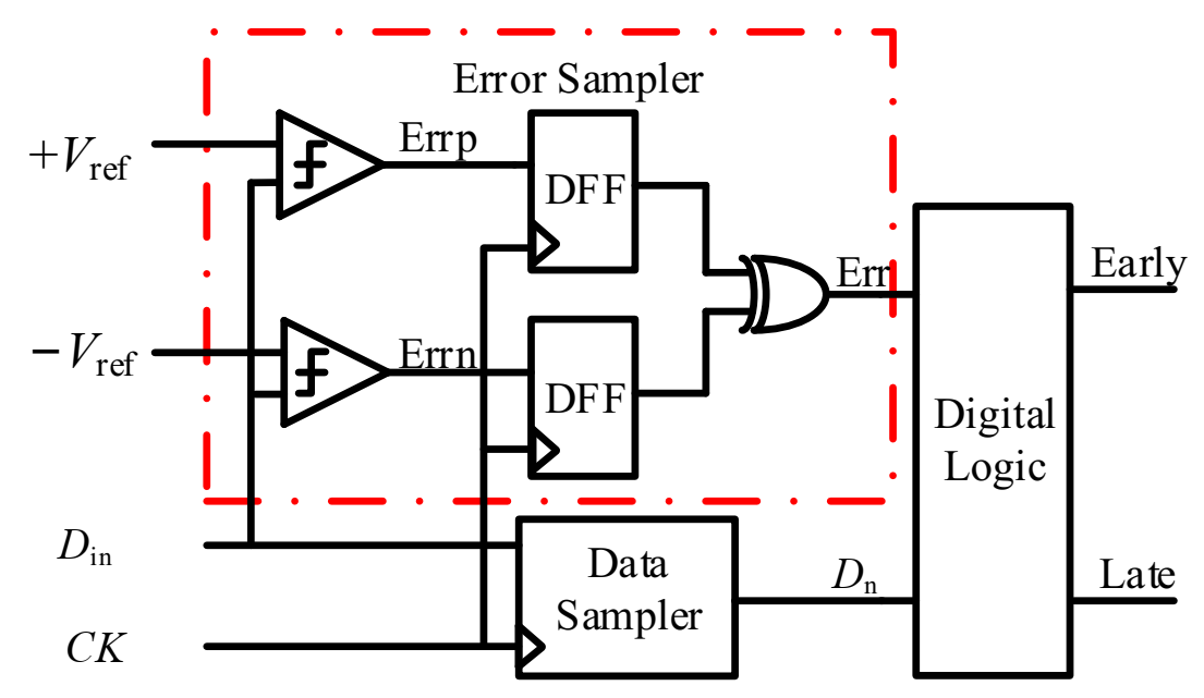
2.1. Working Principle of MMPD

The traditional oversampling design samples the input data more than once per unit interval, which has a large frequency capture range and fast capture speed. However, as the data transfer rate increases, oversampling designs encounter performance bottlenecks in terms of clocking and power consumption, and the Mueller–Muller baud rate sampling becomes the sampling method at high speed. Compared to the classical oversampling technique (e.g., BBPD), MMPD requires only half of the sampling clock and half of the high-speed front-end sampling circuitry in the same case, which can effectively reduce the area and power consumption. Figure 1 shows the block diagram of the MMPD structure.
As shown in Figure 1, the MMPD mainly consists of error sampler, data sampler, and digital logic circuit [12]. The error sampler first compares the input data stream (Din) with the threshold voltages “+Vref” and “−Vref” to generate the signals of Errp and Errn. The judgment principle is as follows. When Din > +Vref, Errp = 1; otherwise Errp = 0. When Din < −Vref, Errn = 1; otherwise Errn = 0. The signals’ Errp and Errn are retimed by the recovery clock (CK) and exclusive OR to get the error information (Err). The data sampler determines the data bits (Dn) using the threshold voltage “0”. Then, it utilizes the three adjacent data and error information through the digital logic circuit to produce the early/late decisions. Compared to BBPD, MMPD reduces the time axis constraint but adds two voltage thresholds to obtain the amplitude information of the sampling points (namely Errp and Errn), which detects the phase of the input data applying the amplitude information together with the waveform.
The MMPD provides updates only on data transition and requires waveform screening. As shown in Figure 2, we give four waveforms that can update the phase information, each of which gives the early and late situation. For example, during 0-0-1 data transition, when recovering the clock lag input data, the clock sampling is denoted by green arrows, according to the previous judgment principle, the error information is ×10; when recovering the clock overrun input data, the clock sampling is represented by blue arrows, and the error information is 10×. Therefore, the early/late clock sampling information can be uniquely determined by the difference in the error information obtained during a specific data transition [13]. Based on the principles of the MMPD mentioned above, we find that the MMPD does not have a unique locking point, and will be free to wander depending on flatness of the received square wave pulse.
Table 1 provides a truth table of the four data transition of waveforms in Figure 2. Therefore, with the Nth-order PRBS codes commonly used to simulate real data streams such as PRBS7, PRBS23, PRBS31, etc., the probability of four data transition waveforms appearing in a 2N–1 bit cycle sequence length is 0.5. In other words, the detection density of MMPD is 0.5, which is the same as BBPD. It is worth noting that different data encoding methods may have different detection densities.

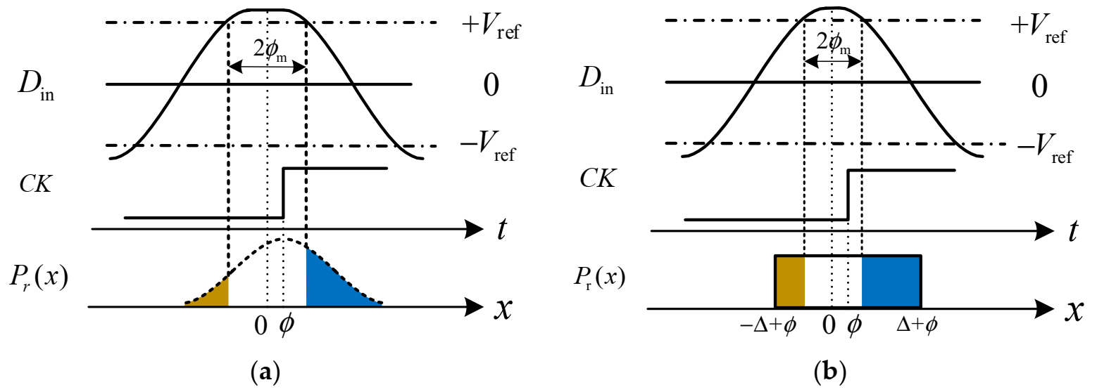
2.2. Linear Gain of MMPD

Just as it has been done to the BBPD in [7,8,14], the binary output characteristic of the MMPD is smoothed out by the jitter inherent in the input data and the recovery clock. First, we assume that the phase error (i.e., the phase difference between the input data and the recovery clock) consists of two terms: one is the deterministic phase error ue,U (e.g., deterministic ISI or sinusoidal jitter) and the other is the random phase error ue,G (e.g., Gaussian white noise) [9]. That is:
u = α × u e , G + β × u e , U .
where u is the average output of the MMPD, and α , β are the weights of the random phase error and the deterministic phase error, respectively.
When the phase error between the input data and the recovery clock is dominated by the random error term, we abstract the input jitter using a Gaussian probability density function with a standard deviation of σ and a mean value of 0.
Combining the operation of the MMPD in the clock and data recovery circuit, we assign “1” to phase “late” and “−1” to phase “early”, and then sum the positive and negative samples with weights given by the probabilities of their occurrence. Therefore, the average output of the MMPD is:
u = ( 1 ) P r ( l a t e | ϕ ) + ( 1 ) P r ( e a r l y | ϕ ) .
In Figure 3a, ϕ indicates the average phase difference between the input data and the recovery clock, 2 ϕ m is the drift bit width, namely the part of the input data whose voltage amplitude is greater than +Vref or less than −Vref. According to the Gaussian distribution probability density function, we obtain
P r ( l a t e | ϕ ) = 1 σ 2 π ϕ m exp ( ( x ϕ ) 2 2 σ 2 ) d x .
Let y = x ϕ 2 σ and f ( y ) = e y 2 1 y 2 , then
P r ( l a t e | ϕ ) 1 2 ( ϕ m ϕ 2 π σ ( ϕ m ϕ ) 3 6 2 π σ 3 ) .
Similarly, we can have
P r ( e a r l y | ϕ ) 1 2 ( ϕ m + ϕ 2 π σ ( ϕ m + ϕ ) 3 6 2 π σ 3 ) .
Substituting (4) and (5) into (2), we get
u e , G = ( 1 ) P r ( l a t e | ϕ ) + ( 1 ) P r ( e a r l y | ϕ ) 2 σ 2 ϕ m 2 2 π σ 3 ϕ .
When the phase error between the input data and the recovery clock is dominated by the deterministic error term, we abstract the input jitter using a uniform distribution probability density function with a standard deviation of σ and a mean value of 0. From Figure 3b, we get
P r ( l a t e | ϕ ) = ϕ m Δ + ϕ 1 2 Δ d x = Δ + ϕ ϕ m 2 Δ .
Since the variance of the uniform distribution can be expressed as
σ 2 = E [ x 2 ] ( E [ x ] ) 2 = Δ 2 3 .
Substituting (8) into (7), then
P r ( l a t e | ϕ ) = 3 σ ϕ m + ϕ 2 3 σ .
Similarly, we can attain
P r ( e a r l y | ϕ ) = 3 σ ϕ m ϕ 2 3 σ .
Substituting (9) and (10) into (2), we get
u e , U = ( 1 ) P r ( l a t e | ϕ ) + ( 1 ) P r ( e a r l y | ϕ ) 1 3 σ ϕ .
Note that the detection density of the input data is not considered in (6) and (11). If the detector density of the input data is λ , the gain of the MMPD based on Gaussian jitter or uniform jitter is λ u .
By analyzing these two extreme jitter distributions of the MMPD, we perform the linearization of the MMPD and give the gain range. If the CDR system has a clean channel, then Gaussian jitter will dominate the factor and the gain of the MMPD is (6); if deterministic jitter dominates the system, the gain of the MMPD is (11). It can also be seen from (6) and (11) that the gain of the MMPD is inversely proportional to the input jitter. The higher the jitter is, the lower the gain will be. This is the key consideration when we design the MM-CDR system, because in Section 3, we will find that the performance metrics of the CDR system will vary significantly as the jitter changes.
To verify the correctness of the MMPD linear gain model, we add the corresponding jitter to the sampler clock and then scan the phase difference at the input and count the number of overruns and lags to compute its average gain. Figure 4a,b show that the theoretical calculation agrees well with the simulation results. In addition, we find that for Gaussian jitter with a jitter variance of 0.1 UI and a drift bit width of 0.05 UI, the linear region of the MMPD is about ϕ   < 0.1   UI ; for uniform jitter with a jitter variance of 0.12 UI and a drift bit width of 0.05 UI, the linear region of the MMPD is about ϕ   < 0.15   UI . When we continue to increase the phase difference at the input, it can be observed that the MMPD will no longer have linear gain, but enter the nonlinear region, as illustrated in Figure 4c,d.

3. Small Signal Model of MM-CDR

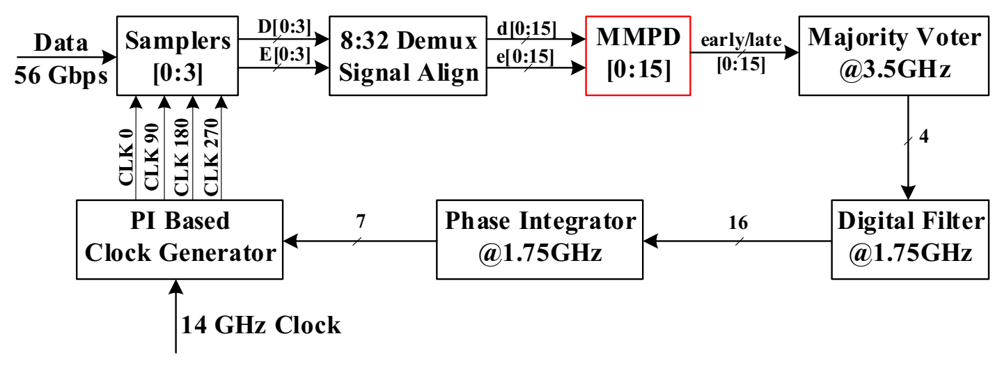
3.1. Linear Voting Model

Majority voting is implemented in CDR by adding the N-bit parallel PD output together and then taking the sign of results. Compared to the boxcar filter, voting is able to reduce the loop delay and lower the output noise of the MMPD. Hence, the digital CDR generally adopts voting as the decimation operation.
The gain of voting relies on the MMPD output and needs to be analyzed jointly with the MMPD. Taking a bank of four Mueller–Muller phase detectors via voting as an example, we give all the possible inputs leading to the output results in Table 2.
If the input jitter is Gaussian, the probability of the MMPD output 0, −1, 1 is determined when the phase difference is fixed. According to the principle of probability statistics, the probability when the voting output is “late” (i.e., 1) is
P v o t e ( l a t e ) = C 4 1 P 0 3 P l a + C 4 2 P 0 2 P l a 2 + C 4 2 C 2 1 P l a 2 P 0 P e a + C 4 1 P l a 3 P e a + C 4 1 P l a 3 P 0 + P l a 4 .
where P0, Pla, and Pea are the probabilities when the MMPD output are “no decision” (i.e., 0), “late” (i.e., 1), and “early” (i.e., −1) respectively.
P v o t e ( early ) = C 4 1 P 0 3 P e a + C 4 2 P e a 2 P 0 2 + C 4 2 C 2 1 P e a 2 P 0 P l a + C 4 1 P e a 3 P l a + C 4 1 P e a 3 P 0 + P e a 4 .
Finally, we obtain the united gain of the MMPD and the voting:
u = ( 1 ) P v o t e ( l a t e ) + ( 1 ) P v o t e ( e a r l y ) .
To compare the impact of the voter with Boxcar on the loop and get the gain of the voter, we simulate the joint gain of MMPD and Vote, as shown by the red line in Figure 5, whose gain can be expressed as K MD × K V . At the same time, we also simulate the joint gain of MMPD and boxcar filter, as depicted by the blue line in Figure 5, whose gain can be expressed as K MD × 1 . The gain ratio of these two cases can be obtained through simulation as well, and finally the gain of the voter can be derived. Figure 5a,b show that the MMPD-based voting is greatly affected by jitter and drift bit width, with the gain of the voter around 0.54 when the jitter is much larger than the drift bit width, and around 0.78 when the drift bit width is close to the jitter. Therefore, to perform analysis and fully understand the impact of voting, it is important to obtain accurate jitter and drift bit width.

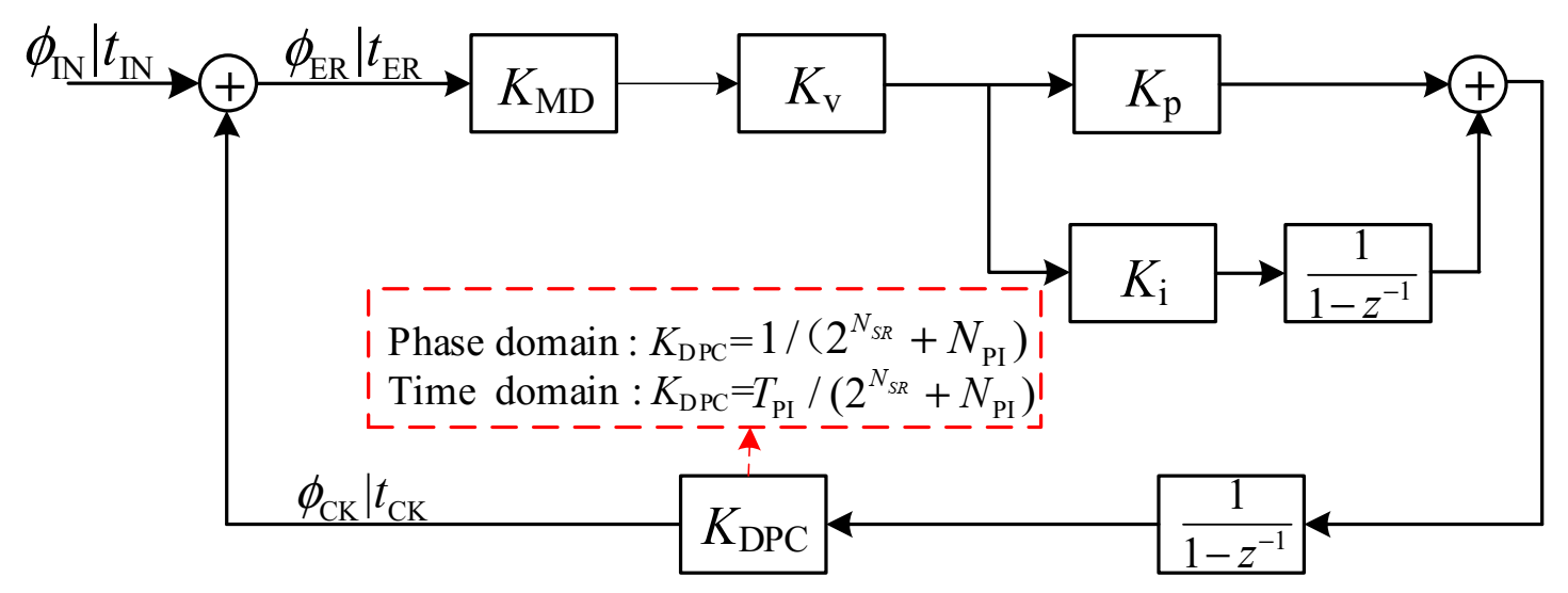
3.2. Linearized Analysis of CDR System

Based on the linear model of the MMPD in Section 2.2 and the analysis of the digital CDR in [8], we can obtain the small-signal model of the MM-CDR. In this section, according to the proposed architecture in Figure 6, we first present the linearized model (see Figure 7) and then analyze its transfer function and jitter tolerance.
Generally, the CDR must meet certain jitter performance specifications. Therefore, we first obtain the loop gain:
G ( z 1 ) = K MD K V K DP C 1 z 1 ( K p + K i 1 z 1 ) .
where KMD is the gain of MMPD; KV is the gain to handle the voting; the values of Ki and Kp correspond to the proportional and integral paths from the output of the voting to the digital-to-phase converter (DPC); the element KDPC is the gain through DPC. These parameters are listed above in Table 3.
Then, the transfer function of the MM-CDR can be calculated by the following well-known equation:
H JTRAN ( z ) = G ( z 1 ) / ( 1 + G ( z 1 ) )
The jitter tolerance is the maximum amount of input jitter that can be tolerated by the clock and data recovery circuit at a given bit error rate (BER) [15]. Therefore, the jitter tolerance computed by (17) for a target BER is 10−10.
H JTOL ( z ) = ( 1 12 σ ER T ) ( 1 + G ( z 1 ) ) .
where σ E R is the error jitter between recover clock and data, and T is the data cycle.
Figure 8 and Figure 9 plot the jitter transfer and jitter tolerance separately. It can be seen that as the jitter increases, the bandwidth of the MM-CDR decreases and the jitter tolerance becomes smaller.

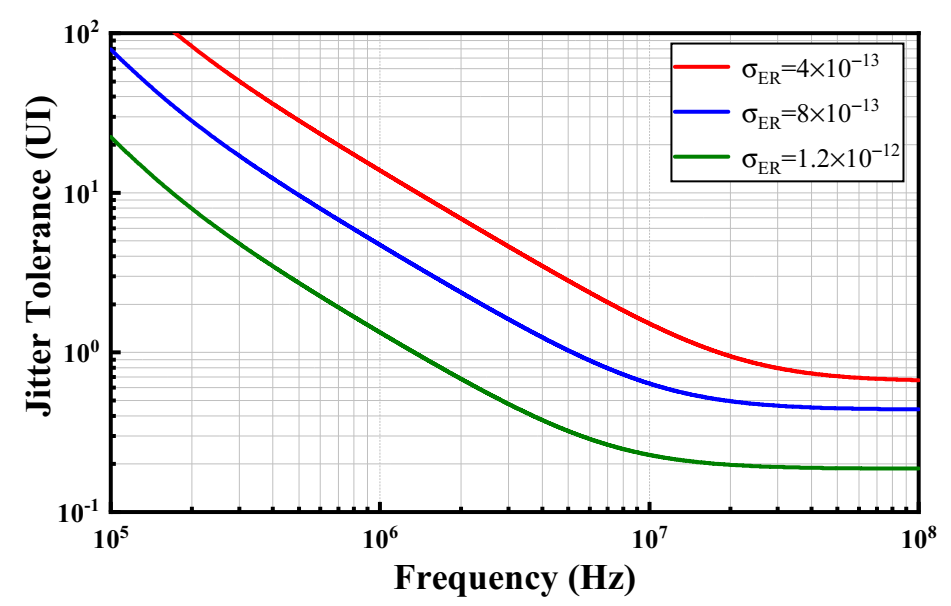
4. Jitter Analysis of MM-CDR

As discussed in Section 3.2 and [16], the MM-CDR loop characteristics vary with the error jitter σ ER . To obtain an accurate MM-CDR model, the exact error jitter is required. One possible way is to accurately simulate the entire system at one time, measure the error jitter, and then build a linear model. Nevertheless, this will greatly lengthen the design cycle. In contrast, if we estimate the error jitter in advance based on the circuit characteristics, we can not only obtain accurate CDR performance metrics, but also shorten the design cycle. Here, we focus on the effect of the two main sources of jitter on the error jitter: input data jitter and PI quantization noise [17].
In this work, we assume that there is a clean channel and the noise of the input data is generated by the oscillator at the transmitter. For simplicity, we only consider the main noise of the oscillator (i.e., thermal noise). Its noise power spectral density (PSD) as a function of the offset frequency f is given by [18],
S DAT = n f 2 ,
where n is the coefficient of the oscillator thermal noise. The period jitter of the input data σ DAT can be obtained by integrating the phase noise with the transfer function 1 z 1 [19].
σ DAT 2 = ( T 2 π ) 2 0 1 z 1 2 × S DAT d f n T 3 2 .
Substituting (19) into (18), the noise of input data can be written as
S DAT = 2 σ DAT 2 T 3 f 2 .
According to [20], in order to reduce the loop bandwidth and jitter peaking during design, we usually provide a larger damping factor ζ , so the transfer function can be approximated by that of a one-pole system. Using time instead of phase, the error transfer function is
t ER t IN = s s + w 3 dB   ( w 3 dB = K MD α , α = K V K p T PI 2 N S R N PI T DLF ) .
where w 3 dB is the bandwidth of MM-CDR; TPI is the period of phase interpolator’s input clock; TDLF is the period of digital filter. Combining (20) and (21), the error jitter contributed by the input data jitter is
σ ER , in 2 = T 2 4 π 2 0 2 σ DAT 2 T 3 f 2 s s + w 3 dB 2 d f = σ DAT 2 2 T w 3 dB .
According to Section 2.2, we indicate with σ ER , in the rms value of the jitter out of the MMPD, we can write:
K MD = λ 2 σ ER , in 2 ϕ m 2 2 π σ ER , in 3 .
Note that we consider the error jitter σ ER , in caused by the input data noise as the total error jitter, and in Section 5 we will give the reasonableness analysis. Combining (21)–(23), we have,
σ ER , in σ DAT 2 2 π + 2 π σ DAT 4 + 32 ϕ m 2 T 2 α 2 λ 2 8 T α λ .
Moreover, the quantization noise of PI is not negligible, and we consider that the PI oscillates between two phases. Assuming that the data phase has a delay of “x” with respect to the recovery clock, the phase of the recovery clock with respect to the previous moment when PI is rotated is = T PI / N PI , where is the minimum step of PI. Therefore, for random jitter, “x” is continuously varying, the average error jitter is
σ ER , PI 2 ( x ) = 1 Δ 0 Δ ( Δ x ) 2 + x 2 2 d x = Δ 2 3 .
In other words, the absolute jitter of the CDR due to quantization noise of the PI can be expressed as
σ ER , PI = T PI N PI 3 .
The total error jitter of the system is the combination of the values of each system RJ by the root mean square summing (RSS),
σ ER , tot = σ ER , in 2 + σ ER , PI 2 .
Which gives an estimate of the error jitter and will be verified in the simulation results in Section 5.

5. Results

The simulations in Figure 10 are obtained using a 56 Gb/s quarter-rate Mueller–Muller clock and data recovery circuit on 28 nm CMOS, with the structure shown in Figure 6.
We use a 56 GHz clock with period jitter to generate a PRBS31 code as the input data. Varying the input data jitters, the number of phases of the PI and sub-resolution of the phase integrator measure the error jitters between the recovered clock and the input data. The results are shown in Figure 10, where black dashed, green solid, and the red dashed lines correspond to (24), (26) and (27), respectively. The blue line with circles represents the error jitter of a CDR operating on 56 Gbps of serial data. Figure 10a–c respectively show the relationship between the results and the following factors: input data jitter, the number of phases of the PI, and sub-resolution of the phase integrator. it can be seen from Figure 10a that the error jitter caused by the input jitter is the dominant factor at this point, and when σ DAT increases, the total error jitter increases as well.
According to Figure 10b, the total error jitter follows the quantization noise of PI when NPI is low, and when NPI is high, σ ER , tot varies in accordance with σ ER , in . In fact, the MM-CDR bandwidth is large at low NPI, and (21) is high-pass, thus the input jitter has little effect on the total error jitter, and the quantization noise of PI accounts for the dominant factor. This has been validated by the simulation results in Figure 10b.
In Figure 10c, we can find that although the contribution of the input jitter to the total error jitter increases as NSR increases, it is still too small compared to the quantization noise of PI, and the fluctuation of σ ER , in does not cause the growth of the total error jitter. When σ ER , in is the dominant factor, the total error jitter approaches the error jitter caused by the input jitter, so the estimate using (23) is reasonable.

6. Conclusions

In this paper, we present a linear model of the MM-CDR. First, we design a model for the MMPD gain as in Equation (6) when Gaussian jitter is the dominant factor and Equation (11) when uniform jitter is the dominant one. In order to build a complete linear model, we introduce an estimation model for the error jitter, which achieves a sub-picosecond accuracy in the high-speed case. It is worth mentioning that the gain of the MMPD-based voter varies greatly with the error jitter and drift bit width, so it needs to be simulated accurately.

Author Contributions

Conceptualization, T.L. (Tao Liu) and T.L. (Tiejun Li); methodology, T.L. (Tao Liu); validation, T.L. (Tao Liu), M.W.; D.L.; formal analysis, T.L. (Tao Liu), F.L.; investigation, M.W., D.L.; resources, T.L. (Tiejun Li), H.W., B.L.; data curation, H.W.; writing—original draft preparation, T.L. (Tao Liu), F.Z.; writing—review and editing, T.L. (Tao Liu), X.Z., F.L.; supervision, B.L., T.L. (Tiejun Li), H.W., F.Z.; project administration, T.L. (Tiejun Li); funding acquisition, X.Z., F.L. All authors have read and agreed to the published version of the manuscript.

Funding

This research was funded by National Key R&D Program of China under Grant 2018YFB2202300.

Conflicts of Interest

The authors declare no conflict of interest.

References

  1. Shin, D.; Kim, H.S.; Liu, C.c.; Wali, P.; Murthy, S.K.; Fan, Y. A 23.9-to-29.4GHz Digital LC-PLL with a Coupled Frequency Doubler for Wireline Applications in 10 nm FinFET. In Proceedings of the 2021 IEEE International Solid-State Circuits Conference (ISSCC), San Francisco, CA, USA, 13–22 February 2021; pp. 188–190. [Google Scholar]
  2. Rahman, W.; Yoo, D.; Liang, J.; Sheikholeslami, A.; Tamura, H.; Shibasaki, T.; Yamaguchi, H. A 22.5-to-32-Gb/s 3.2-pJ/b Referenceless Baud-Rate Digital CDR with DFE and CTLE in 28-nm CMOS. IEEE J. Solid State Circuits 2017, 52, 3517–3531. [Google Scholar] [CrossRef]
  3. Ting, C.; Liang, J.; Sheikholeslami, A.; Kibune, M.; Tamura, H. A blind baud-rate ADC-based CDR. In Proceedings of the 2013 IEEE International Solid-State Circuits Conference. Digest of Technical Papers, San Francisco, CA, USA, 17–21 February 2013; pp. 122–123. [Google Scholar]
  4. Joy, A.K.; Mair, H.; Lee, H.; Feldman, A.; Portmann, C.; Bulman, N.; Crespo, E.C.; Hearne, P.; Huang, P.; Kerr, B.; et al. Analog-DFE-based 16Gb/s SerDes in 40nm CMOS that operates across 34dB loss channels at Nyquist with a baud rate CDR and 1.2Vpp voltage-mode driver. In Proceedings of the 2011 IEEE International Solid-State Circuits Conference, San Francisco, CA, USA, 20–24 February 2011; pp. 350–351. [Google Scholar]
  5. Harwood, M.; Warke, N.; Simpson, R.; Leslie, T.; Amerasekera, A.; Batty, S.; Colman, D.; Carr, E.; Gopinathan, V.; Hubbins, S.; et al. A 12.5Gb/s SerDes in 65nm CMOS Using a Baud-Rate ADC with Digital Receiver Equalization and Clock Recovery. In Proceedings of the 2007 IEEE International Solid-State Circuits Conference. Digest of Technical Papers, San Francisco, CA, USA, 11–15 February 2007; pp. 436–591. [Google Scholar]
  6. Francese, P.A.; Toifl, T.; Buchmann, P.; Brändli, M.; Menolfi, C.; Kossel, M.; Morf, T.; Kull, L.; Andersen, T.M. A 16 Gb/s 3.7 mW/Gb/s 8-Tap DFE Receiver and Baud-Rate CDR With 31 kppm Tracking Bandwidth. IEEE J. Solid State Circuits 2014, 49, 2490–2502. [Google Scholar] [CrossRef]
  7. Jri, L.; Kundert, K.S.; Razavi, B. Analysis and modeling of bang-bang clock and data recovery circuits. IEEE J. Solid State Circuits 2004, 39, 1571–1580. [Google Scholar] [CrossRef] [Green Version]
  8. Sonntag, J.L.; Stonick, J. A Digital Clock and Data Recovery Architecture for Multi-Gigabit/s Binary Links. IEEE J. Solid State Circuits 2006, 41, 1867–1875. [Google Scholar] [CrossRef]
  9. Park, M.; Kim, J. Pseudo-Linear Analysis of Bang-Bang Controlled Timing Circuits. IEEE Trans. Circuits Syst. I Regul. Pap. 2013, 60, 1381–1394. [Google Scholar] [CrossRef]
  10. Dokania, R.; Kern, A.; He, M.; Faust, A.; Tseng, R.; Weaver, S.; Yu, K.; Bil, C.; Liang, T.; Mahony, F.O. A 5.9pJ/b 10Gb/s serial link with unequalized MM-CDR in 14nm tri-gate CMOS. In Proceedings of the 2015 IEEE International Solid-State Circuits Conference—(ISSCC). Digest of Technical Papers, San Francisco, CA, USA, 22–26 February 2015; pp. 1–3. [Google Scholar]
  11. Choi, M.C.; Ko, H.G.; Oh, J.; Joo, H.Y.; Lee, K.; Jeong, D.K. A 0.1-pJ/b/dB 28-Gb/s Maximum-Eye Tracking, Weight-Adjusting MM CDR and Adaptive DFE with Single Shared Error Sampler. In Proceedings of the 2020 IEEE Symposium on VLSI Circuits, Honolulu, HI, USA, 16–19 June 2020; pp. 1–2. [Google Scholar]
  12. Spagna, F.; Chen, L.; Deshpande, M.; Fan, Y.; Gambetta, D.; Gowder, S.; Iyer, S.; Kumar, R.; Kwok, P.; Krishnamurthy, R.; et al. A 78mW 11.8Gb/s serial link transceiver with adaptive RX equalization and baud-rate CDR in 32nm CMOS. In Proceedings of the 2010 IEEE International Solid-State Circuits Conference—(ISSCC), San Francisco, CA, USA, 7–11 February 2010; pp. 366–367. [Google Scholar]
  13. Maity, S.; Mehrotra, P.; Sen, S. An Improved Update Rate Baud Rate CDR for Integrating Human Body Communication Receiver. In Proceedings of the 2018 IEEE Biomedical Circuits and Systems Conference (BioCAS), Cleveland, OH, USA, 17–19 October 2018; pp. 1–4. [Google Scholar]
  14. Ramezani, M.; Andre, C.; Salama, T. Jitter analysis of a PLL-based CDR with a bang-bang phase detector. In Proceedings of the the 2002 45th Midwest Symposium on Circuits and Systems, Tulsa, OK, USA, 4–7 August 2002; p. III. [Google Scholar]
  15. Talegaonkar, M.; Inti, R.; Hanumolu, P.K. Digital clock and data recovery circuit design: Challenges and tradeoffs. In Proceedings of the 2011 IEEE Custom Integrated Circuits Conference (CICC), San Jose, CA, USA, 19–21 September 2011; pp. 1–8. [Google Scholar]
  16. Liang, J.; Sheikholeslami, A.; Tamura, H.; Yamaguchi, H. On-Chip Jitter Measurement Using Jitter Injection in a 28 Gb/s PI-Based CDR. IEEE J. Solid State Circuits 2018, 53, 750–761. [Google Scholar] [CrossRef]
  17. Liang, J. Loop Gain Adaptation for Optimum Jitter Tolerance in Digital CDRs. IEEE J. Solid State Circuits 2018, 53, 2696–2708. [Google Scholar] [CrossRef]
  18. Behzad, R. Predicting the Phase Noise and Jitter of PLLBased Frequency Synthesizers. In Phase-Locking in High-Performance Systems: From Devices to Architectures; IEEE: New York, NY, USA, 2003; pp. 46–69. [Google Scholar]
  19. Azeredo-Leme, C. Clock Jitter Effects on Sampling: A Tutorial. IEEE Circuits Syst. Mag. 2011, 11, 26–37. [Google Scholar] [CrossRef]
  20. Razavi, B. Design of Integrated Circuits for Optical Communications; John Wiley & Sons: Hoboken, NJ, USA, 2012. [Google Scholar]
Figure 1. Mueller–Muller PD structure.
Electronics 10 01888 g001
Figure 2. MMPD phase detection waveform.
Electronics 10 01888 g002
Figure 3. Smoothing of PD characteristic due to jitter. (a) Gaussian jitter and (b) uniform jitter.
Electronics 10 01888 g003
Figure 4. Simulated gain of MMPD. (a) Gaussian jitter at small phase difference, (b) uniform jitter at small phase difference, (c) Gaussian jitter at large phase difference, and (d) uniform jitter at large phase difference.
Electronics 10 01888 g004
Figure 5. Simulated decimation by voting and boxcar, (a) σ = 0.1   UI ,     ϕ m = 0.05   UI , (b)   σ = 0.06   UI ,     ϕ m = 0.01   UI .
Electronics 10 01888 g005
Figure 6. The architecture of 56 Gb/s quarter-rate MMPD-based digital CDR.
Electronics 10 01888 g006
Figure 7. The linearized model of Figure 6.
Electronics 10 01888 g007
Figure 8. Jitter transfer of different input jitters.
Electronics 10 01888 g008
Figure 9. Jitter tolerance of different input jitters.
Electronics 10 01888 g009
Figure 10. Comparison of model and simulation results of the error jitter with various (a)   σ DAT , (b) NPI, and (c) NSR.
Electronics 10 01888 g010
Table 1. Truth table of MMPD.
D (n − 2)D (n − 1)D (n)E (n − 2)E (n − 1)E (n)Phase Info.
001x10LATE
00110xEARLY
011x01LATE
01101xEARLY
100x01LATE
10001xEARLY
110x10LATE
110100EARLY
OtherNo Info.
Table 2. Input and output of vote.
Voting OutputAll Circumstances
110001100110−1111−111101111
−1−1000−1−100−1−101−1−1−11−1−1−10−1−1−1−1
00000001−111−1−1
Note: All inputs in the table for the voting are in no particular order.
Table 3. MM-CDR parameter table.
ParameterValue
Gain of MMPD (KMD)16.0, 8.7, 5.9 per UI
Gain of vote (KV)0.58 × 32 = 19.2
Proportional path (KP)1
Integral path (Ki)2−13
Phase integrator’s sub-resolution (NSR)6
Number of phases of the PI (NPI)64
Publisher’s Note: MDPI stays neutral with regard to jurisdictional claims in published maps and institutional affiliations.

