Analysis and Modeling of Mueller–Muller Clock and Data Recovery Circuits
Abstract
:1. Introduction
2. Mueller–Muller Phase Detector
2.1. Working Principle of MMPD
2.2. Linear Gain of MMPD
3. Small Signal Model of MM-CDR
3.1. Linear Voting Model
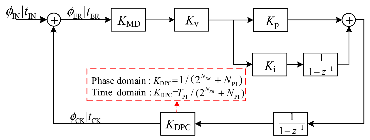
3.2. Linearized Analysis of CDR System
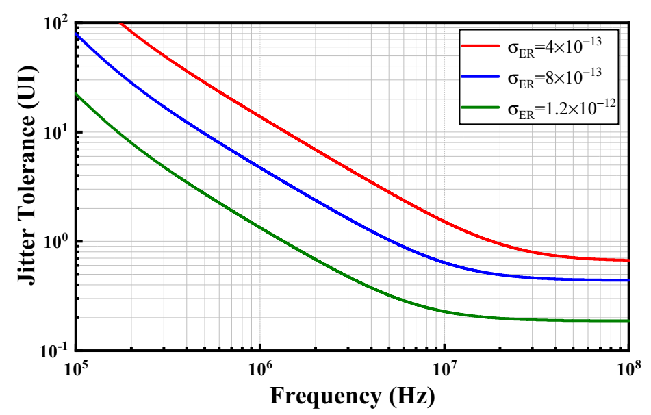
4. Jitter Analysis of MM-CDR
5. Results
6. Conclusions
Author Contributions
Funding
Conflicts of Interest
References
- Shin, D.; Kim, H.S.; Liu, C.c.; Wali, P.; Murthy, S.K.; Fan, Y. A 23.9-to-29.4GHz Digital LC-PLL with a Coupled Frequency Doubler for Wireline Applications in 10 nm FinFET. In Proceedings of the 2021 IEEE International Solid-State Circuits Conference (ISSCC), San Francisco, CA, USA, 13–22 February 2021; pp. 188–190. [Google Scholar]
- Rahman, W.; Yoo, D.; Liang, J.; Sheikholeslami, A.; Tamura, H.; Shibasaki, T.; Yamaguchi, H. A 22.5-to-32-Gb/s 3.2-pJ/b Referenceless Baud-Rate Digital CDR with DFE and CTLE in 28-nm CMOS. IEEE J. Solid State Circuits 2017, 52, 3517–3531. [Google Scholar] [CrossRef]
- Ting, C.; Liang, J.; Sheikholeslami, A.; Kibune, M.; Tamura, H. A blind baud-rate ADC-based CDR. In Proceedings of the 2013 IEEE International Solid-State Circuits Conference. Digest of Technical Papers, San Francisco, CA, USA, 17–21 February 2013; pp. 122–123. [Google Scholar]
- Joy, A.K.; Mair, H.; Lee, H.; Feldman, A.; Portmann, C.; Bulman, N.; Crespo, E.C.; Hearne, P.; Huang, P.; Kerr, B.; et al. Analog-DFE-based 16Gb/s SerDes in 40nm CMOS that operates across 34dB loss channels at Nyquist with a baud rate CDR and 1.2Vpp voltage-mode driver. In Proceedings of the 2011 IEEE International Solid-State Circuits Conference, San Francisco, CA, USA, 20–24 February 2011; pp. 350–351. [Google Scholar]
- Harwood, M.; Warke, N.; Simpson, R.; Leslie, T.; Amerasekera, A.; Batty, S.; Colman, D.; Carr, E.; Gopinathan, V.; Hubbins, S.; et al. A 12.5Gb/s SerDes in 65nm CMOS Using a Baud-Rate ADC with Digital Receiver Equalization and Clock Recovery. In Proceedings of the 2007 IEEE International Solid-State Circuits Conference. Digest of Technical Papers, San Francisco, CA, USA, 11–15 February 2007; pp. 436–591. [Google Scholar]
- Francese, P.A.; Toifl, T.; Buchmann, P.; Brändli, M.; Menolfi, C.; Kossel, M.; Morf, T.; Kull, L.; Andersen, T.M. A 16 Gb/s 3.7 mW/Gb/s 8-Tap DFE Receiver and Baud-Rate CDR With 31 kppm Tracking Bandwidth. IEEE J. Solid State Circuits 2014, 49, 2490–2502. [Google Scholar] [CrossRef]
- Jri, L.; Kundert, K.S.; Razavi, B. Analysis and modeling of bang-bang clock and data recovery circuits. IEEE J. Solid State Circuits 2004, 39, 1571–1580. [Google Scholar] [CrossRef] [Green Version]
- Sonntag, J.L.; Stonick, J. A Digital Clock and Data Recovery Architecture for Multi-Gigabit/s Binary Links. IEEE J. Solid State Circuits 2006, 41, 1867–1875. [Google Scholar] [CrossRef]
- Park, M.; Kim, J. Pseudo-Linear Analysis of Bang-Bang Controlled Timing Circuits. IEEE Trans. Circuits Syst. I Regul. Pap. 2013, 60, 1381–1394. [Google Scholar] [CrossRef]
- Dokania, R.; Kern, A.; He, M.; Faust, A.; Tseng, R.; Weaver, S.; Yu, K.; Bil, C.; Liang, T.; Mahony, F.O. A 5.9pJ/b 10Gb/s serial link with unequalized MM-CDR in 14nm tri-gate CMOS. In Proceedings of the 2015 IEEE International Solid-State Circuits Conference—(ISSCC). Digest of Technical Papers, San Francisco, CA, USA, 22–26 February 2015; pp. 1–3. [Google Scholar]
- Choi, M.C.; Ko, H.G.; Oh, J.; Joo, H.Y.; Lee, K.; Jeong, D.K. A 0.1-pJ/b/dB 28-Gb/s Maximum-Eye Tracking, Weight-Adjusting MM CDR and Adaptive DFE with Single Shared Error Sampler. In Proceedings of the 2020 IEEE Symposium on VLSI Circuits, Honolulu, HI, USA, 16–19 June 2020; pp. 1–2. [Google Scholar]
- Spagna, F.; Chen, L.; Deshpande, M.; Fan, Y.; Gambetta, D.; Gowder, S.; Iyer, S.; Kumar, R.; Kwok, P.; Krishnamurthy, R.; et al. A 78mW 11.8Gb/s serial link transceiver with adaptive RX equalization and baud-rate CDR in 32nm CMOS. In Proceedings of the 2010 IEEE International Solid-State Circuits Conference—(ISSCC), San Francisco, CA, USA, 7–11 February 2010; pp. 366–367. [Google Scholar]
- Maity, S.; Mehrotra, P.; Sen, S. An Improved Update Rate Baud Rate CDR for Integrating Human Body Communication Receiver. In Proceedings of the 2018 IEEE Biomedical Circuits and Systems Conference (BioCAS), Cleveland, OH, USA, 17–19 October 2018; pp. 1–4. [Google Scholar]
- Ramezani, M.; Andre, C.; Salama, T. Jitter analysis of a PLL-based CDR with a bang-bang phase detector. In Proceedings of the the 2002 45th Midwest Symposium on Circuits and Systems, Tulsa, OK, USA, 4–7 August 2002; p. III. [Google Scholar]
- Talegaonkar, M.; Inti, R.; Hanumolu, P.K. Digital clock and data recovery circuit design: Challenges and tradeoffs. In Proceedings of the 2011 IEEE Custom Integrated Circuits Conference (CICC), San Jose, CA, USA, 19–21 September 2011; pp. 1–8. [Google Scholar]
- Liang, J.; Sheikholeslami, A.; Tamura, H.; Yamaguchi, H. On-Chip Jitter Measurement Using Jitter Injection in a 28 Gb/s PI-Based CDR. IEEE J. Solid State Circuits 2018, 53, 750–761. [Google Scholar] [CrossRef]
- Liang, J. Loop Gain Adaptation for Optimum Jitter Tolerance in Digital CDRs. IEEE J. Solid State Circuits 2018, 53, 2696–2708. [Google Scholar] [CrossRef]
- Behzad, R. Predicting the Phase Noise and Jitter of PLLBased Frequency Synthesizers. In Phase-Locking in High-Performance Systems: From Devices to Architectures; IEEE: New York, NY, USA, 2003; pp. 46–69. [Google Scholar]
- Azeredo-Leme, C. Clock Jitter Effects on Sampling: A Tutorial. IEEE Circuits Syst. Mag. 2011, 11, 26–37. [Google Scholar] [CrossRef]
- Razavi, B. Design of Integrated Circuits for Optical Communications; John Wiley & Sons: Hoboken, NJ, USA, 2012. [Google Scholar]
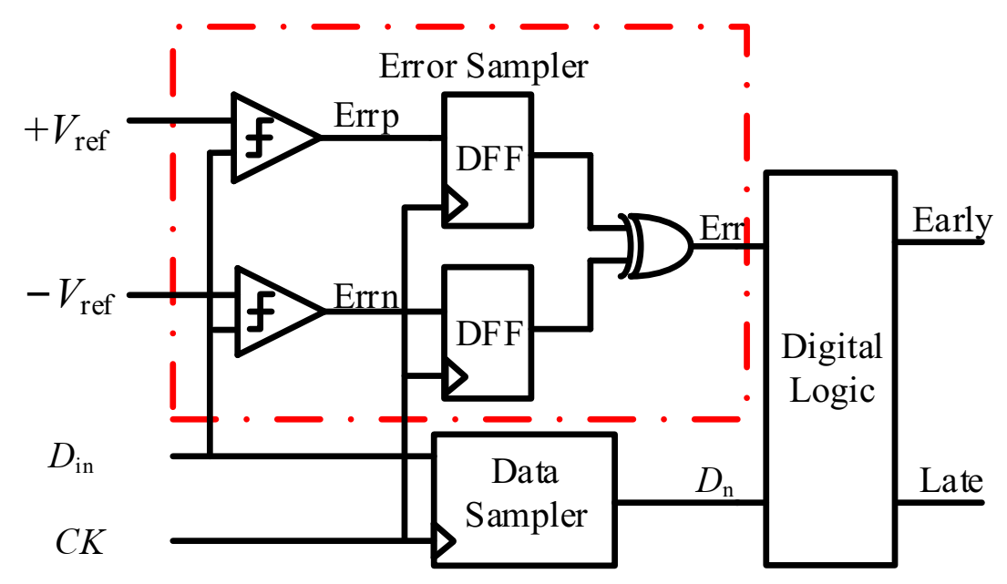
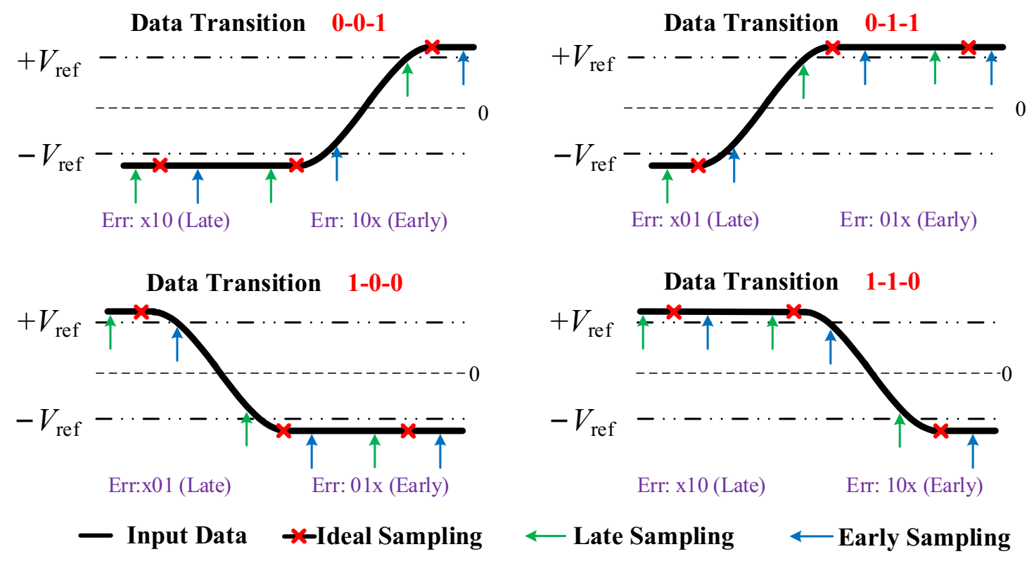
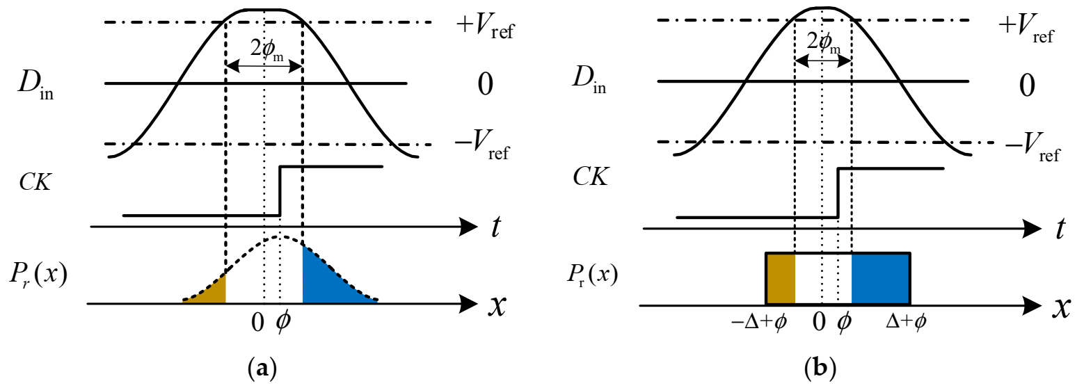


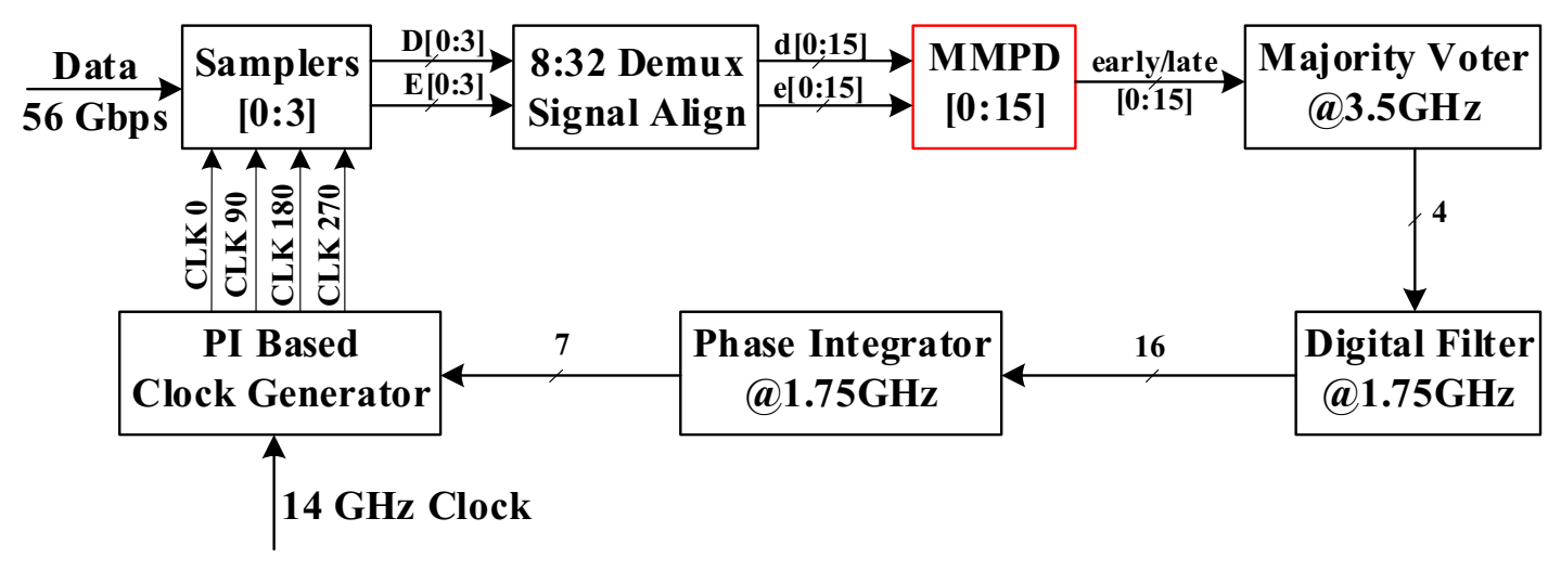


| D (n − 2) | D (n − 1) | D (n) | E (n − 2) | E (n − 1) | E (n) | Phase Info. |
|---|---|---|---|---|---|---|
| 0 | 0 | 1 | x | 1 | 0 | LATE |
| 0 | 0 | 1 | 1 | 0 | x | EARLY |
| 0 | 1 | 1 | x | 0 | 1 | LATE |
| 0 | 1 | 1 | 0 | 1 | x | EARLY |
| 1 | 0 | 0 | x | 0 | 1 | LATE |
| 1 | 0 | 0 | 0 | 1 | x | EARLY |
| 1 | 1 | 0 | x | 1 | 0 | LATE |
| 1 | 1 | 0 | 1 | 0 | 0 | EARLY |
| Other | No Info. | |||||
| Voting Output | All Circumstances | |||||
|---|---|---|---|---|---|---|
| 1 | 1000 | 1100 | 110−1 | 111−1 | 1110 | 1111 |
| −1 | −1000 | −1−100 | −1−101 | −1−1−11 | −1−1−10 | −1−1−1−1 |
| 0 | 0000 | 001−1 | 11−1−1 | |||
| Parameter | Value |
|---|---|
| Gain of MMPD (KMD) | 16.0, 8.7, 5.9 per UI |
| Gain of vote (KV) | 0.58 × 32 = 19.2 |
| Proportional path (KP) | 1 |
| Integral path (Ki) | 2−13 |
| Phase integrator’s sub-resolution (NSR) | 6 |
| Number of phases of the PI (NPI) | 64 |
Publisher’s Note: MDPI stays neutral with regard to jurisdictional claims in published maps and institutional affiliations. |
© 2021 by the authors. Licensee MDPI, Basel, Switzerland. This article is an open access article distributed under the terms and conditions of the Creative Commons Attribution (CC BY) license (https://creativecommons.org/licenses/by/4.0/).
Share and Cite
Liu, T.; Li, T.; Lv, F.; Liang, B.; Zheng, X.; Wang, H.; Wu, M.; Lu, D.; Zhao, F. Analysis and Modeling of Mueller–Muller Clock and Data Recovery Circuits. Electronics 2021, 10, 1888. https://doi.org/10.3390/electronics10161888
Liu T, Li T, Lv F, Liang B, Zheng X, Wang H, Wu M, Lu D, Zhao F. Analysis and Modeling of Mueller–Muller Clock and Data Recovery Circuits. Electronics. 2021; 10(16):1888. https://doi.org/10.3390/electronics10161888
Chicago/Turabian StyleLiu, Tao, Tiejun Li, Fangxu Lv, Bin Liang, Xuqiang Zheng, Heming Wang, Miaomiao Wu, Dechao Lu, and Feng Zhao. 2021. "Analysis and Modeling of Mueller–Muller Clock and Data Recovery Circuits" Electronics 10, no. 16: 1888. https://doi.org/10.3390/electronics10161888
APA StyleLiu, T., Li, T., Lv, F., Liang, B., Zheng, X., Wang, H., Wu, M., Lu, D., & Zhao, F. (2021). Analysis and Modeling of Mueller–Muller Clock and Data Recovery Circuits. Electronics, 10(16), 1888. https://doi.org/10.3390/electronics10161888


