Article

Taylor-Series-Based Reconfigurability of Gamma Correction in Hardware Designs

Department of Electronics Engineering, Dong-A University, Busan 49315, Korea
*
Author to whom correspondence should be addressed.
Electronics 2021, 10(16), 1959; https://doi.org/10.3390/electronics10161959
Submission received: 23 June 2021 / Revised: 10 August 2021 / Accepted: 11 August 2021 / Published: 14 August 2021
(This article belongs to the Special Issue Reconfigurable Digital Systems: Development and Applications)

Abstract

:
Gamma correction is a common image processing technique that is common in video or still image systems. However, this simple and efficient method is typically expressed using the power law, which gives rise to practical difficulties in designing a reconfigurable hardware implementation. For example, the conventional approach calculates all possible outputs for a pre-determined gamma value, and this information is hardwired into memory components. As a result, reconfigurability is unattainable after deployment. This study proposes using the Taylor series to approximate gamma correction to overcome the aforementioned challenging problem, hence, facilitating the post-deployment reconfigurability of the hardware implementation. In other words, the gamma value is freely adjustable, resulting in the high appropriateness for offloading gamma correction onto its dedicated hardware in system-on-a-chip applications. Finally, the proposed hardware implementation is verified on Zynq UltraScale+ MPSoC ZCU106 Evaluation Kit, and the results demonstrate its superiority against benchmark designs.

1. Introduction

Automation has garnered a keen interest from industrial and academic communities, as clearly witnessed by the rapid growth in autonomous driving vehicles and intelligent surveillance systems. Notably, machine vision algorithms play a crucial role in the progress towards full automation, and so do the constituent low-level image processing techniques. The reason is that visual data are more informative than other sensory data, showing greater potential for a successful amalgamation between humans and machines in workplaces. Concerning these low-level techniques, gamma correction (GC) is an essential part of the in-camera image processing pipeline in its well-known application in image encoding [1]. In this context, according to Stevens’s power law [2], the human visual system is more sensitive to differences between dark tones than between bright tones. Hence, GC allows allocating the number of bits to encode image intensities dynamically, that is, more bits for dark tones and fewer bits for bright tones. Consequently, this encoding scheme efficiently uses bits/bandwidth to store/transmit images.
Recently, GC has been exploited in image dehazing algorithms [3,4]. As an apparent corollary of Koschmieder’s law [5], the hazy image is brighter than the originally clean image due to the light scattered when light photons encounter microscopic aerosols in the atmosphere. Galdran [3] exploited this idea and demonstrated that selectively fusing several under-exposed versions of the hazy image could attain the dehazing effect. In this approach, GC was utilized to artificially under-expose the input image to create corresponding images for the subsequent image fusion. The reason for selecting GC was mainly its simplicity from the software perspective. Because GC is typically expressed using the power-law, it solely takes three floating-point operations to process a red–green–blue (RGB) image. Moreover, the exponentiation by the squaring algorithm of C’s standard library facilitates the fast implementation of GC. However, from the hardware perspective, GC is relatively cumbersome. As a common practice, hardware designers realize GC by means of look-up tables (LUTs), which have been hardwired using pairs of pre-calculated input–output data. For example, Ngo et al. [4] improved the method of Galdran [3] and proposed an efficient hardware architecture in which GC was realized as LUTs. However, the LUT-based realization of GC limits the performance tuning of this dehazing system because the gamma parameter in GC is fixed for determining the content of LUTs. As a result, users have to tune other parts of the system rather than the GC, even though GC directly influences the dehazing performance. Therefore, run-time reconfigurability of GC is still unattainable.
As discussed thus far, a conspicuous disadvantage of LUT-based GC design lies in the inability to freely adjust the gamma parameter because of the pre-calculation of LUTs’ content. This study, hence, proposes a run-time reconfigurable implementation of GC using the Taylor series. More specifically, the power form of GC is first modified to include the exponential and logarithmic functions. Then, the fourth Taylor polynomial of the exponential function is used to approximate the original power form. This polynomial also serves as the floating-point description for the hardware design phase. Next, the error tolerance of ± 1 least significant bit (LSB) is selected to derive the corresponding fixed-point description, which serves as a blueprint for the hardware implementation. Although the floating-point description can be used to derive the hardware design directly, this type of implementation requires a substantial amount of hardware resources. Therefore, the conversion to the fixed-point format, which reduces the number of bits representing the design’s internal signals, is a necessary step. Finally, Zynq UltraScale+ MPSoC ZCU106 Evaluation Kit (Xilinx Asia Pacific Pte. Ltd., Singapore, Singapore) is used to validate the real-time processing capability.
The rest of this paper is organized as follows. Section 2 presents background knowledge about GC and Taylor series. Section 3 reviews the major implementation platforms, while Section 4 briefly explores existing hardware architectures for realizing GC. After that, Section 5 details the proposed hardware implementation, including the floating-point design and the hardware described by Verilog hardware description language (IEEE Standard 1364-2005) [6]. Section 5 also provides the implementation results and demonstrates the real-time processing capability, while Section 6 describes the hardware verification using Zynq UltraScale+ MPSoC ZCU106 Evaluation Kit (Xilinx Asia Pacific Pte. Ltd., Singapore, Singapore). Finally, Section 7 concludes the paper.

2. Preliminaries

This section briefly introduces the GC and Taylor series, serving as a hinge point for the subsequent description of the proposed method in Section 5.

2.1. Gamma Correction in Image Processing

Once, at the dawn of television technology, GC was invented to nullify the display’s nonlinear input–output characteristic. For example, in the early cathode ray tube display, the beam intensity is nonlinearly proportional to the voltage applied to the electron gun. Accordingly, applying GC to the input signal can cancel out this nonlinearity [7]. However, GC not only compensates the display device’s characteristic; it is also appropriate to the encoding paradigm for optimizing image storage/transmission, as mentioned earlier in Section 1. Thus, this interesting combination of coincidence and engineering facilitates early television technology.
Mathematically, GC is typically expressed using the power law, in which the non-negative real-valued input intensity Y i n is raised to the power γ to obtain the output intensity Y o u t . In the image processing field, input and output data are generally normalized to the range between zero and unity, and the power (henceforth referred to as gamma parameter or gamma value) is positive. Figure 1 depicts three modes of GC, corresponding to γ < 1 , γ = 1 , and γ > 1 . For γ < 1 , specifically, γ = 0.5 in Figure 1a, dark details become easily noticeable at the cost of bright detail loss. Conversely, bright details are of better clarity, whereas dark details may be black-limited, as illustrated in Figure 1c for γ > 1 ( γ = 2 ). Finally, when γ = 1 , as depicted in Figure 1b, the input data is left unchanged.
Y o u t = Y i n γ .
Regarding the recent use of GC in image dehazing, the third operation mode corresponding to γ > 1 is referred to as artificial image under-exposure. In this context, the gamma value denotes the under-exposure degree, and it is inversely proportional to the image brightness. Because the hazy image exhibits a substantial increase in luminance, applying GC with different gamma values is analogous to restoring the actual luminance of hazy constituent regions. Consequently, judiciously fusing these regions from under-exposed images can produce a satisfactory result with desirable dehazing effects. As discussed previously, Galdran [3] and Ngo et al. [4] approached image dehazing from this perspective, and their results were of comparative quality compared with other state-of-the-art dehazing algorithms. Notwithstanding such an on-par performance, the processing time was impressively fast due to the simplicity of pixel-wise operations, such as GC and image fusion. The discussion thus far has demonstrated that the simple and efficient GC is of fundamental importance in the image processing field.

2.2. Taylor Series

The Taylor series of a function—named after Brook Taylor [8]—is an infinite sum of its derivatives at a single point, as shown in Equation (2). The notation T { f ( x ) } denotes the Taylor series of a real-valued function f ( x ) , which must be infinitely differentiable at a real number a. The right-hand side of Equation (2) is also called the nth Taylor polynomial, where n takes on non-negative integer values, n ! denotes the factorial of n, and f ( n ) ( a ) denotes the nth derivative of the function f ( x ) evaluated at the point x = a . It is noteworthy that the partial sums of the series are widely used to approximate the function. The approximation’s accuracy increases as more terms are included.
T { f ( x ) } = n = 0 f ( n ) ( a ) n ! ( x a ) n .
In mathematics, the Fourier series is similar to the Taylor series to a certain extent because it also expresses a periodic function as an infinite sum of sines and cosines. However, this study selects the Taylor series for function approximation for two main reasons. Firstly, the Taylor series calculation only requires the knowledge of the function on the proximity of a point. In contrast, calculating the Fourier series requires that the function is defined on a whole domain interval. Accordingly, using the Taylor series results in a considerably small error in the point proximity where it is computed. Furthermore, the powers in the Taylor series’s partial sums are much easier to realize in the hardware implementation phase than the sines and cosines of the Fourier series.
The exponential function e x p ( x ) and its corresponding Taylor series at the origin ( a = 0 ), shown in Equation (3), are prime examples of function approximation using the Taylor series. As illustrated in Figure 2, all five Taylor polynomials considered therein are precisely equal to the exponential function at the point a = 0 . However, approximation errors increase at points farther away from the origin, and they are inversely proportional to the polynomial degree n. When n = 0 , the Taylor polynomial is simply one, and this polynomial is the least favorable approximation. When n becomes larger, the Taylor polynomial better resembles the actual exponential function—depicted as the solid blue line in Figure 2. Nevertheless, a too-large value of n places a heavy burden on the hardware implementation phase. Fortunately, it can be deduced from Figure 2 that the fourth Taylor polynomial is virtually identical to the exponential function in a small neighborhood around the point a = 0 . Hence, this study utilizes the fourth Taylor polynomial to approximate the exponential function.
T { e x p ( x ) } = n = 0 x n n ! .

3. A Brief Review of Implementation Platforms

Currently, the central processing unit (CPU), graphics processing unit (GPU), and field-programmable gate array (FPGA) are prevailing implementation platforms. Among them, the CPU and GPU offer distinct advantages in terms of flexibility, portability, and programming abstraction, which are beneficial to algorithm development and verification. Despite the convenience that CPUs and GPUs offer, achieving high computing performance and energy efficiency is not easy. More specifically, by their nature, CPUs are general-purpose platforms and thus have to sacrifice computing performance and energy efficiency for flexibility and portability. Meanwhile, GPUs offer a higher level of parallelism than CPUs; hence, they typically consume more energy to ensure high computing performance. In contrast, due to their high-speed processing capability, reconfigurability, and energy efficiency, FPGAs offer an attractive alternative option, albeit with a burden of development and verification.
Concerning the processing speed per se, GPUs stand out as a potential candidate because they can handle image data quickly while not requiring considerable development effort. In practice, they are the primary platform for training and running deep neural networks. For example, Zhang and Tao [9] presented a dehazing network that could handle 620 × 460 images at 35 frames per s (fps) with an Nvidia Titan Xp. Nevertheless, in real-world embedded systems, processing speed is often considered together with energy efficiency. Accordingly, GPUs appear to be less efficient owing to high power consumption and short lifespan, leading to the gradually increasing preference of FPGAs to GPUs [10]. However, owing to the potential exhaustion of computing resources, FPGAs cannot completely substitute GPUs when implementing deep neural networks whose inherent computational complexity is exceptionally high. Instead, FPGA-GPU heterogeneity is a feasible and efficient stopgap [11]. A prime example is that Microsoft Research leveraged FPGAs to accelerate its Bing search engine, resulting in a 50 % increase in throughput of the search ranking [12]. Except for implementing deep neural networks, FPGAs typically outperform GPUs in terms of processing speed and energy efficiency when implementing common image processing techniques, as demonstrated by various studies in the literature [13,14,15,16]. In the previous example of image dehazing, an FPGA realization of a similar algorithm can process 4096 × 2160 (4K) images at 30.7 fps [17]. Therefore, FPGA-based implementations are highly appropriate for real-world embedded systems, where processing speed and energy consumption are critical.
Notably, low-power GPUs do exist for integrating into real-world embedded systems. The Tegra X2 GPU equipped on the Nvidia Jetson TX2 board is a prime example. According to a thorough investigation by Wielage et al. [18], Tegra X2 GPU was more efficient than the contemporary Xilinx Virtex UltraScale+ FPGA under power consumption per se. However, when considering power consumption in conjunction with processing speed, Xilinx Virtex UltraScale+ FPGA was 6.5× times faster than Tegra X2 GPU, while the power efficiency was 4.3 × times lower. Those findings suggest that low-power GPUs are possible alternatives to FPGAs when the power and performance budgets can be sacrificed to shorten the time to market. In contrast, FPGAs are the best choice to achieve low power consumption and high computing performance in real-world embedded systems.

4. Related Work

In general, hardware designers implement GC using either LUTs [19,20] or piece-wise linear polynomial approximation [21,22,23]. The LUT-based realization is seemingly the most straightforward method, in which input–output pairs for a specific gamma value are hardwired into memories. As discussed earlier in Section 1, this method fixes the gamma parameter at a particular value, which significantly reduces the flexibility. As a result, hardware designers have to resort to using several LUTs for different gamma values if they aim to increase flexibility. For example, a typical eight-bit input, eight-bit output LUT requires 2048 bits for one gamma value. If the GC design supports 128 different gamma values, the total memory requirement is 32 KB. This amount of memory may be problematic for resource-constrained platforms—such as microprocessors (μPs) and microcontrollers (μCs)—because GC is a simple operation that cannot occupy too much space in the system memory. In addition, realizing GC using LUTs is also subject to banding artifacts. As illustrated in Figure 3a, the GC’s curve possesses a steeper slope at low input values than high input values. Accordingly, the large jumps in the output values may cause banding artifacts. Hardware designers often decrease the quantization step by using more bits to represent the input data to solve this problem, thus increasing the LUT’s size and incurring a heavy memory burden.
Observing the limitations of the LUT-based method, hardware designers have proposed an alternative that employs piece-wise linear polynomial approximation. Under this approach, the input domain is divided into segments that are not necessarily equal in size. Then, for each segment, the corresponding output values are calculated using linear approximation or interpolation, as illustrated in Figure 3b. Although this approach alleviates the memory burden, the precision of output data is lower than that of the LUT-based approach. The method proposed by Lee et al. [23] improved the precision by employing hierarchical segmentation to partition the input domain in a nonuniform manner. Their method ensured that the resulting segments were minimal, and the accuracy was ± 1 LSB. Nevertheless, methods using piece-wise linear polynomial approximation do not support adjusting the gamma parameter freely. Similarly to LUT-based methods, they also require pre-determining the gamma parameter to calculate corresponding polynomial coefficients in each segment. The lack of on-the-fly tuning ability limits the breadth of GC’s applications in real-world systems.
Because the development of memory and transistor technologies is currently not as fast as it used to be, it is difficult to increase the processing speed of the CPU and GPU. Accordingly, heterogeneous computing platforms are becoming a viable alternative for high-performance computing. They typically include CPUs, GPUs, and FPGAs; hence, the communication between these constituents is essential to gain performance and energy efficiency. Consequently, the aforementioned lack of tuning ability is a serious obstacle for CPUs and GPUs to offload computations onto the GC’s accelerator. Therefore, this observation is the motivation for the Taylor-series-based implementation of GC in this study.

5. Proposed Method

This section describes the proposed method from a software perspective (floating-point description) to a hardware perspective (fixed-point description). It also discusses several aspects of the hardware design phase, which are exploitable to achieve a high processing speed.

5.1. Floating-Point Description

As a starting point, the power-law expressing GC in Equation (1) can be re-written in terms of exponential and logarithmic functions, as follows.
Y o u t = Y i n γ = e x p l n Y i n γ = e x p γ · l n Y i n ,
where e x p ( · ) and l n ( · ) denote the exponential and natural logarithmic functions, respectively. As described in Section 2.2, the exponential function can be accurately approximated by the fourth Taylor polynomial at the proximity around the origin. Therefore, the GC’s approximation can be obtained by letting A = γ · l n Y i n and then performing a neat conversion, based on the power to a power rule described in Equation (5), to ensure that the exponent is extremely small.
Y o u t = e x p ( A ) = e x p A 2 m 2 m 1 + B + B 2 2 + B 3 6 + B 4 24 2 m ,
where B = A / 2 m becomes extremely small for a fairly large value of m. More specifically, the larger the variable m is, the closer the exponent B is pushed to the origin. Consequently, the approximation using the Taylor polynomial in Equation (3) is more accurate. However, from the hardware designer’s perspective, a higher accuracy comes at the cost of increasing hardware resource utilization. Therefore, this study empirically sets m to ten ( m = 10 ) to balance this trade-off. Additionally, Equation (5) is slightly re-arranged to facilitate the subsequent hardware implementation, resulting in the floating-point description in Equation (6).
Y o u t 1 + B + B 2 2 + B 3 6 + B 4 24 2 m = 1 + B 1 + B 2 + B 2 6 1 + B 4 2 m .
Figure 4 provides a first and rough insight into the hardware utilization of the GC’s approximation based on the floating-point description. Because the logarithmic operation drops down the exponent γ , the problem that hinders the reconfigurability of GC is remedied. The computation of l n Y i n is attainable by pre-calculating all input–output pairs and storing the results in the on-chip memory (RAM). This type of implementation is reconfigurable because the memory contents can be updated at the run-time. Concerning the remaining operations, adders and multipliers suffice for a fast and compact implementation. At first glance, the GC’s approximation in Figure 4 requires a small RAM, four adders, and fifteen multipliers, which is relatively small compared with common operations such as division and square-root.
As mentioned earlier in Section 1, the floating-point description per se suffices for the hardware implementation. This type of hardware design is typically synthesized using C-like languages, such as C2Verilog [24] and Handle-C [25], and the time to market can be shortened significantly. Nevertheless, these high-level languages share two common problems pertinent to concurrency and timing control, as pointed out by Edwards [26]. As a result, Verilog (IEEE Standard 1364-2005) [6] and VHDL (IEEE Standard 1076-2019) [27] are still the main means for realizing signal processing algorithms in reconfigurable devices. Additionally, researchers and practitioners often leverage pipelined architectures and fixed-point representation to gain maximum benefits from Verilog and VHDL hardware description languages. The former refers to a set of processing elements that are connected in series and executed in parallel. This type of data processing scheme optimizes the throughput and thus improves processing speed [28]. Meanwhile, the latter refers to a particular technique for representing fractional values using binary numbers. This representation style reduces resource utilization and results in a compact hardware design. This study will describe these two relevant techniques in the following subsections.

5.2. Fixed-Point Description

The fixed-point description refers to a particular step in the hardware implementation phase, where each signal within the design is represented by a fixed number of bits (henceforth referred to as the signal’s word length interchangeably). The objective is to minimize the signal’s word length while retaining an acceptable accuracy compared with the floating-point description.
Fixed-point number representation is useful for representing fractional numbers in low-cost embedded μPs and μCs, where floating-point processing units are excluded to ensure low power consumption and low market price. Although fixed-point numbers are actually integer numbers, a “virtual” binary point is used to implicitly scale the numbers by a specific factor. For example, the binary number 01100011 2 represents the decimal value 143 10 . By adding a virtual binary point in the middle 0110 . 0011 2 , the represented decimal value becomes 6 . 1875 10 , as illustrated in Figure 5. The numbers of bits to the left and the right of the virtual point are called integer bits and fractional bits, respectively. For representing fixed-point numbers with corresponding word length, several notations have been developed. This study adopts the < s , p , i > notation of the LabVIEW programming language [29]. In this format, s serves as an indicator signifying whether the number is unsigned or 2’s complement signed. Accordingly, it is either + or ±, respectively. The remaining p denotes the word length, with i being the integer part. Following this notation, the fixed-point number in Figure 5 can be expressed as < + , 8 , 4 >.
The conversion from a real-valued floating-point number X to its corresponding fixed-point value X f i is shown in Equation (7). The · notation denotes the floor function (or round toward minus infinity), the subtraction ( p i ) denotes the number of fractional bits, and s g n ( · ) denotes the sign function–defined in Equation (8). In the definition of Equation (7), the round operation implicitly rounds the value X · 2 p i away from zero to the nearest integer with a larger magnitude, conforming with MATLAB R2019a’s definition. This type of rounding allows using MATLAB R2019a for fixed-point conversion, shortening the design time significantly.
X f i = X · 2 p i + s g n ( X ) · 1 2 ,
s g n ( X ) = { 1 X < 0 0 X = 0 1 X > 1
The goal of fixed-point design is to determine the word length of all signals in the design so that the output error remains within a pre-determined tolerance. In general, this error tolerance is ± 1 LSB for eight-bit image data. However, this study places the virtual point ahead of those eight bits to represent the normalization of image data. Accordingly, the bit position to calculate the error tolerance is at the eighth bit of the output. Given the error tolerance, the range of γ is another requisite for evaluating the output error. As discussed in Section 2.1, γ takes on positive real values that can theoretically increase to infinity. However, when γ becomes too large, most image data appear too dark to be discernible. In addition, a large number of bits is also required to represent the image data in that case, but current display devices are unable to support such image data. Consequently, this study empirically sets γ ’s word length to < + , 8 , 4 > , signifying that γ ranges from zero to 15 . 9375 10 at a step of 0 . 0625 10 . Figure 6 demonstrates the output error for all γ values, and it is easily noticeable that the error varies within the tolerance of ± 1 LSB. The detailed information about the word length of internal signals is illustrated in the data path in Figure 7. This data path serves as a blueprint for designing the hardware implementation.
In Figure 7, the input data are Y i n and γ with the corresponding word lengths of < + , 8 , 0 > and < + , 8 , 4 >, while the output data is represented by Y o u t , whose word length is < + , 25 , 0 >. Control signals include the clock, reset, horizontal active video, and vertical active video. They are used to ensure the synchronous operation and are denoted as Clock, Reset, hav, and vav in the bottom-left corner of Figure 7. At the beginning of the data path, two multiplexers are employed to discard the zero values of Y i n and γ because l n ( 0 ) is undefined and Y i n 0 is meaningless. After that, the data flow is analogous to that depicted in Figure 4, except that addition, multiplication, division, and square operations are now realized by digital circuits. Notably, although the split multiplier is functionally identical to the multiplier, it is pipelined to ensure a high throughput when multiplying numbers with large word lengths.

5.3. Hardware Implementation

Given the fixed-point description in the form of the data path in Figure 7, Verilog hardware description language is used to describe the hardware implementation. Because most of the operations are simple, this section solely focuses on the reconfiguration of the logarithmic function, which is realized by RAM, and the split multiplier, which pipelines the multiplication to achieve real-time processing.
Figure 8 depicts the block diagram of the hardware verification, whose top-left portion is the RAM’s content updating scheme. It is noteworthy that the RAM-based implementation of the logarithmic function enables run-time reconfigurability; that is, the RAM’s content can be updated dynamically. However, before describing how to update the RAM’s content in more detail, it is necessary to look quickly at the hardware verification. In Figure 8, the host computer is the master, which executes the “C platform” to provide the graphical user interface (GUI). Through the GUI, the “C platform” captures user-defined parameters and input data–including the RAM’s content and image data. It then writes that body of data to the DDR4 memory via the universal serial bus (USB) communication. As a result, the quad-core ARM® Cortex™-A53 processor on the Zynq UltraScale+ MPSoC ZCU106 Evaluation Kit (Xilinx Asia Pacific Pte. Ltd., Singapore, Singapore) (the slave in this hardware verification) can fetch the data. The “controller”, in turn, interacts with the ARM® Cortex™-A53 processor to obtain user-defined parameters and input data from DDR4 memory. At this time, the “controller” writes the RAM’s content to the on-chip RAM while also writing the image data to the read buffer memories located in the “double buffering interface”. After that, the “user design”, which contains the proposed run-time reconfigurable GC, retrieves the results of the logarithmic function from the on-chip RAM and processes the image data. Finally, the processed data are written back to the write buffer memories in the “double buffering interface” before the “controller” writes them to DDR4 memory. Therefore, the “C platform” can obtain the processed data via USB communication to display to the user.
Concerning the RAM’s content updating scheme, the “controller” uses the retrieved RAM’s content from DDR4 memory as “write data”. Meanwhile, it leverages a counter to generate the “write address” and enables the “write enable”. It then routes the “write address” to the address port of the on-chip RAM via the “select” signal. Most importantly, the “controller” utilizes the vertical active video signal to ensure that the write operation occurs during the vertical blank period—the time between the end of a frame and the beginning of the next frame—to avoid data corruption. For the read operation, the “controller” now disables the “write enable”, while the “logic circuits” uses the image data as the “read address”. The “controller” then routes the “read address” to the address port of the on-chip RAM via the “select” signal. Therefore, the “logic circuits” can retrieve the requisite results of the logarithmic function for processing the image data. Hence, this RAM’s content updating scheme, coupled with the Taylor-series-based approximation of the exponential function, results in the full reconfigurability of the proposed design at the run-time.
Another aspect to consider is the real-time processing capability. As depicted in Figure 7, timing violation is highly likely to occur in multipliers owing to the large word length of operands. In this study, the multiplication is pipelined, as depicted in Figure 9. Firstly, the M-bit multiplicand and N-bit multiplier are arbitrarily split into halves. The distributive and associative laws are then applied to break the original multiplication into four smaller parts. This process is demonstrated in Equation (9), where Q, A, and B denote the product, multiplicand, and multiplier, respectively. The multiplicand is separated into M 2 -bit A 2 and ( M M 2 ) -bit A 1 parts in that equation, and so is the multiplier whose two parts are N 2 -bit B 2 and ( N N 2 ) -bit B 1 . The derived addition operations (for example, A 1 B 1 2 M 2 + A 2 B 1 ) are then performed judiciously so that the hardware synthesis tool does not infer unnecessarily large adders. In the previous example, A 1 B 1 2 M 2 is equal to A 1 B 1 padded with M 2 zeros to the rear. Therefore, the corresponding M 2 LSBs of A 2 B 1 can be wired directly to the register containing the sum. It is only necessary to add the remaining bits of A 2 B 1 to A 1 B 1 and store the result in the corresponding location in the sum register.
Q = A · B = ( A 1 2 M 2 + A 2 ) · ( B 1 2 N 2 + B 2 ) = A 1 B 1 2 M 2 + N 2 + A 1 B 2 2 M 2 + A 2 B 1 2 N 2 + A 2 B 2 = ( A 1 B 1 2 M 2 + A 2 B 1 ) 2 N 2 + ( A 1 B 2 2 M 2 + A 2 B 2 )
In practice, real-time systems in real-world applications typically handle RGB image data. Therefore, this paper first presents two “user design” architectures—illustrated in Figure 10—to seek out the most efficient design that facilitates the integration into existing real-time systems. After that, it presents a comparative evaluation that assesses this chosen design against two conventional approaches discussed in Section 4. In Figure 10a, the proposed run-time reconfigurable GC is applied to the red, green, and blue image channels separately; hence, this design is named RGB-GC. By contrast, the architecture in Figure 10b first converts the input image to the YCbCr color space and then applies GC to the luminance channel only; therein lies the name YCbCr-GC. This architecture also leverages the chrominance subsampling [30] to convert the standard 4:4:4 YCbCr data into 4:2:2 format, reducing the hardware resource utilization for chrominance processing/storage. At first glance, the YCbCr-GC appears to be more compact and efficient than the RGB-GC. However, a detailed discussion on this issue will be presented at the end of this section to avoid rambling.

5.4. Implementation Results

The implementation results are summarized in Table 1, where slice registers, LUTs, and RAM36X1Ss are referred to as primitives—the simplest design elements in the Xilinx libraries. More precisely, slice registers and LUTs denote the logic area, while RAM36X1Ss denote the memory area. These quantities represent the area that the design will occupy on the target device. As demonstrated in Table 1, the two designs in Figure 10 are relatively compact and fast, as witnessed by a small hardware utilization and high operating frequency. More specifically, the RGB-GC utilizes, respectively, 1.09 % , 11.18 % , and 0.48 % of slice registers, LUTs, and RAM36X1Ss, while the corresponding percentages of the YCbCr-GC are 0.58 % , 4.29 % , and 0.16 % . Moreover, the fractional numbers of RAM36X1Ss utilized in the two design are worth an explanation. RAM36X1S is a 36 KB block RAM that can be configured as a total 36 KB RAM or two 18 KB RAMs [31]. In the proposed run-time reconfigurable GC, the RAM’s content is the pre-calculated values of l n Y i n —which have a word length of 14 bits; thus, it requires 0.4375 KB. Consequently, the RAM-based implementation of l n Y i n is mapped to an 18 KB RAM of RAM36X1S. In other words, it occupies half of RAM36X1S or 0.5 RAM36X1Ss. Therefore, the RGB-GC instantiates three GCs for red, green, and blue channels; hence, it utilizes 1.5 RAM36X1Ss. In contrast, the YCbCr-GC utilizes 0.5 RAM36X1Ss because it only instantiates one GC for the luminance channel. So, from the implementation results, it can be concluded that the YCbCr-GC is faster and more compact than the RGB-GC. It is also observed that the YCbCr-GC consumes less power than the RGB-GC, as demonstrated by the worst-case power consumption—which is a sum of static and dynamic power reported by Xilinx Vivado v2019.1 for worst-case operating conditions.
Furthermore, the maximum processing speeds (MPSs)—calculated using Equation (10) and tabulated in Table 2—demonstrate that these two designs can, respectively, process DCI 4K video at 34.35 and 35.21 fps. These results satisfy the real-time processing requirement of 30 fps for both PAL and NTSC color encoding systems [32]. In Equation (10), f m a x denotes the maximum operating frequency, ( H , W ) denotes the image’s height and width, and ( V B , H B ) denotes the vertical and horizontal blanks. It is worth noting that Xilinx Vivado v2019.1 does not provide the maximum operating frequency in the implementation report. Instead, this information was derived from the target clock period (T) and worst negative slack ( W N S ), as shown in Equation (11). In this study, both hardware designs can operate properly with ( V B , H B ) of at least one image line and one image pixel. Thus, the implementation results presented herein demonstrate that those two designs are highly appropriate for high-speed and high-quality image processing applications, both in standalone operation and in cooperation with other systems.
M P S = f m a x ( W + H B ) · ( H + V B ) ,
f m a x = 1 T W N S .
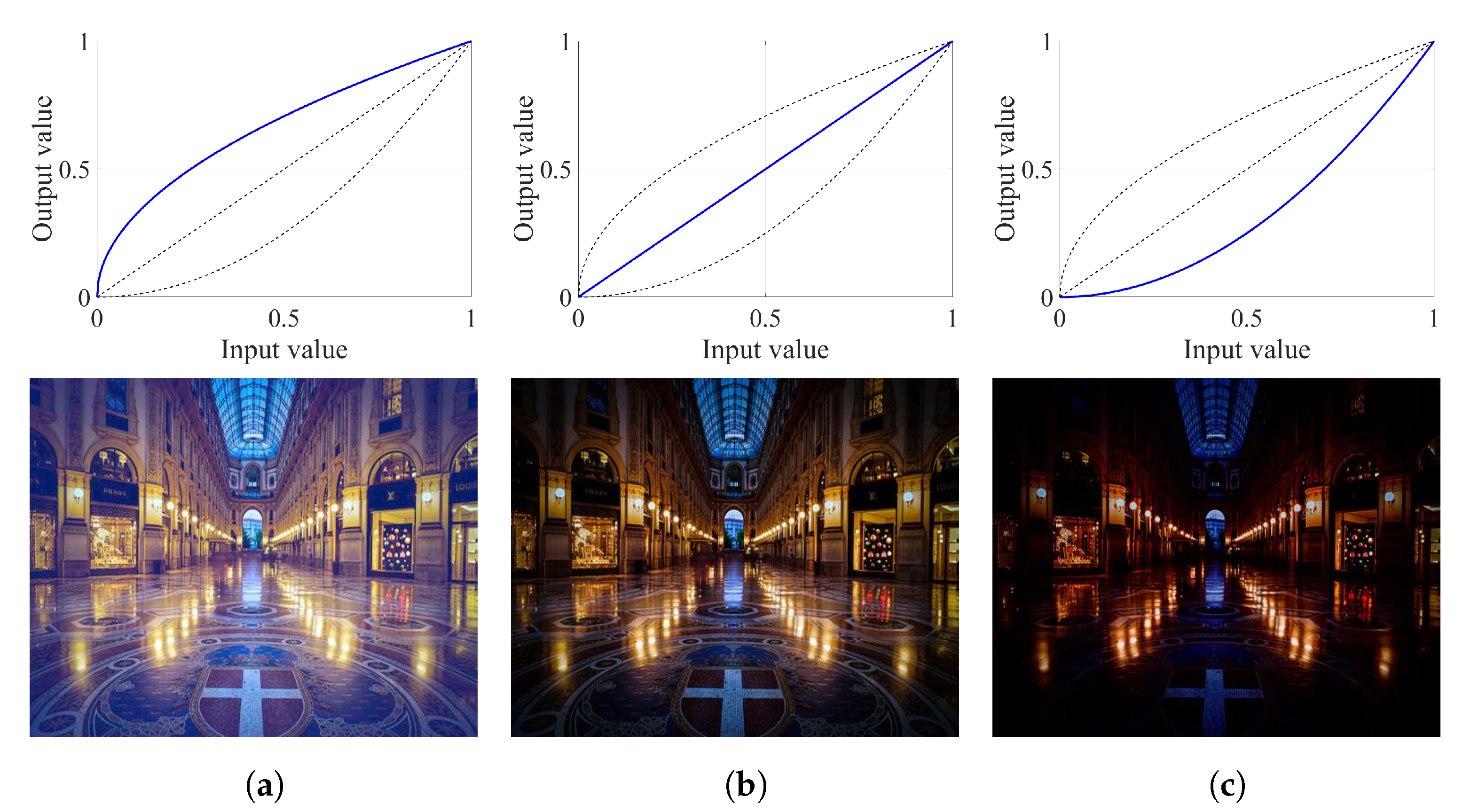
Figure 11 demonstrates a qualitative comparison between these two designs and the reference floating-point versions. As illustrated in Figure 11, the results of RGB-GC and YCbCr-GC are slightly different. However, this difference is insignificant because the γ parameter can be freely adjusted using the proposed architecture. Therefore, users can fine-tune the γ parameter to obtain the desired results. In addition, the hardware implementations are designed based on the fixed-point descriptions, which in turn are derived from the floating-point references with the error tolerance of ± 1 LSB. Hence, the difference between the results of RGB-GC and YCbCr-GC and their corresponding floating-point references (denoted as RGB-GC ref. and YCbCr-ref.) is indiscernible. This qualitative comparison, coupled with the implementation results, demonstrates the efficacy of the YCbCr-GC design.
Finally, the YCbCr-GC is compared against two conventional designs of GC—which employ LUTs and piecewise linear polynomial approximation. Table 3 summarizes the implementation results of these three designs in two cases where the gamma parameter is fixed and freely adjustable. The designs that employ LUTs and piecewise linear polynomial approximation are denoted as LUT-based GC and PLPA-based GC, respectively. In addition, because Lee et al. [23] provided the implementation results of these two benchmark designs in case the gamma parameter was fixed, this study reuses those data. In case the gamma parameter is freely adjustable, this study employs the reported data by Lee et al. [23] to calculate the corresponding memory utilization. In this case, for a fair comparison, the adjustable range of the gamma parameter is from zero to 15 . 9375 10 at a step of 0 . 0625 10 . As the gamma value of zero does not require any calculation, this range includes 255 different gamma values. Therefore, the LUT-based GC must be equipped with additional 255 LUTs to support adjusting the gamma parameter. Meanwhile, Lee et al. [23] have to add another 255 polynomial coefficient tables to their PLPA-based GC. Hence, these two designs suffer from a heavy memory burden as they require approximately 1 MB and 25 KB. By contrast, the proposed YCbCr-GC can handle both cases without any additional modifications.
A correction step is necessary for slice utilization because the YCbCr-GC and two benchmark designs are implemented on two different FPGA devices. Lee et al. [23] implemented the LUT-based and PLPA-based GC on a Xilinx Virtex-4 XC4VLX100-12 device, whereas this paper presents the implementation results of the YCbCr-GC for the Xilinx UltraScale XCZU7EV-2FFVC1156 device. According to the data sheets [33,34], a slice of the former device consists of eight LUTs and eight registers, while a slice of the latter device comprises eight LUTs and sixteen registers. As a result, 2686 slice registers and 9887 slice LUTs in Table 1 are converted into 1236 slices in Table 3. For two benchmark designs, they require a great number of LUTs and registers to handle the case where the gamma parameter is freely adjustable. Those added resources are primarily for routing the internal data according to the gamma parameter. However, because it is impossible to calculate the exact numbers without re-implementing benchmark designs by hand, Table 3 represents them as not available (NA). Therefore, in case the gamma parameter is fixed, the PLPA-based GC is the best design. Conversely, in case the gamma parameter is freely adjustable, the proposed YCbCr-GC is the most efficient. Additionally, because fixing the gamma parameter severely limits the practicality, it can be concluded that the proposed YCbCr-GC is superior to the two benchmark designs.

6. Verification

As briefly discussed in Section 5.3, a “C platform” running on a host computer is designed to monitor the operation of the “user design” implemented on Zynq UltraScale+ MPSoC ZCU106 Evaluation Kit (Xilinx Asia Pacific Pte. Ltd., Singapore, Singapore). Figure 12 depicts the platform and the board in the real-world execution. The platform consists of three main panels, in which the top panel displays the input–output data side-by-side for performance demonstration. The bottom-left panel comprises buttons for selecting the input data source and is called the platform control. Similarly, the bottom-right panel consists of buttons and slide bars for configuring the “user design” and is called the algorithm control. Thus, this platform provides a visual and convenient means to verify the real-time operation.
The algorithm control comprises a slide bar for adjusting the γ parameter and a click button for supplying the RAM’s content. The “C platform” captures those input data and transfers them to the Zynq UltraScale+ MPSoC ZCU106 Evaluation Kit (Xilinx Asia Pacific Pte. Ltd., Singapore, Singapore) via USB communication. In Figure 12, γ = 2 was used to produce the output image, and the “user design” implemented on the evaluation board was the YCbCr-GC. Although the output image in Figure 12 is identical to the corresponding result in Figure 11, a slight difference is noticeable. The reason is that Figure 12 was captured using the smartphone’s camera; hence, it is virtually impossible to account for all relevant factors such as imaging angle, monitor’s display characteristics, and lighting condition.
This verification demonstrates the practicality of the proposed run-time reconfigurable GC. Because the YCbCr-GC can handle RGB image data at a high processing rate, real-time image processing systems in autonomous driving vehicles or smart surveillance cameras can conveniently integrate it to attain high computing performance. In contrast, two benchmark designs presented by Lee et al. [23] are only able to handle single-channel image data. Therefore, it is burdensome to integrate them into existing real-time systems. Moreover, their lack of ability to tune the gamma parameter is still the biggest obstacle to their practicality.

7. Conclusions

This paper described a run-time reconfigurable hardware implementation of GC, an essential low-level image processing technique with various applications. As opposed to the conventional approaches, which fix the gamma parameter for hardware implementation, this study supported a freely adjustable gamma parameter by first re-organizing the power form of GC into the exponential function of the logarithm. It then exploited the fourth Taylor polynomial to obtain an accurate approximation. This approximation served as the floating-point description to perform the fixed-point design with the error tolerance of ± 1 LSB, resulting in a compact hardware implementation. Additional techniques, such as RAM-based logarithm implementation and pipelined multiplication, were also applied to attain the real-time processing capability, which was verified using Zynq UltraScale+ MPSoC ZCU106 Evaluation Kit (Xilinx Asia Pacific Pte. Ltd., Singapore, Singapore). According to the verification result, the proposed hardware design is highly appropriate for high-speed and high-quality image-processing applications.

Author Contributions

Conceptualization, B.K.; software, D.N.; validation, D.N.; data curation, D.N.; writing—original draft preparation, D.N.; writing—review and editing, B.K. and D.N.; visualization, D.N.; supervision, B.K. Both authors have read and agreed to the published version of the manuscript.

Funding

This research was supported by research funds from Dong-A University, Busan, Korea, grant number 20210623.

Conflicts of Interest

The authors declare no conflict of interest.

References

  1. Parulski, K.; Spaulding, K. Color image processing for digital cameras. In Digital Color Imaging Handbook; CRC Press: Boca Raton, FL, USA, 2003; Chapter 12; pp. 734–739. [Google Scholar]
  2. Stevens, S.S. On the psychophysical law. Psychol. Rev. 1957, 64, 153–181. [Google Scholar] [CrossRef] [PubMed]
  3. Galdran, A. Image dehazing by artificial multiple-exposure image fusion. Signal Process. 2018, 149, 135–147. [Google Scholar] [CrossRef]
  4. Ngo, D.; Lee, S.; Nguyen, Q.H.; Ngo, T.M.; Lee, G.D.; Kang, B. Single Image Haze Removal from Image Enhancement Perspective for Real-Time Vision-Based Systems. Sensors 2020, 20, 5170. [Google Scholar] [CrossRef] [PubMed]
  5. Lee, Z.; Shang, S. Visibility: How Applicable is the Century-Old Koschmieder Model? J. Atmos. Sci. 2016, 73, 4573–4581. [Google Scholar] [CrossRef]
  6. IEEE Std 1364-2005. IEEE Standard for Verilog Hardware Description Language; Revision of IEEE Std 1374-2001; IEEE: New York, NY, USA, 2006; pp. 1–590. [Google Scholar] [CrossRef]
  7. Charles, P. Digital Video and HD: Algorithms and Interfaces, 1st ed.; The Morgan Kaufmann Series in Computer Graphics; Morgan Kaufmann Publisher, Inc.: San Francisco, CA, USA, 2003. [Google Scholar]
  8. Struik, D.J. A Source Book in Mathematics, 1200–1800; Princeton Legacy Library, Princeton University Press: Princeton, NJ, USA, 2016. [Google Scholar]
  9. Zhang, J.; Tao, D. FAMED-Net: A Fast and Accurate Multi-Scale End-to-End Dehazing Network. IEEE Trans. Image Process. 2019, 29, 72–84. [Google Scholar] [CrossRef] [PubMed] [Green Version]
  10. Intel. FPGA vs. GPU for Deep Learning. Available online: https://www.intel.com/content/www/us/en/artificial-intelligence/programmable/fpga-gpu.html (accessed on 14 July 2021).
  11. Carballo-Hernandez, W.; Pelcat, M.; Berry, F. Why is FPGA-GPU Heterogeneity the Best Option for Embedded Deep Neural Networks? arXiv 2021, arXiv:2102.01343. [Google Scholar]
  12. Microsoft. Project Catapult. Available online: https://www.microsoft.com/en-us/research/project/project-catapult/ (accessed on 14 July 2021).
  13. Qasaimeh, M.; Denolf, K.; Lo, J.; Vissers, K.; Zambreno, J.; Jones, P. Comparing Energy Efficiency of CPU, GPU and FPGA Implementations for Vision Kernels. In Proceedings of the 2019 IEEE International Conference on Embedded Software and Systems (ICESS), Las Vegas, NV, USA, 2–3 June 2019; pp. 1–8. [Google Scholar] [CrossRef] [Green Version]
  14. Brugger, C.; Dal’Aqua, L.; Varela, J.A.; De Schryver, C.; Sadri, M.; Wehn, N.; Klein, M.; Siegrist, M. A quantitative cross-architecture study of morphological image processing on CPUs, GPUs, and FPGAs. In Proceedings of the 2015 IEEE Symposium on Computer Applications & Industrial Electronics (ISCAIE), Langkawi, Malaysia, 12–14 April 2015; pp. 201–206. [Google Scholar] [CrossRef]
  15. Fowers, J.; Brown, G.; Cooke, P.; Stitt, G. A performance and energy comparison of FPGAs, GPUs, and multicores for sliding-window applications. In Proceedings of the ACM/SIGDA International Symposium on Field Programmable Gate Arrays, Monterey, CA, USA, 22–24 February 2012; pp. 47–56. [Google Scholar] [CrossRef] [Green Version]
  16. Che, S.; Li, J.; Sheaffer, J.; Skadron, K.; Lach, J. Accelerating Compute-Intensive Applications with GPUs and FPGAs. In Proceedings of the 2008 Symposium on Application Specific Processors, Anaheim, CA, USA, 8–9 June 2008; pp. 101–107. [Google Scholar] [CrossRef]
  17. Ngo, D.; Lee, S.; Lee, G.D.; Kang, B. Single-Image Visibility Restoration: A Machine Learning Approach and Its 4K-Capable Hardware Accelerator. Sensors 2020, 20, 5795. [Google Scholar] [CrossRef] [PubMed]
  18. Wielage, M.; Cholewa, F.; Fahnemann, C.; Pirsch, P.; Blume, H. High Performance and Low Power Architectures: GPU vs. FPGA for Fast Factorized Backprojection. In Proceedings of the 2017 Fifth International Symposium on Computing and Networking (CANDAR), Aomori, Japan, 19–22 November 2017; pp. 351–357. [Google Scholar] [CrossRef]
  19. Akeley, K. Reality Engine graphics. In Proceedings of the 20th Annual Conference on Computer Graphics and Interactive Techniques, Anaheim, CA, USA, 2–6 August 1993; pp. 109–116. [Google Scholar] [CrossRef]
  20. Lucas, B. Method and Apparatus for Converting Floating-Point Pixel Values to Byte Pixel Values by Table Lookup. European Patent 0578950A2, 19 January 1994. [Google Scholar]
  21. Lin, T.P.; Cheng, H.M.; Kung, C.P. Adaptive Piece-Wise Approximation Method for Gamma Correction. U.S. Patent 6292165B1, 18 September 2001. [Google Scholar]
  22. Kim, E.S.; Jang, S.W.; Lee, S.H.; Jung, T.Y.; Sohng, K.I. Optimal Piece Linear Segments of Gamma Correction for CMOS Image Sensors. IEICE Trans. Electron. 2005, E88-C, 2090–2093. [Google Scholar] [CrossRef] [Green Version]
  23. Lee, D.U.; Cheung, R.; Villasenor, J. A Flexible Architecture for Precise Gamma Correction. IEEE Trans. Very Large Scale Integr. (VLSI) Syst. 2007, 15, 474–478. [Google Scholar] [CrossRef] [Green Version]
  24. Soderman, D.; Panchul, Y. Implementing C algorithms in reconfigurable hardware using C2Verilog. In Proceedings of the IEEE Symposium on FPGAs for Custom Computing Machines (Cat. No.98TB100251), Napa Valley, CA, USA, 17 April 1998; pp. 339–342. [Google Scholar] [CrossRef]
  25. Celoxica. Handel-C Language Reference Manual. Available online: https://celoxica.com/ (accessed on 14 April 2021).
  26. Edwards, S.A. The challenges of hardware synthesis from C-like languages. In Proceedings of the Design, Automation and Test in Europe, Munich, Germany, 7–11 March 2005; Volume 1, pp. 66–67. [Google Scholar] [CrossRef] [Green Version]
  27. IEEE Std 1076-2019. IEEE Standard for VHDL Language Reference Manual; IEEE: New York, NY, USA, 2019; pp. 1–673. [Google Scholar] [CrossRef]
  28. Patterson, D.; Hennessy, J. Computer Organization and Design MIPS Edition: The Hardware/Software Interface, 6th ed.; The Morgan Kaufmann Series in Computer Architecture and Design; Morgan Kaufmann Publisher, Inc.: San Francisco, CA, USA, 2020. [Google Scholar]
  29. Intruments, N. Fixed-Point (FXP) to Single (SGL) Conversion: LabVIEW 2011 FPGA Module and Earlier. Available online: https://www.ni.com/ko-kr/support/documentation/supplemental/21/fixed-point-fxp-to-single-sgl-conversion-labview-2011-fpga-module-and-earlier.html (accessed on 19 March 2021).
  30. Christian, J. Vision Models and Applications to Image and Video Processing. In Vision and Video: Models and Applications; Springer: New York, NY, USA, 2001; Chapter 10; pp. 208–209. [Google Scholar]
  31. Xilinx. Zynq UltraScale+ MPSoC Data Sheet: Overview. Available online: https://www.xilinx.com/support/documentation/data_sheets/ds891-zynq-ultrascale-plus-overview.pdf (accessed on 19 May 2021).
  32. Jack, K. NTSC and PAL Digital Encoding and Decoding. In Video Demystified, 4th ed.; Newnes: London, UK, 2005; Chapter 9; pp. 394–471. [Google Scholar]
  33. Xilinx. Virtex-4 FPGA User Guide. Available online: https://www.xilinx.com/support/documentation/user_guides/ug070.pdf (accessed on 15 July 2021).
  34. Xilinx. UltraScale Architecture Configurable Logic Block. Available online: https://www.xilinx.com/support/documentation/user_guides/ug574-ultrascale-clb.pdf (accessed on 15 July 2021).
Figure 1. Gamma correction curves and corresponding effects on an image: (a) γ = 0.5, (b) γ = 1, and (c) γ = 2.
Electronics 10 01959 g001
Figure 2. Exponential function and its Taylor series at zero.
Electronics 10 01959 g002
Figure 3. Illustrations of two implementation methods using (a) look-up table and (b) piece-wise linear polynomial approximation. A gamma value of 0.5 is assumed.
Electronics 10 01959 g003
Figure 4. Computational flow of the floating-point description.
Electronics 10 01959 g004
Figure 5. Example of fixed-point number representation.
Electronics 10 01959 g005
Figure 6. Error at the output for different γ values.
Electronics 10 01959 g006
Figure 7. Data path of the run-time reconfigurable gamma correction with explicit word length information. Clock, reset, hav, and vav denote the clock, reset, horizontal active video, and vertical active video signals.
Electronics 10 01959 g007
Figure 8. Block diagram of the hardware verification. The top-left portion is the RAM’s content updating scheme for run-time reconfigurability.
Electronics 10 01959 g008
Figure 9. Block diagram of split multiplier for real-time processing.
Electronics 10 01959 g009
Figure 10. Two hardware designs for facilitating the integration of the proposed run-time reconfigurable gamma correction into existing real-time systems: (a) the first design that processes the red–green–blue image data separately (RGB-GC), and (b) the second design that performs color space conversion and processes the luminance (YCbCr-GC).
Electronics 10 01959 g010
Figure 11. Qualitative comparison of the RGB-GC, YCbCr-GC, and their corresponding floating-point references.
Electronics 10 01959 g011
Figure 12. Real-world execution of the proposed run-time reconfigurable gamma correction.
Electronics 10 01959 g012
Table 1. Implementation results of the proposed run-time reconfigurable gamma correction designs. The symbol # denotes quantities.
Xilinx Vivado v2019.1 1
Device XCZU7EV-2FFVC1156
Slice Logic UtilizationAvailableRGB-GCYCbCr-GC
Used Utilization Used Utilization
Slice Registers (#)460,80050441.09%26860.58%
Slice LUTs (#)230,40025,75611.18%98874.29%
RAM36X1Ss (#)3121.50.48%0.50.16%
Worst-Case Power Consumption 2.562 W1.246 W
Minimum Period 3.288 ns3.208 ns
Maximum Frequency 304.136 MHz311.721 MHz
1 The EDA Tool was supported by the IC Design Education Center (IDEC).
Table 2. Maximum processing speeds for different video resolutions. The symbol # denotes quantities.
Video ResolutionFrame SizeRequired Clock Cycles (#)Processing Speed ( MPS )
RGB-GCYCbCr-GC
Full HD (FHD) 1920 × 1080 2,076,601146.46150.11
Quad HD (QHD) 2560 × 1440 3,690,40182.4184.47
4KUW4K 3840 × 1600 6,149,44149.4650.69
UHD TV 3840 × 2160 8,300,40136.6437.55
DCI 4K 4096 × 2160 8,853,61734.3535.21
Table 3. Comparative evaluation with two conventional approaches. NA stands for not available. The symbol # denotes quantities.
Gamma ParameterDesignMemory (KB)Slice (#)Worst-Case Power Consumption (W)
FixedLUT-based GC41035NA
PLPA-based GC0.0967177NA
YCbCr-GC0.437512361.246
Freely AdjustableLUT-based GC1020NANA
PLPA-based GC24.6585NANA
YCbCr-GC0.437512361.246
Publisher’s Note: MDPI stays neutral with regard to jurisdictional claims in published maps and institutional affiliations.

