Article

High-Linearity Direct Conversion Receiver with the Transconductance Equalization Technique and DCOC Method

Institute of Astronautic Electronic Engineering, School of Aeronautics and Astronautics, Zhejiang University, Hangzhou 310007, China
*
Author to whom correspondence should be addressed.
Electronics 2021, 10(16), 1966; https://doi.org/10.3390/electronics10161966
Submission received: 30 June 2021 / Revised: 10 August 2021 / Accepted: 12 August 2021 / Published: 15 August 2021
(This article belongs to the Section Circuit and Signal Processing)

Abstract

:
To improve the linearity of direct conversion receivers (DCRs), two high-linearity methods for high second-order intercept points (IP2s) and high third-order intercept points (IP3s) are proposed. To improve IP3s, a transconductance equalization technique for a complementary input operational amplifier (OPAMP) is proposed in an active-RC low-pass filter (LPF), while a digital-analog hybrid DC offset calibration (DCOC) method is proposed to improve IP2s. For one thing, the proposed transconductance equalization technique employs a pair of resistors to guarantee high voltage gain for an OPAMP with two-stage Miller topology under a high-input voltage swing to improve linearity with little deterioration of the noise performance. For another, during the DCOC method, the low-noise amplifier is turned off and replaced by an equivalent resistance of the output impedance of the low-noise amplifier to ensure the accuracy and effectiveness of the DCOC method. Fabricated in 40-nm CMOS technology, the receiver with proposed methods can realize a noise figure of 2.6–3.5 dB in the full frequency band, with an OIP3 of 28 dBm, an IM2 more than 70 dBc, and a remaining DC of −53.2 dBm under the total voltage gain of 60 dB.

1. Introduction

The direct conversion receiver (DCR) has the advantages of high integration, strong reconfigurability, and low cost, making it a preferred architecture for most radio frequency receivers [1]. In a high linearity design, improving the second-order intercept point (IP2) and the third-order intercept point (IP3) is a critical requirement of the DCR and the overall system.
First of all, for a high IP3, an RC-active filter is the preferred topology when achieving high linearity is the most critical design metric, because RC-active filters can realize high linearity and be capable of supporting a large voltage swing based on an operational amplifier (OPAMP) with finite high gain and bandwidth [2]. However, under a high input swing, it is difficult to realize an OPAMP with a voltage gain high enough and with low output impedance [3]. To achieve high loop gain, the OPAMP always needs a complicated multi-stage topology, such as the Miller compensation two-stage architecture, nested compensation three-stage architecture, and so on [4]. Recently, several works have been reported to improve the linearity of the RC-active filters by employing OPAMPs or OTAs with multi-stage topologies and compensated structures to realize high loop gain [3,5,6,7,8,9], while some solutions considered low-voltage and low-power applications [10,11]. Among this research, the multi-stage Miller architecture with the gain boost technique has been widely employed to implement high-gain OPAMPs of over a 50-dB gain. However, the loop gain of a multi-stage topology can be limited by a large voltage swing. The total transconductance of the second and third stage can be seriously limited under a high output swing, especially when the gain of the LPF is large enough, resulting in the output swing of the first stage exceeding the maximum input swing of the second stage.
Secondly, the DCR has a very serious DC offset problem which will not only reduce the IP2 of the receiver but can even saturate the subsequent circuit [1,12]. AC coupling [13] and a DC negative feedback loop [14,15,16] are popular methods to eliminate DC offset, but these methods often occupy a large amount of chip area and require a long DC stabilization time [17,18,19]. More and more receivers have eliminated DC offsets by digital methods, employing digital algorithms to control digital-to-analog converters (DACs) to compensate for DC offsets. These digital methods often need to cut off the low-noise amplifier from the antenna during the calibration process through an off-chip RF switch. However, due to the limited isolation of the radio frequency switch, the receiver suffers from the interference from the signal received by the antenna during the calibration process [1,20]. In addition, some DC offset cancellation methods in the digital domain employ digital filters to filter out the DC component of the signal [21], which not only requires complex digital algorithms but also filters out useful signals in low-frequency components [22].
In this paper, two high linearity methods are proposed to solve the previous problems. To realize high linearity, a transconductance equalization technique is employed in a complementary OPAMP-based LPF, and an effective DC offset calibration (DCOC) method combined with analog and digital circuits is employed to achieve a high IP3 and IP2, respectively. In the transconductance equalization technique, the gate terminals of the NMOS transistors and PMOS transistors in the second stage are biased at different DC voltages by employing a pair of resistors in the first stage to avoid the transconductance limitation caused by a large voltage swing. On the other hand, during the DCOC process, an equivalent resistance is used to replace the output impedance of the low-noise amplifier so that the transfer function of the DC offset is kept consistent during calibration and operation. This calibration method with a digital-analog hybrid function greatly reduces the design requirements for analog circuits such as DACs. In addition, this DCOC method will not distort the low-frequency signal, since it is only activated before the receiver is powered on.
The transconductance equalization technique and DCOC method are discussed in Section 2 of this paper, while Section 3 presents the circuit designs of the proposed methods. The measurement results are reported in Section 4. The conclusion is drawn in Section 5.

2. High-Linearity Methods

2.1. Transconductance Equalization Technique

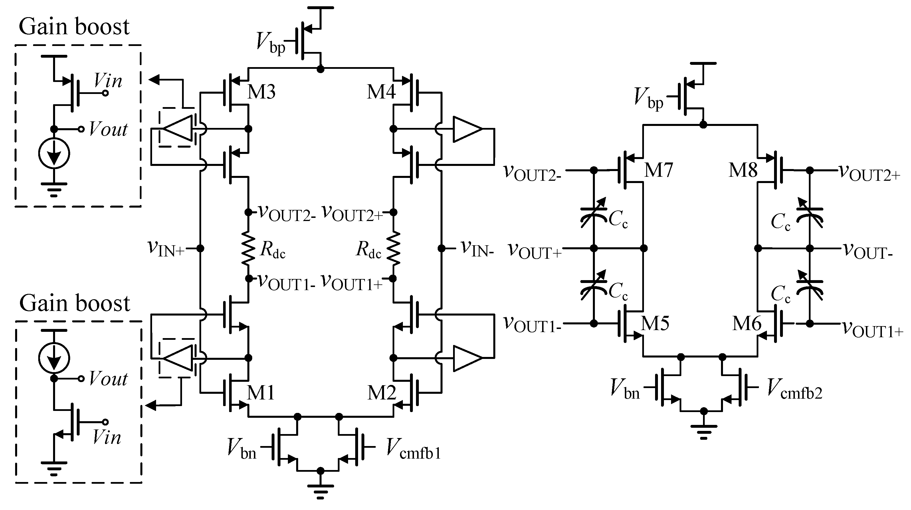
Figure 1a shows a conventional two-stage Miller OPAMP with a complementary input structure, where the Common Mode Feedback (CMFB) circuits are omitted for a succinct purpose.
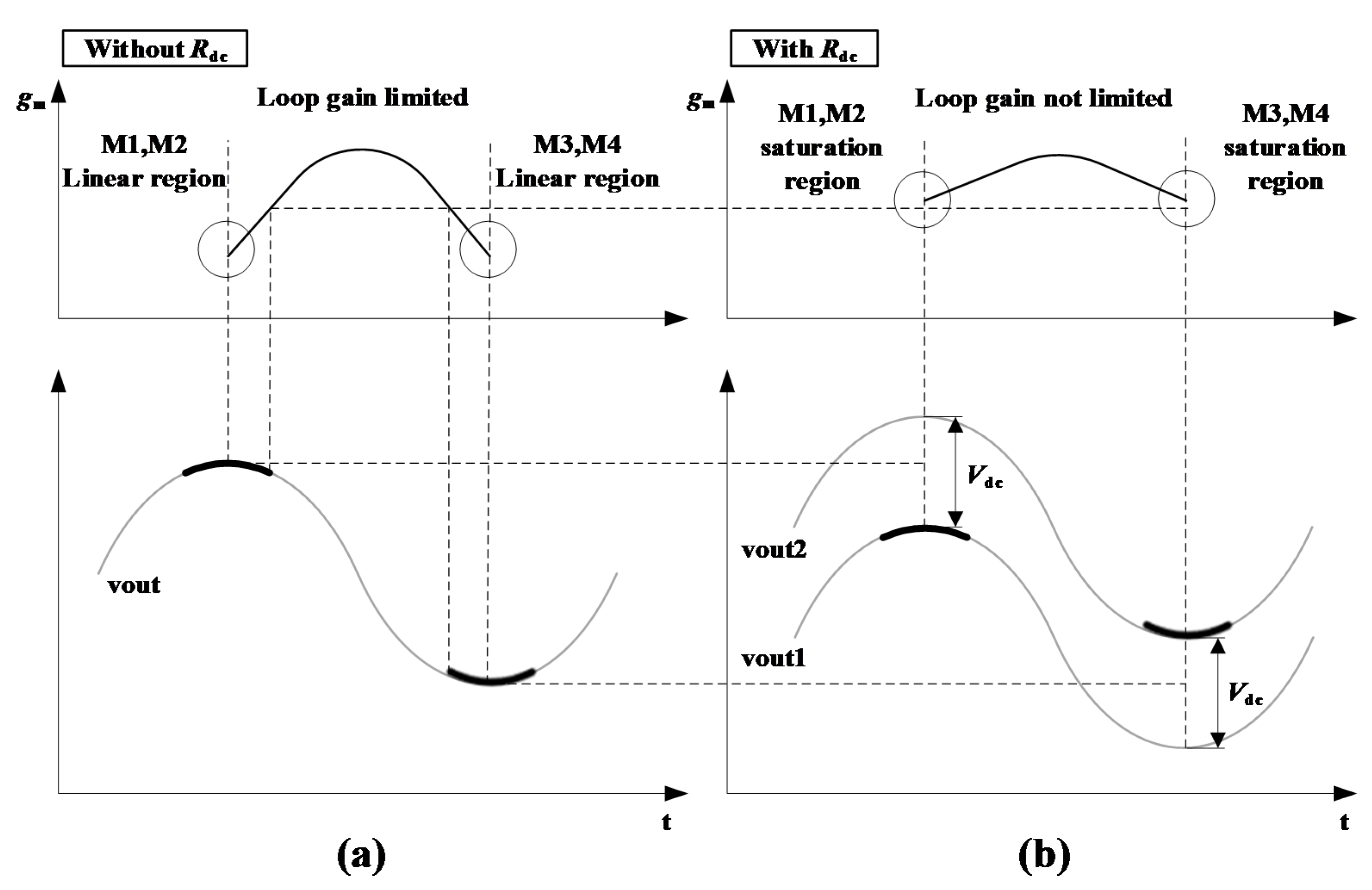
The complementary input topology can realize a higher voltage gain than the OPAMP with a single transistor at the cost of the same current due to the current reuse in the push-pull principle [4]. However, the output swing of the first stage can be very large, owing to the high voltage gain of the LPF. Although the output terminal of the first stage can be biased at an adequate DC voltage to guarantee all the transistors in the second stage not entering the cutoff region, the large output swing can make half of the transistors in the second stage enter the linear region, which still seriously limits the voltage gain of the OPAMP. As is shown in Figure 2a, NMOS transistors M1 and M2 enter the linear region when the output voltage swings to the maximum point, while PMOS transistors M3 and M4 enter the linear region when the output voltage swings to the minimum point. Therefore, the voltage gain is limited when the input terminals of M1–M4 are biased at the same DC voltage.
Figure 1b shows the OPAMP topology with the transconductance equalization technique proposed in this paper. With a pair of resistors R d c , NMOS and PMOS transistors are biased at different DC voltages to avoid M1–M4 entering the linear region. As shown in Figure 2b, with the V d c generated by the R d c , NMOS transistors M1 and M2 are biased at a lower DC voltage to be prevented from entering the linear region when the output signal swings to the maximum point, while PMOS transistors M3 and M4 are biased at a higher DC voltage to be prevented from entering the linear region when the output signal swings to the minimum point. Although the voltage gain can still be limited by the channel length modulation under a large input swing, all transistors of the second stage operating in the saturation region can alleviate transconductance limitation effectively.

2.2. DCOC Method

The IM2 of the DCR is mainly introduced by mismatches between the N path and P path of the mixer, TIA, and LPF, which are mainly introduced by DC offsets from the input terminals of the mixer, TIA, and LPF. Consequently, the IM2 can be depressed by reducing the DC offset [23,24]. More precisely, the output signal of the N and P terminals y p ( t )   and   y n ( t ) responds to an input signal x ( t ) as shown by Equation (1). Note that we only consider the second-order distortion:
y p ( t ) = α 1 p x ( t ) + α 2 p x ( t ) 2 y n ( t ) = α 1 n x ( t ) + α 2 n x ( t ) 2 y p ( t ) y n ( t ) = ( α 1 p α 1 n ) x ( t ) + ( α 2 p α 2 n ) x ( t ) 2
where α 1 p   and   α 1 n are the responses of the first order and the second order, respectively. From the third equation in Equation (1), we can see that ( α 2 p α 2 n ) x ( t ) 2 is introduced as the second-order distortion by mismatches between the N and P paths due to the DC offsets. Therefore, a hybrid DCOC method is proposed to depress mismatches of the TIA and the LPF in Figure 3 to depress the IM2.
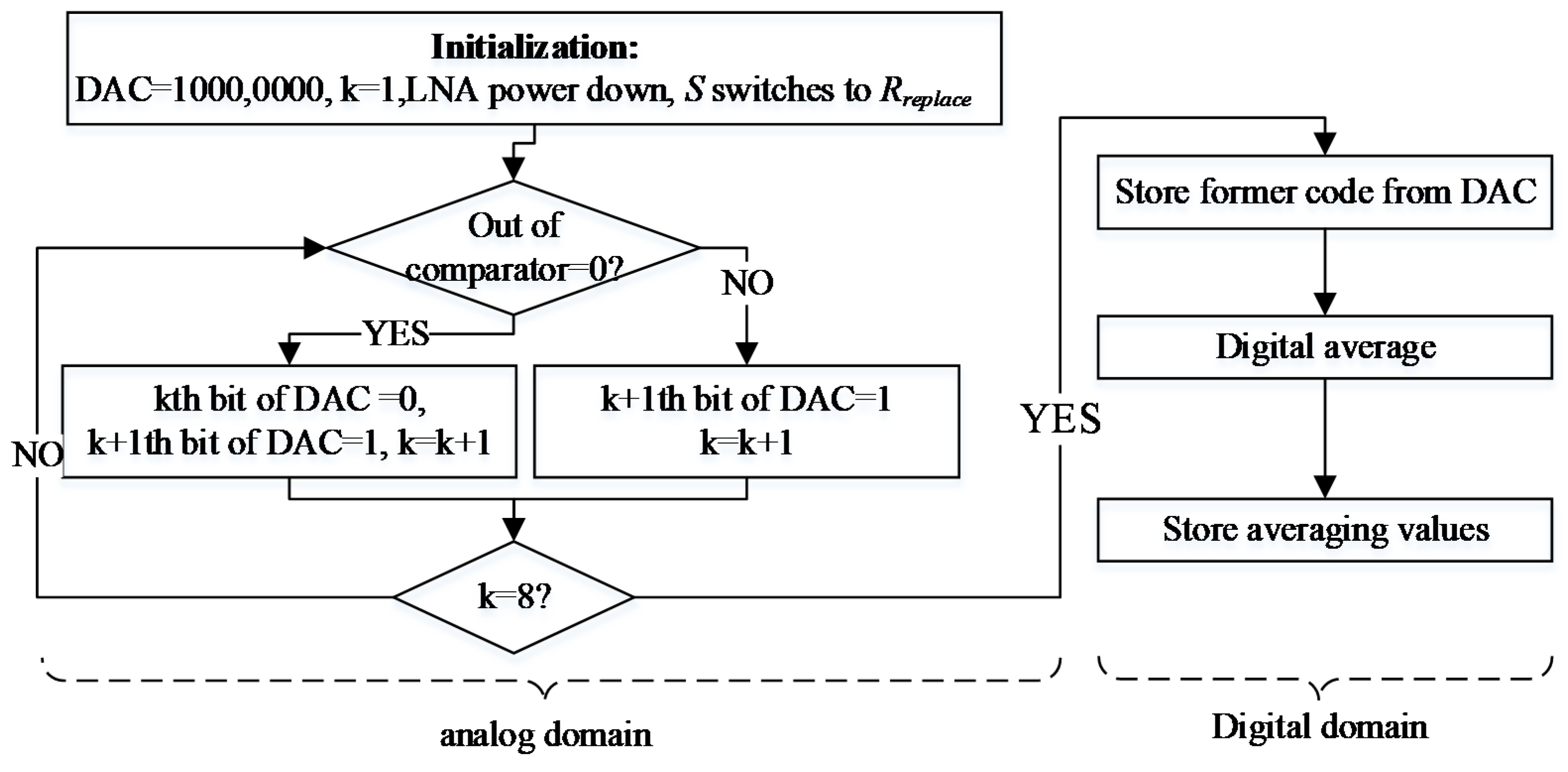
The proposed DC offset calibration method is shown in Figure 4. The initial value of the DAC is set to 10,000,000 at the beginning so that the DAC offers almost the same current (only 1 LSB of difference) to the differential ends of the mixer and the LPF circuits. To ensure that the signal received by the antenna has not interfered during the DC calibration process, the LNA should be powered down by connecting to R r e p l a c e , the equivalent resistance of the LNA. With the mixer path connected to R r e p l a c e , the transfer function of the DC offset is stabilized during calibration to validate the calibration results. During the process of calibration, the DAC is controlled by a successive approximation algorithm (SAR) to compensate for the DC offset. Finally, the DAC output is averaged by a digital averaging circuit to obtain the remaining DC offset, which is restored in registers together with the previous calibration results of the DAC.

3. Circuit Designs

The architecture of the DCR with proposed high-linearity methods in this paper is shown in Figure 3, including the broadband low-noise amplifiers, mixers, low-pass filters, analog-to-digital converters (ADC), and DC offset calibration circuits.
Among them, the DC offset calibration circuit includes two programmable resistors used to replace the output impedance of the low-noise amplifier during the calibration process, four DACs, and four comparators for the compensation and detection of the DC offset, respectively, in the analog domain. Two digital averaging circuits are employed for detecting the residual DC offset and DC offset calibration control algorithm.

3.1. RC-Active LPF Based on a Complementary OPAMP with the Proposed Transconductance Equalization Technique

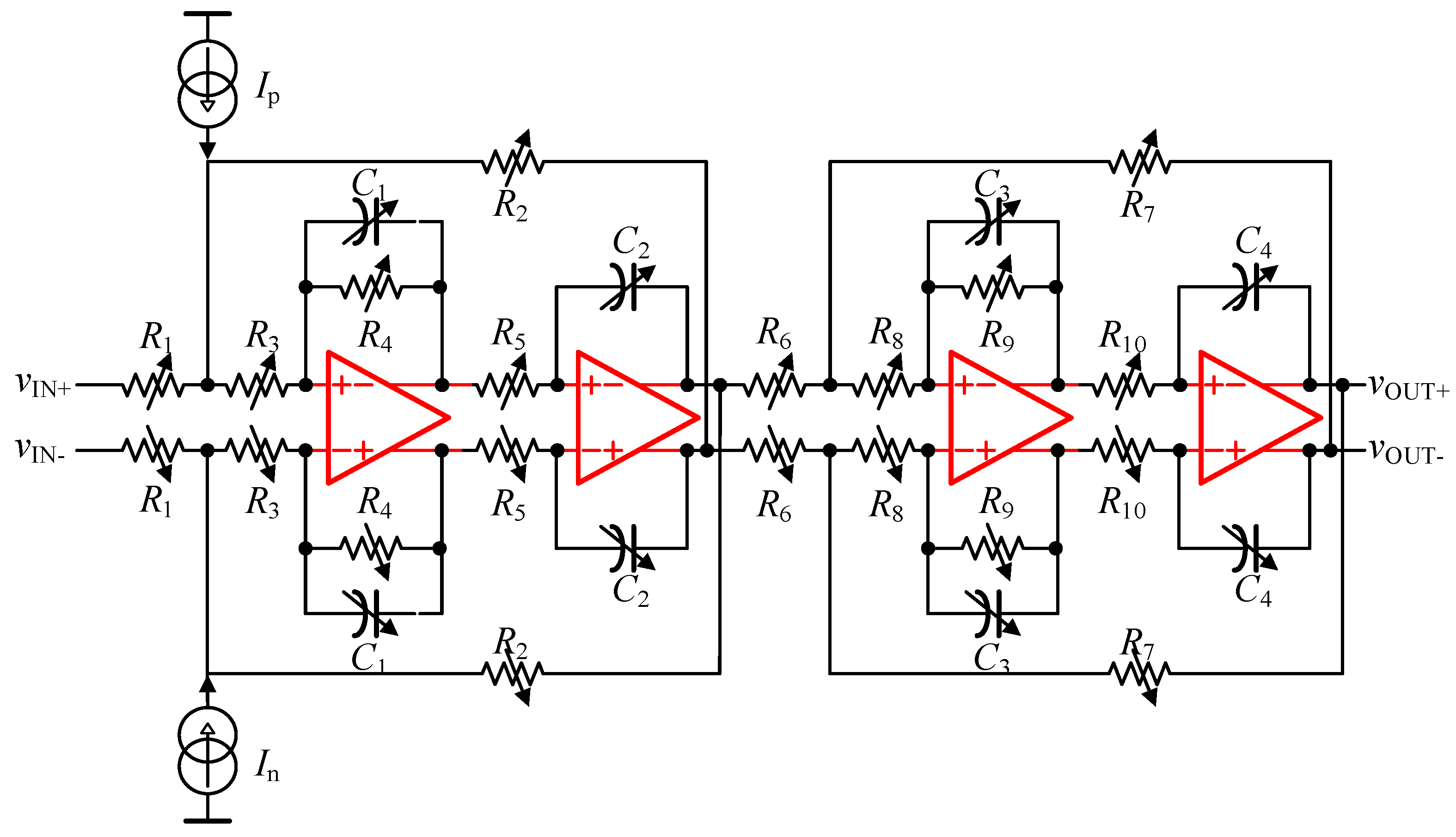
The proposed DCR adopted a two-stage Tow-Thomas biquad structure to implement a four-stage Chebyshev low-pass filter. The circuit block diagram is shown in Figure 5. By configuring the resistance and capacitance value, a gain range of 0–23 dB and a bandwidth range of 1–32 MHz could be achieved, and together with the previous transconductance amplifier in the mixer, a gain range of 5–65 dB could be achieved. The parameters of the transconductance amplifier of the mixer and the LPF are shown in Table 1.
The linearity of the LPF was determined by the overdrive voltage of the input transistors of the OPAMP and the loop gain of each stage of the LPF, so the OPAMP must have had a sufficiently high DC gain and gain bandwidth (GBW) [25,26]. The OPAMP adopted a two-stage Miller topology, and the circuit diagram is shown in Figure 6.
In order to improve the linearity, both stages of the OPAMP adopted the topology of the N and P complementary inputs to realize complementary transconductance. By employing the transconductance equalization technique, the gate terminals of the second-stage NMOS transistors M5 and M6 and PMOS transistors M7 and M8 were biased at different DC voltages so as to avoid large swing signals at the output terminal of the first stage, resulting in M5–M8 operating in the linear region. In addition, the operational amplifier employed cascade and gain boost technology to achieve an extremely high DC gain. The R d c was 638 ohms, while the Miller capacitor C c was configurable to adjust the gain bandwidth of the OPAMP to meet the requirements of different IF bandwidths.
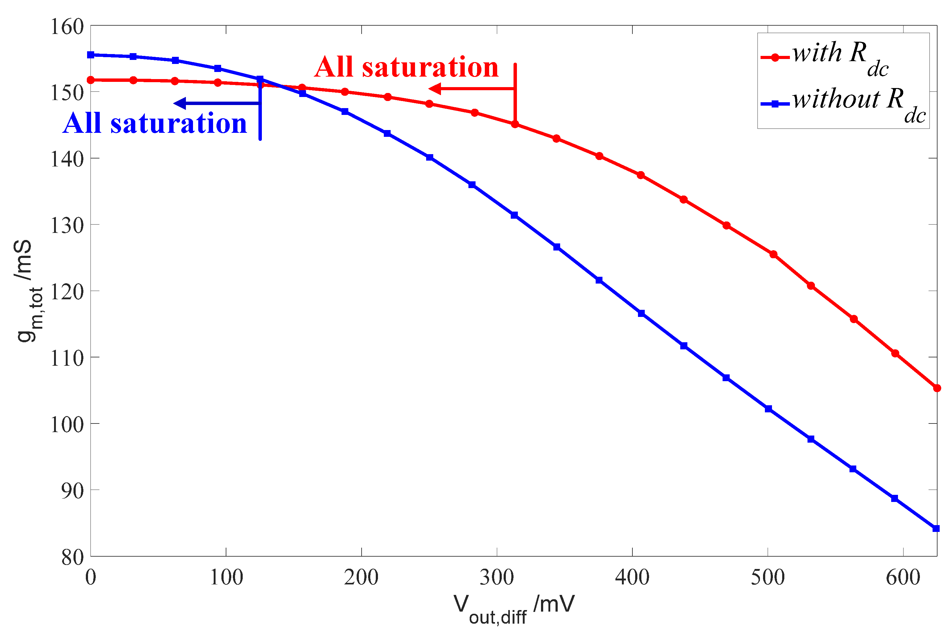
To confirm this, the total transconductance g m , t o t a l of the input transistors of the second stage of the OPAMPs with and without R d c as the differential output voltage of the LPF was swept from 0 to 625 mV (1.3 V p p , maximum output power 6 dBm) is plotted in Figure 7. To confirm that the simulation results were valid for all IF frequencies, voltage gains, and all OPAMPs in the LPF, the voltage gain and bandwidth of the LPF were set to 23 dB and 32 MHz, respectively, while the g m , t o t a l of the last-stage OPAMP of the LPF, operated in the largest input and output voltage swing, was adopted in the simulation.
From Figure 7, we can see that the transconductance of the second stage of the OPAMP with R d c was less suppressed than that of the OPAMP without R d c under an increasing voltage swing than that without R d c . Furthermore, the DC simulation results show that all the input transistors operated in the saturation region in the OPAMP with R d c when the differential output swing was less than 313.3 mV (627 m V p p , output power 0 dBm), while those operating in the saturation region in the OPAMP without R d c when the differential output swing was less than 125.1 mV. Although the maximum g m , t o t a l of the OPAMP without R d c was a little bit larger than that with R d c , attributed to the channel length modulation effect, the linearity of the LPF could be improved by R d c for a more stable voltage gain of the OPAMP, especially under a large output swing. To valid this, simulation of OIP3 for two closely spaced tones (1 MHz) with a total output amplitude of 632 m V p p (total output power 0 dBm) as their frequency was swept from 0.25 f o to 1.75 f o ( f o   = 16 MHz) is plotted in Figure 8. To confirm that the results could be adopted in all IF frequencies and voltage gains, the bandwidth and voltage gain of the LPF were set to 32 MHz and 23 dB, respectively.
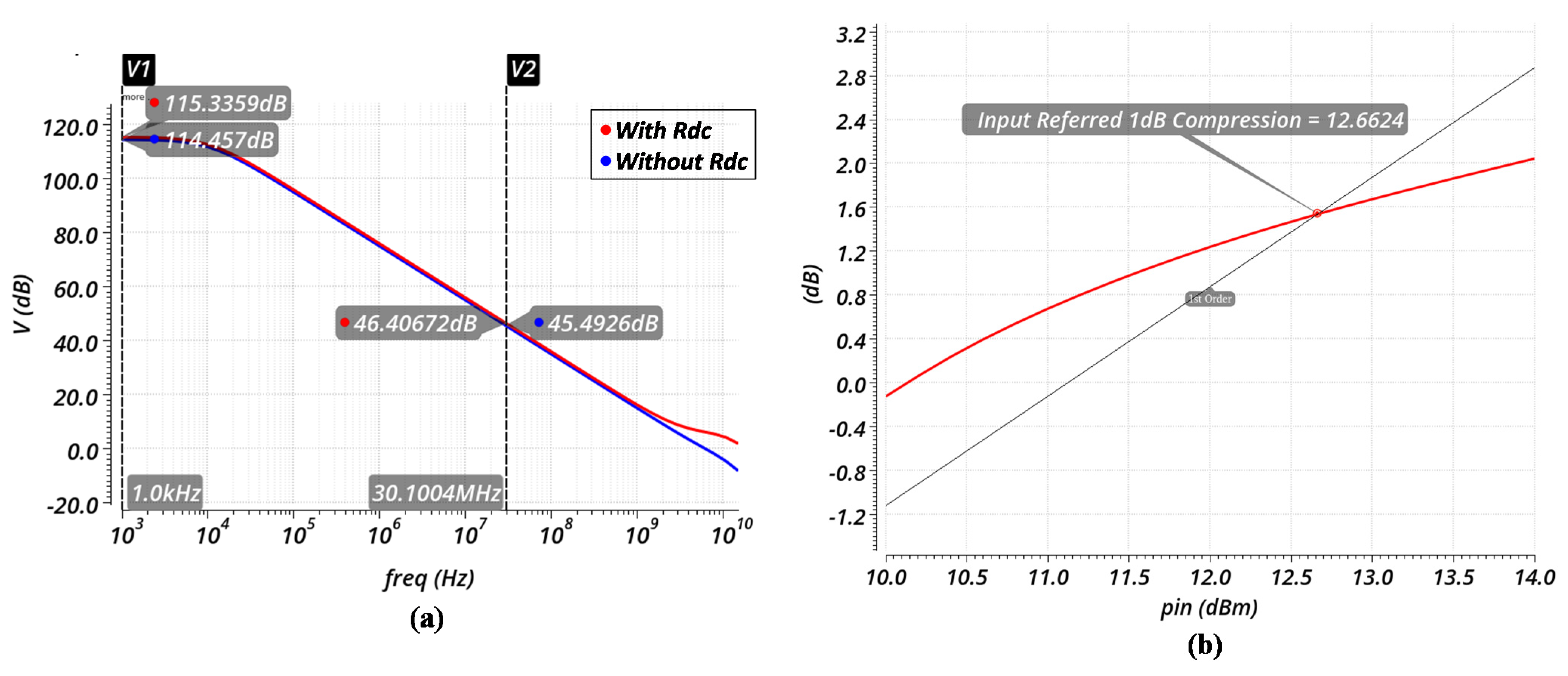
From Figure 8, we can see that the OIP3 of the LPF was improved by approximately 7 dB under an output swing of 632 m V p p in all IF frequencies, while the LPF could realize a maximum OIP3 of 40.7 dBm with a voltage gain of 23 dB. The simulation results of the frequency response of the gain with and without R d c of the proposed Opamp and the 1-dB compression point of the LPF with the proposed OPAMP are shown in Figure 9a,b, respectively. Note that the 1-dB compression point was simulated with a gain of 0 dB.

3.2. DCOC Circuits

To calibrate the DC offset effectively and prevent the DC offset from the RF front end being amplified by the LPF, the calibration was operated at the output terminal of the RF front end and the LPF. The DC offset of the RF front end was mainly introduced by the circuit mismatch in the signal path, while the DC offset of the LPF was mainly caused by the circuit mismatches and that of the RF front end. It was assumed that the equivalent DC offset of the mixer at the input terminal of the OPAMP of the TIA was V o s i n , as shown in Figure 10.
Consequently, the DC offset of the mixer could be given by
V o s o u t , m i x = ( 1 + R f R o u t I F ) V o s i n + ( I n I p ) R f
where R o u t I F is the equivalent output resistance of the mixer and R f is the feedback resistor of the TIA. Since the passive mixer could transform the impedance at both ends of itself at the frequencies, the equivalent output resistance R o u t I F of the passive mixer was proportional to the output impedance of the transconductance stage [27,28,29]. Therefore, Z o u t R F could be expressed as follows:
Z o u t R F = ( 1 2 π f L O C 1 _ p a r a + R o u t ) ( 1 + 2 π f L O C 1 _ p a r a R o u t 2 π f L O C 1 _ p a r a R o u t 1 G m ) ( 1 2 π f L O C 2 _ p a r a )
where R o u t is the output impedance of the LNA, C 1 _ p a r a and C 2 _ p a r a are the parasitic capacitances that are less than 80 fF according to the simulation, and G m is the transconductance of the mixer. With R o u t being different under different gains of the LNA and the increasing f L O , the equivalent output resistance of the mixer would drop dramatically [30]. Therefore, to confirm the accuracy of the DC offset calibration, R o u t should be replaced by R r e p l a c e with a constant resistance, as shown in Figure 10. Moreover, the DC offset needed to be recalibrated for different local oscillator frequencies and gains [31].
On the other hand, the DC offset of the LPF mainly came from that of the mixer and the circuit mismatches. It was assumed that V o s i n 1 and V o s i n 2 were the equivalent input DC offset voltages of the first and second stage of the low-pass filter, respectively. The output DC offset could be expressed as
V o s o u t , L P F = R 2 R 1 R 7 R 6 V o s o u t , m i x ( 1 + R 2 R 1 ) R 7 R 6 V o s i n 1 + ( 1 + R 7 R 6 ) V o s i n 2 ( I n I p ) R 2 R 7 R 6
where R 2 / R 1 and R 7 / R 6 are the voltage gain of the first stage and second stage of the LPF, respectively. It can be seen from Equation (4) that for different gains and IF bandwidths, the DC offset should be recalibrated.
According to the previous calculation, the parameters of the DAC could be confirmed. The calibration accuracy and range of the DC offset depended on the circuit parameters of the DAC [32]. Therefore, the least significant bit (LSB) of the DAC should be less than the minimum DC offset of the mixers and LPF, while the total current of the DAC should be larger than the maximum DC offset of the mixers and the LPF [30]. According to the equivalent input DC offset voltage of the OPAMP through Monte Carlo simulation [33] and the gain of the mixers and LPF shown in Table 1, the DAC employed in the DCOC circuits is shown in Figure 11. This was an 8-bit, full-thermometer, current-steering DAC with an LSB current of 120 nA, which could ensure that the output DC offset of the mixer and low-pass filter could be limited to less than −50 dBFS (differential of 1.4 mV, ADC full swing of 6.5 dBm) after calibration in the analog domain.

4. Measurement Results

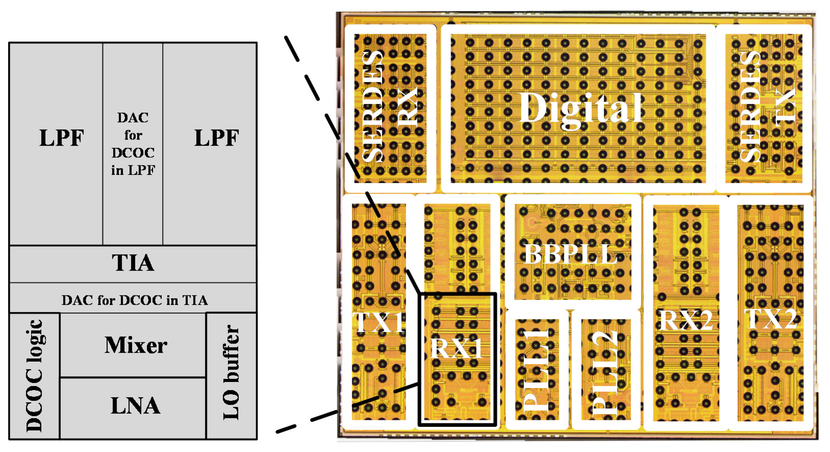
Based on the RF transceiver system with two receivers and two transmitters, the DCR was fabricated in 40-nm CMOS technology. The chip photo of the receiver is shown in Figure 12. The chip area of the whole receiver (excluding ADC) was 1.15 mm2, and it consumed 126 mA of current under a voltage supply of 1.3 V.
Figure 13a shows the S11 result of the receiver. It can be seen that this DCR could achieve −10 dB input matching in the full frequency band. Through the frequency spectrum analysis of the ADC output signal, it can be seen in Figure 13b that the receiver could achieve a noise figure of 3.5 dB at a frequency offset of 3 MHz in the full frequency band.
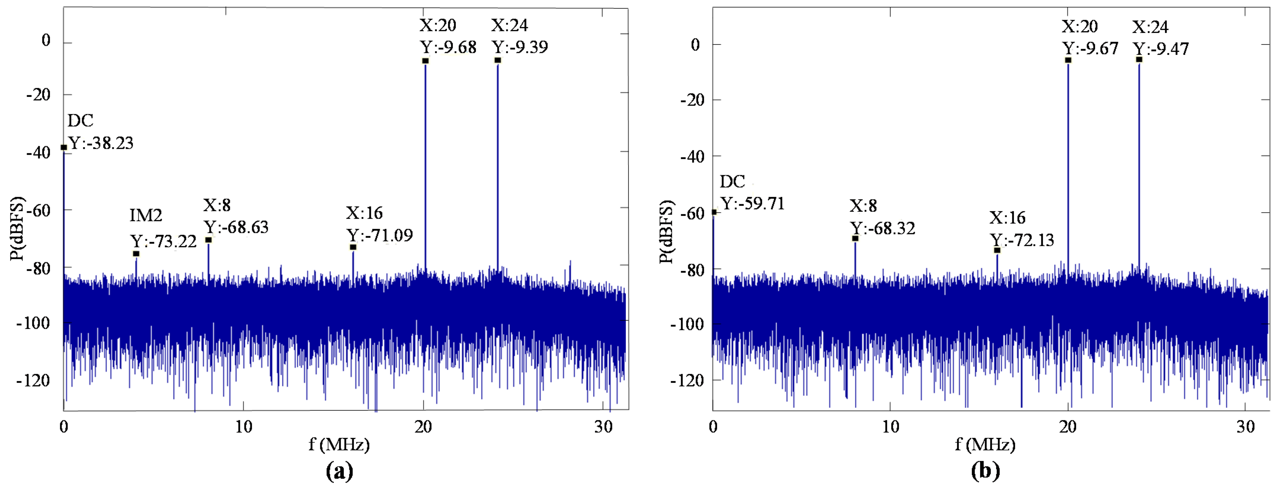
In order to measure the linearity of the receiver under the maximum IF bandwidth, the receiver gain was configured to 60 dB (low noise amplifier: 15 dB; mixer: 27 dB; and filter: 18 + 0 dB), while the full swing of the ADC was 6.5 dBm. Figure 14a,b shows the linearity test results of the receiver at an RF frequency of 2.5 GHz before and after DC offset calibration. It can be seen that the receiver could achieve an OIP3 of 28 dBm. After DC offset calibration, the IM2 was improved by more than 10 dBc to more than 70 dBc, and the remaining DC was reduced by 21 dBm to −53.2 dBm.
Table 2 is the performance comparison between the proposed DCR and other references in recent years. It can be seen that this DCR could achieve a better noise figure and higher linearity of better suppression for both IM2 and IM3 in a wideband range.

5. Conclusions

This paper presents two high-linearity methods for a DCR to realize better IP2 and IP3 values. In order to improve IP3, a complementary input operational amplifier in the LPF was adopted in the DCR. To improve IP2, a digital-analog hybrid DC offset calibration method was proposed based on the structure of the mixer and LPF. After being fabricated in 40-nm CMOS technology, the measurement results show that the DCR could achieve a noise figure of 2.6–3.5 dB in the full frequency band, an IIP3 of 10 dB, an OIP3 of 28 dBm, an IM2 of more than 70 dBc, and a remaining DC offset of −53.2 dBm under a total voltage gain of 60 dB.

Author Contributions

Methodology, Y.H.; data curation, F.W.; writing—original draft preparation, Y.H.; writing—review and editing, Z.W.; project administration and funding acquisition, J.L.; supervision, F.Y. All authors have read and agreed to the published version of the manuscript.

Funding

This research received no external funding.

Acknowledgments

The authors would like to thank the Institute of Aerospace Electronics Engineering of Zhejiang University for providing a research platform and technical support.

Conflicts of Interest

The authors declare no conflict of interest.

References

  1. Razavi, B. Design considerations for direct-conversion receivers. IEEE Trans. Circuits Syst. II Analog Digit. Signal Process. 1997, 44, 428–435. [Google Scholar] [CrossRef] [Green Version]
  2. Lim, J.; Kim, J. A 20-kHz~16-MHz Programmable-Bandwidth 4th Order Active Filter Using Gain-Boosted Opamp With Negative Resistance in 65-nm CMOS. IEEE Trans. Circuits Syst. II Express Briefs 2018, 66, 182–186. [Google Scholar] [CrossRef]
  3. Thyagarajan, S.V.; Pavan, S.; Sankar, P. Active-RC filters using the Gm-assisted OTA-RC technique. IEEE J. Solid State Circuits 2011, 46, 1522–1533. [Google Scholar] [CrossRef]
  4. Ye, L.; Shi, C.; Liao, H.; Huang, R.; Wang, Y. Highly power-efficient active-RC filters with wide bandwidth-range using low-gain push-pull opamps. IEEE Trans. Circuits Syst. I Regul. Pap. 2012, 60, 95–107. [Google Scholar] [CrossRef]
  5. Kousai, S.; Hamada, M.; Ito, R.; Itakura, T. A 19.7 MHz, fifth-order active-RC Chebyshev LPF for draft IEEE802. 11n with automatic quality-factor tuning scheme. IEEE J. Solid State Circuits 2007, 42, 2326–2337. [Google Scholar] [CrossRef]
  6. Harrison, J.; Weste, N. A 500 MHz CMOS anti-alias filter using feed-forward op-amps with local common-mode feedback. In Proceedings of the 2003 IEEE International Solid-State Circuits Conference, Digest of Technical Papers, ISSCC 2003, San Francisco, CA, USA, 13 February 2003; pp. 132–483. [Google Scholar]
  7. Laxminidhi, T.; Prasadu, V.; Pavan, S. Widely programmable high-frequency active RC filters in CMOS technology. IEEE Trans. Circuits Syst. I Regul. Pap. 2008, 56, 327–336. [Google Scholar] [CrossRef]
  8. Wu, W.; Mo, T.; Lu, Z. A 180 nm CMOS three stage feedforward compensation op-amp with linearity improvement technique for active RC LPF. In Proceedings of the 2016 10th IEEE International Conference on Anti-counterfeiting, Security, and Identification (ASID), Xiamen, China, 23–25 September 2016; pp. 91–95. [Google Scholar]
  9. Fary, F.; Mangiagalli, L.; Vallicelli, E.; De Matteis, M.; Baschirotto, A. A 28 nm bulk-CMOS 50MHz 18 dBm-IIP3 Active-RC Analog Filter based on 7 GHz UGB OTA. In Proceedings of the ESSCIRC 2019—IEEE 45th European Solid State Circuits Conference (ESSCIRC), Cracow, Poland, 23–26 September 2019; pp. 253–256. [Google Scholar]
  10. Ballo, A.; Grasso, A.D.; Pennisi, S. Active load with cross-coupled bulk for high-gain high-CMRR nanometer CMOS differential stages. Int. J. Circuit Theory Appl. 2019, 47, 1700–1704. [Google Scholar] [CrossRef]
  11. Ballo, A.; Grasso, A.D.; Pennisi, S.; Venezia, C. High-Frequency Low-Current Second-Order Bandpass Active Filter Topology and Its Design in 28-nm FD-SOI CMOS. J. Low Power Electron. Appl. 2020, 10, 27. [Google Scholar] [CrossRef]
  12. Cao, M.; Zheng, Y.; Garg, H. A novel algorithm for DC offsets and flicker noise cancellation in direct conversion receivers. In Proceedings of the 2004 Ninth International Conference onCommunications Systems, ICCS 2004, Singapore, 7 September 2004; pp. 441–445. [Google Scholar]
  13. Namgoong, W. DC-offset and 1/f noise effects on AC-coupled direct-conversion receiver. In Proceedings of the 44th IEEE 2001 Midwest Symposium on Circuits and Systems. MWSCAS 2001 (Cat. No. 01CH37257), Dayton, OH, USA, 14–17 August 2001; pp. 886–889. [Google Scholar]
  14. Kuo, M.-C.; Kao, S.-W.; Chen, C.-H.; Hung, T.-S.; Shih, Y.-S.; Yang, T.-Y.; Kuo, C.-N. A 1.2 V 114 mW Dual-Band Direct-Conversion DVB-H Tuner in 0.13 μm CMOS. IEEE J. Solid State Circuits 2009, 44, 740–750. [Google Scholar] [CrossRef]
  15. Chu, X.; Lin, M.; Gong, Z.; Shi, Y.; Dai, F.F. A CMOS programmable gain amplifier with a novel DC-offset cancellation technique. In Proceedings of the IEEE Custom Integrated Circuits Conference 2010, San Jose, CA, USA, 19–22 September 2010; pp. 1–4. [Google Scholar]
  16. Ye, L.; Liao, H.; Song, F.; Chen, J.; Li, C.; Zhao, J.; Liu, R.; Wang, C.; Shi, C.; Liu, J. A single-chip CMOS UHF RFID reader transceiver for Chinese mobile applications. IEEE J. Solid State Circuits 2010, 45, 1316–1329. [Google Scholar] [CrossRef]
  17. Moezzi, M.; Mousavi, S.F.; Ashtari, P. An area-efficient DC offset cancellation architecture for zero-IF DVB-H receivers. IEEE Microw. Wirel. Compon. Lett. 2018, 28, 813–815. [Google Scholar] [CrossRef]
  18. Harpe, P.; Zhou, C.; Philips, K.; de Groot, H. A 1.6 mW 0.5 GHz open-loop VGA with fast startup and offset calibration for UWB radios. In Proceedings of the 2011 Proceedings of the ESSCIRC (ESSCIRC), Helsinki, Finland, 12–16 September 2011; pp. 103–106. [Google Scholar]
  19. Oh, S.-M.; Park, K.-S.; Yoo, H.-H.; Na, Y.-S.; Kim, T.-S. A design of DC offset canceller using parallel compensation. In Proceedings of the 2007 IEEE International Symposium on Circuits and Systems, New Orleans, LA, USA, 27–30 May 2007; pp. 1685–1688. [Google Scholar]
  20. Yoshida, H.; Tsurumi, H.; Suzuki, Y. DC offset canceller in a direct conversion receiver for QPSK signal reception. In Proceedings of the Ninth IEEE International Symposium on Personal, Indoor and Mobile Radio Communications (Cat. No. 98TH8361), Boston, MA, USA, 8–11 September 1998; pp. 1314–1318. [Google Scholar]
  21. Zheng, F.; Guo, Q.; Liu, J.; Tan, X.; Min, H. A new DC cancellation technique for a mixer-first receiver in UHF RFID reader. In Proceedings of the 2016 13th IEEE International Conference on Solid-State and Integrated Circuit Technology (ICSICT), Hangzhou, China, 25–28 October 2016; pp. 1564–1566. [Google Scholar]
  22. Liu, J.; Guo, Q.; Wang, Y.; Tan, X.; Min, H. An area-efficient digitally-assisted DC canceling loop for high sensitivity UHF RFID receiver. In Proceedings of the 2016 IEEE International Conference on RFID Technology and Applications (RFID-TA), Foshan, China, 21–23 September 2016; pp. 166–171. [Google Scholar]
  23. Fang, S.J.; Lee, S.T.; Allstot, D.J.; Bellaouar, A. A 2 GHz CMOS even harmonic mixer for direct conversion receivers. In Proceedings of the 2002 IEEE International Symposium on Circuits and Systems (Cat. No. 02CH37353), Phoenix-Scottsdale, AZ, USA, 26–29 May 2002; p. IV. [Google Scholar]
  24. Huang, Y.; Li, W.; Hu, S.; Xie, R.; Li, X.; Fu, J.; Sun, Y.; Pan, Y.; Chen, H.; Jiang, C. A High-Linearity WCDMA/GSM Reconfigurable Transceiver in 0.13-μm CMOS. IEEE Trans. Microw. Theory Tech. 2012, 61, 204–217. [Google Scholar] [CrossRef]
  25. Crols, J.; Steyaert, M.S. A 1.5 GHz highly linear CMOS downconversion mixer. IEEE J. Solid State Circuits 1995, 30, 736–742. [Google Scholar] [CrossRef]
  26. Xie, R.; Jiang, C.; Li, W.; Huang, Y.; Hong, Z. A dual-mode analog baseband utilizing digital-assisted calibration for WCDMA/GSM receivers. In Proceedings of the 2011 9th IEEE International Conference on ASIC, Xiamen, China, 25–28 October 2011; pp. 1058–1061. [Google Scholar]
  27. Valla, M.; Montagna, G.; Castello, R.; Tonietto, R.; Bietti, I. A 72-mW CMOS 802.11 a direct conversion front-end with 3.5-dB NF and 200-kHz 1/f noise corner. IEEE J. Solid State Circuits 2005, 40, 970–977. [Google Scholar] [CrossRef]
  28. Redman-White, W.; Leenaerts, D. 1/f noise in passive CMOS mixers for low and zero IF integrated receivers. In Proceedings of the 27th European Solid-State Circuits Conference, Villach, Austria, 18–20 September 2001; pp. 41–44. [Google Scholar]
  29. Sacchi, E.; Bietti, I.; Erba, S.; Tee, L.; Vilmercati, P.; Castello, R. A 15 mW, 70 kHz 1/f corner direct conversion CMOS receiver. In Proceedings of the IEEE 2003 Custom Integrated Circuits Conference, San Jose, CA, USA, 24 September 2003; pp. 459–462. [Google Scholar]
  30. Wang, F.; Fan, L.; Shen, Y.; Chen, H.; Liu, J.; Wang, Z.; Yu, F. An effective DC offset calibration method combined with analog and digital circuits for direct conversion receivers. IEICE Electron. Express 2019, 16, 20190518. [Google Scholar] [CrossRef] [Green Version]
  31. Vassiliou, I.; Vavelidis, K.; Georgantas, T.; Plevridis, S.; Haralabidis, N.; Kamoulakos, G.; Kapnistis, C.; Kavadias, S.; Kokolakis, Y.; Merakos, P. A single-chip digitally calibrated 5.15–5.825-GHz 0.18-μm CMOS transceiver for 802.11 a wireless LAN. IEEE J. Solid State Circuits 2003, 38, 2221–2231. [Google Scholar] [CrossRef]
  32. Shih, H.-Y.; Kuo, C.-N.; Chen, W.-H.; Yang, T.-Y.; Juang, K.-C. A 250 MHz 14 dB-NF 73 dB-gain 82 dB-DR analog baseband chain with digital-assisted DC-offset calibration for ultra-wideband. IEEE J. Solid State Circuits 2010, 45, 338–350. [Google Scholar] [CrossRef]
  33. Bakar, F.A.; Murad, S.A.Z.; Ismail, R.C.; Saari, V.; Halonen, K. A 9-bit current-steering Digital to Analog Converter for differential dc-offset compensation of a baseband chain. In Proceedings of the 2014 IEEE Student Conference on Research and Development, Penang, Malaysia, 16–17 December 2014; pp. 1–4. [Google Scholar]
  34. Chang, S.; Shin, H. 2.4-GHz CMOS Bluetooth RF Receiver With Improved IM2 Distortion Tolerance. IEEE Trans. Microw. Theory Tech. 2020, 68, 4589–4598. [Google Scholar] [CrossRef]
  35. Wu, W.; Zhang, L.; Wang, Y. A PVT-robust analog baseband with DC offset cancellation for FMCW automotive radar. IEEE Access 2019, 7, 43249–43257. [Google Scholar] [CrossRef]
  36. Alaei, M.A.; Golabighezelahmad, S.; de Boer, P.-T.; van Vliet, F.E.; Klumperink, E.A.; Kokkeler, A.B. Interference Mitigation by Adaptive Analog Spatial Filtering for MIMO Receivers. IEEE Trans. Microw. Theory Tech. 2021. [Google Scholar] [CrossRef]
Figure 1. (a) Diagram of conventional two-stage complementary input OPAMP. (b) Diagram of two-stage complementary input OPAMP with proposed transconductance equalization technique.
Electronics 10 01966 g001
Figure 2. (a) Transconductance of the input transistors in the second stage without R d c . (b) Transconductance of the input transistors in the second stage with R d c .
Electronics 10 01966 g002
Figure 3. The block diagram of the direct conversion receiver.
Electronics 10 01966 g003
Figure 4. The flow diagram of the DCOC method.
Electronics 10 01966 g004
Figure 5. The block diagram of the LPF.
Electronics 10 01966 g005
Figure 6. The block diagram of the proposed OPAMP in LPF.
Electronics 10 01966 g006
Figure 7. Simulation results of g m , t o t a l of the second stage of the OPAMPs with and without R d c versus the differential output voltage.
Electronics 10 01966 g007
Figure 8. Simulation results of OIP3 of the LPF with and without R d c versus the IF frequency from 4 to 28 MHz under a total output swing of 632   m V p p (each tone being 316   m V p p ).
Electronics 10 01966 g008
Figure 9. (a) Simulated frequency response of the gain with and without R d c of the proposed OPAMP. (b) Simulated 1-dB compression point of the LPF with the proposed OPAMP. We can see from Figure 9a that the DC gain of the proposed OPAMP could achieve 115 dB, and the R d c had little influence on the frequency response of the OPAMP. Furthermore, the output 1-dB compression point was about 12.6 dBm, which would not influence the linearity of the whole system because the maximum output power of the LPF was less than 6 dBm.
Electronics 10 01966 g009
Figure 10. The block diagram of the RF front end.
Electronics 10 01966 g010
Figure 11. The block diagram of the DAC.
Electronics 10 01966 g011
Figure 12. Chip microphotograph of the receiver.
Electronics 10 01966 g012
Figure 13. (a) Measured S11 results. (b) Measured noise figure results.
Electronics 10 01966 g013
Figure 14. (a) Measured linearity without the DCOC at 2.5 GHz. (b) Measured linearity with the DCOC at 2.5 GHz.
Electronics 10 01966 g014
Table 1. Parameters of the mixer and LPF.
Transconductance Amplifier of the MixerFirst-Stage OPAMP of the LPFSecond-Stage OPAMP of the LPF
Gain R f (Ω)Gain R 1 (Ω)Gain R 6 (Ω)
15–27 dB500–2700
Max BW
0–18 dB100–800
Max BW
0–5 dB340–600
Max BW
400–3200
Min BW
1360–2400
Min BW
Table 2. Measured performance and comparison.
[34][35][36]This Work
Technology65 nm CMOS65 nm CMOS22 nm FD-SOI40 nm CMOS
Supply (V)1.01.20.81.3
RF (MHz)2400N/A700–5700200–2500
IF (MHz)N/A0.07–10N/A1–32
Gain Range (dB)2–6218.2–70.6410–60
IM2 (dBc)31.1N/AN/A>70
OIP3 (dBm)N/A7.82228
DC Remaining (dBm)N/AN/AN/A−53.2
Noise Figure (dB)3.0N/A6.8–9.22.6–3.5
Total Area (mm2)0.75N/A0.521.15
Total Power (mW)3.55N/A19.25–34.75160
Publisher’s Note: MDPI stays neutral with regard to jurisdictional claims in published maps and institutional affiliations.